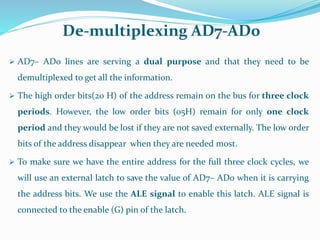
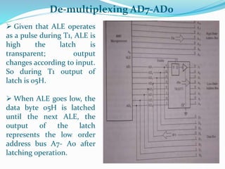
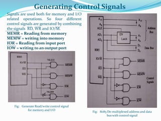
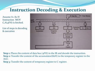
Downloaded 339 times
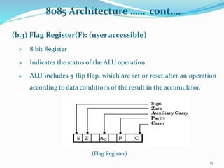
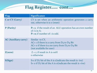
![8085 Architecture …… cont….
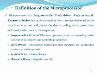
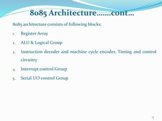
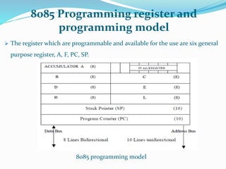
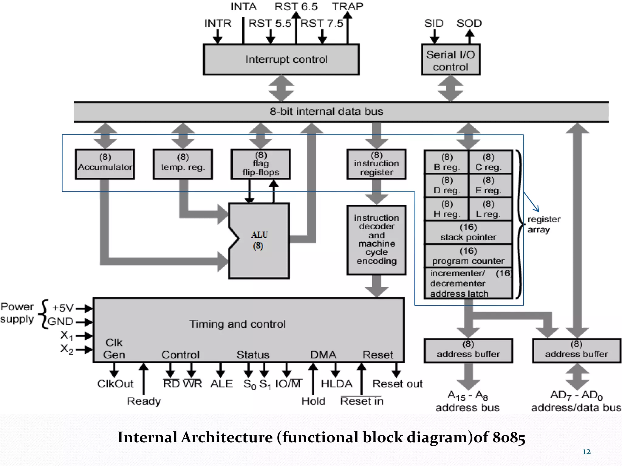
1. Registers Array : 14 register out of which 12 are 8 bit capacity and 2 of 16 bit. Classify into 4 types
(a) General purpose register: (user accessible)
B,C,D,E,H,L are 8 bit register.(can be used singly)
Can also be used for 16-bit register pairs- BC, DE & HL.
Used to store the intermediate data and result
H & L can be used as a data pointer(holds memory address)
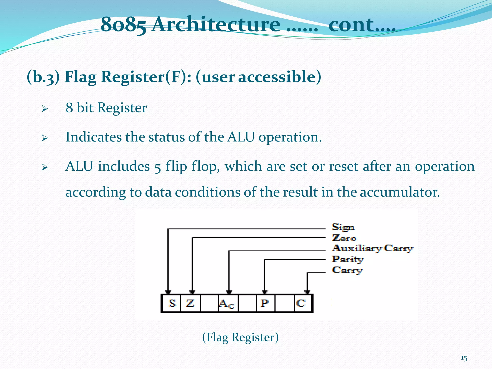
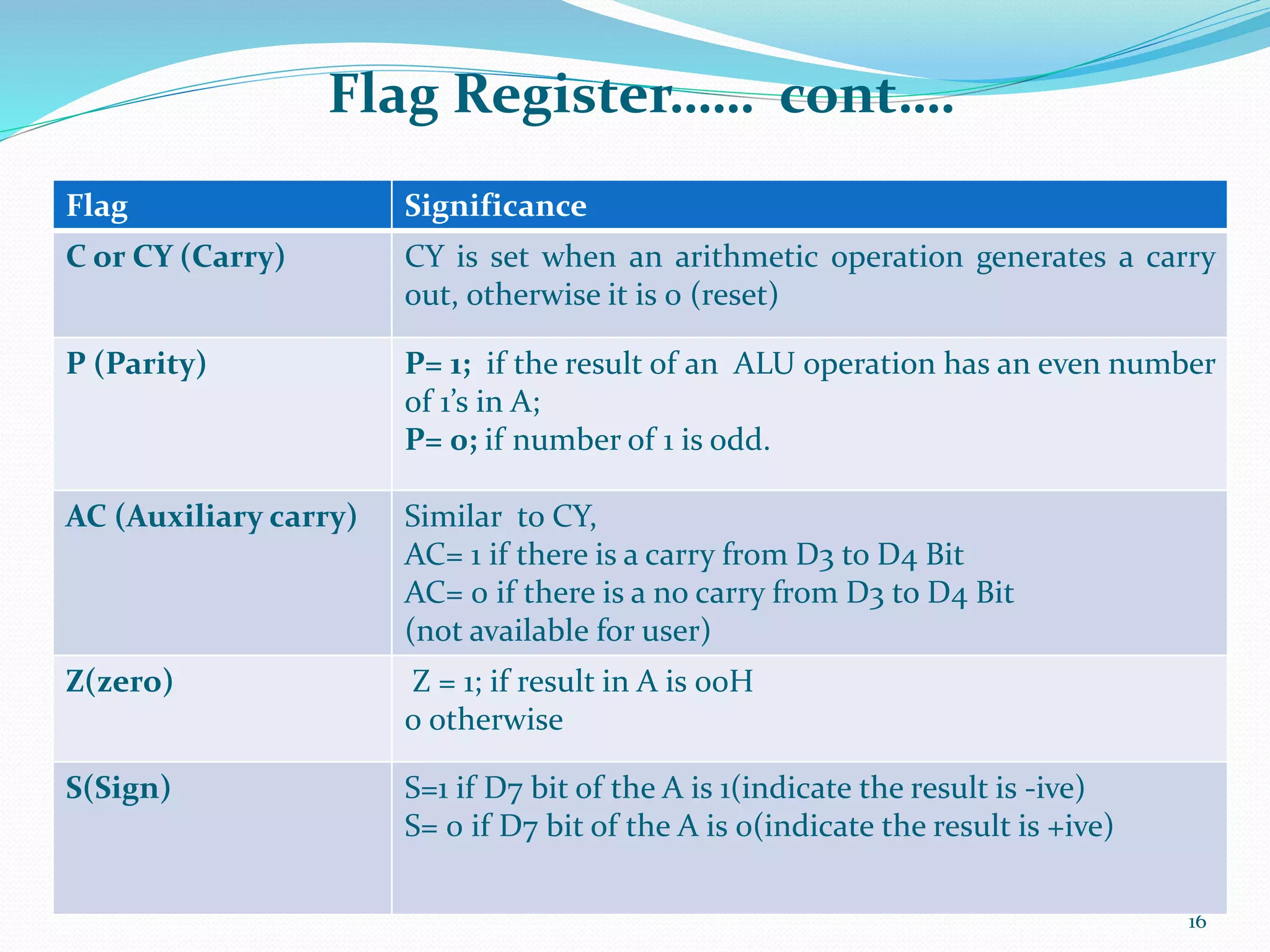
(b) Special Purpose Register[A, Instruction Register and Flag]
(b.1) Accumulator (A): (user accessible)
8 bit register
All the ALU operations are performed with reference to the contents of Accumulator.
Result of an operation is stored in A.
Store 8 bit data during I/O transfer
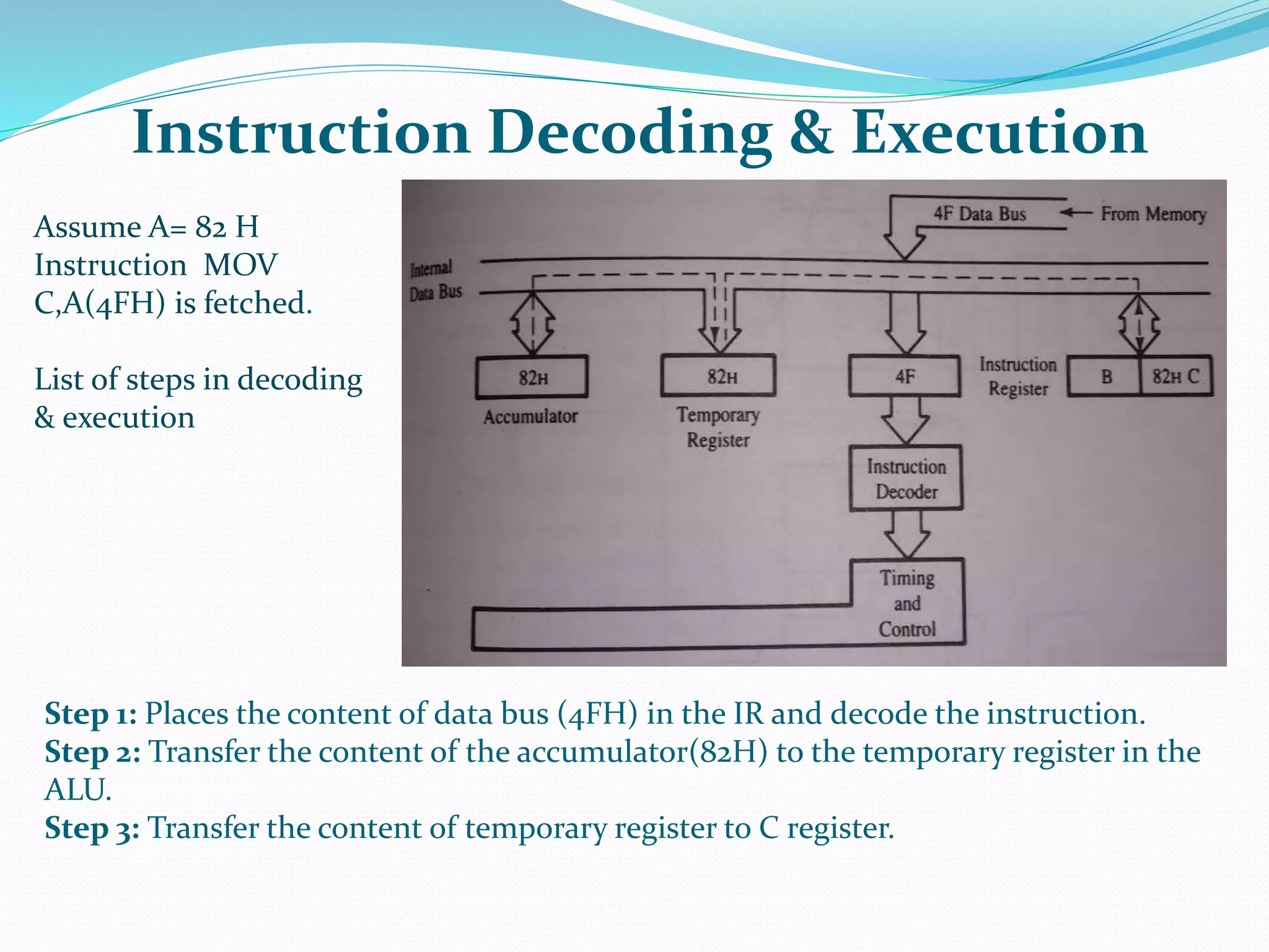
(b.2) Instruction Register: (user not accessible)
When an instruction is fetched from memory, it is loaded in IR. Then transferred to the
decoder for decoding.
It is not programmable and can not be accessed through any instruction.
14](https://image.slidesharecdn.com/chapter1mpuintroduction-170514063435/85/Chapter-1-microprocessor-introduction-14-320.jpg)
![8085 Architecture …… cont….
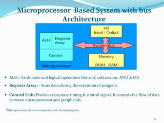
(c) Temporary Register[ W, Z, Temporary data register]
Internally used by the MP(user not accessible)
(c.1) W and Z register:
8 bit capacity
Used to hold temporary addresses during the execution of some
instructions
(c.2) Temporary data register:
8 bit capacity
Used to hold temporary data during ALU operations.
17](https://image.slidesharecdn.com/chapter1mpuintroduction-170514063435/85/Chapter-1-microprocessor-introduction-17-320.jpg)
![8085 Architecture …… cont….
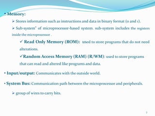
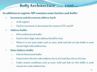
(d) Pointer Register or special purpose [SP, PC]
(d.1) Stack Pointer(SP)
16 bit address which holds the address of the data present at the top of the stack
memory
It is a reserved area of the memory in the RAM to store and retrieve the temporary
information.
Also hold the content of PC when subroutines are used.
When there is a subroutine call or on an interrupt. ie. pushing the return address on a
jump, and retrieving it after the operation is complete to come back to its original
location.
(d.3) Program Counter(PC)
16 bit address used for the execution of program
Contain the address of the next instruction to be executed after fetching the instruction
it is automatically incremented by 1.
Not much use in programming, but as an indicator to user only.
18](https://image.slidesharecdn.com/chapter1mpuintroduction-170514063435/85/Chapter-1-microprocessor-introduction-18-320.jpg)


![8085 Architecture …… cont….
1. Registers Array : 14 register out of which 12 are 8 bit capacity and 2 of 16 bit. Classify into 4 types
(a) General purpose register: (user accessible)
B,C,D,E,H,L are 8 bit register.(can be used singly)
Can also be used for 16-bit register pairs- BC, DE & HL.
Used to store the intermediate data and result
H & L can be used as a data pointer(holds memory address)
(b) Special Purpose Register[A, Instruction Register and Flag]
(b.1) Accumulator (A): (user accessible)
8 bit register
All the ALU operations are performed with reference to the contents of Accumulator.
Result of an operation is stored in A.
Store 8 bit data during I/O transfer
(b.2) Instruction Register: (user not accessible)
When an instruction is fetched from memory, it is loaded in IR. Then transferred to the
decoder for decoding.
It is not programmable and can not be accessed through any instruction.
14](https://image.slidesharecdn.com/chapter1mpuintroduction-170514063435/75/Chapter-1-microprocessor-introduction-14-2048.jpg)
![8085 Architecture …… cont….
(c) Temporary Register[ W, Z, Temporary data register]
Internally used by the MP(user not accessible)
(c.1) W and Z register:
8 bit capacity
Used to hold temporary addresses during the execution of some
instructions
(c.2) Temporary data register:
8 bit capacity
Used to hold temporary data during ALU operations.
17](https://image.slidesharecdn.com/chapter1mpuintroduction-170514063435/75/Chapter-1-microprocessor-introduction-17-2048.jpg)
![8085 Architecture …… cont….
(d) Pointer Register or special purpose [SP, PC]
(d.1) Stack Pointer(SP)
16 bit address which holds the address of the data present at the top of the stack
memory
It is a reserved area of the memory in the RAM to store and retrieve the temporary
information.
Also hold the content of PC when subroutines are used.
When there is a subroutine call or on an interrupt. ie. pushing the return address on a
jump, and retrieving it after the operation is complete to come back to its original
location.
(d.3) Program Counter(PC)
16 bit address used for the execution of program
Contain the address of the next instruction to be executed after fetching the instruction
it is automatically incremented by 1.
Not much use in programming, but as an indicator to user only.
18](https://image.slidesharecdn.com/chapter1mpuintroduction-170514063435/75/Chapter-1-microprocessor-introduction-18-2048.jpg)

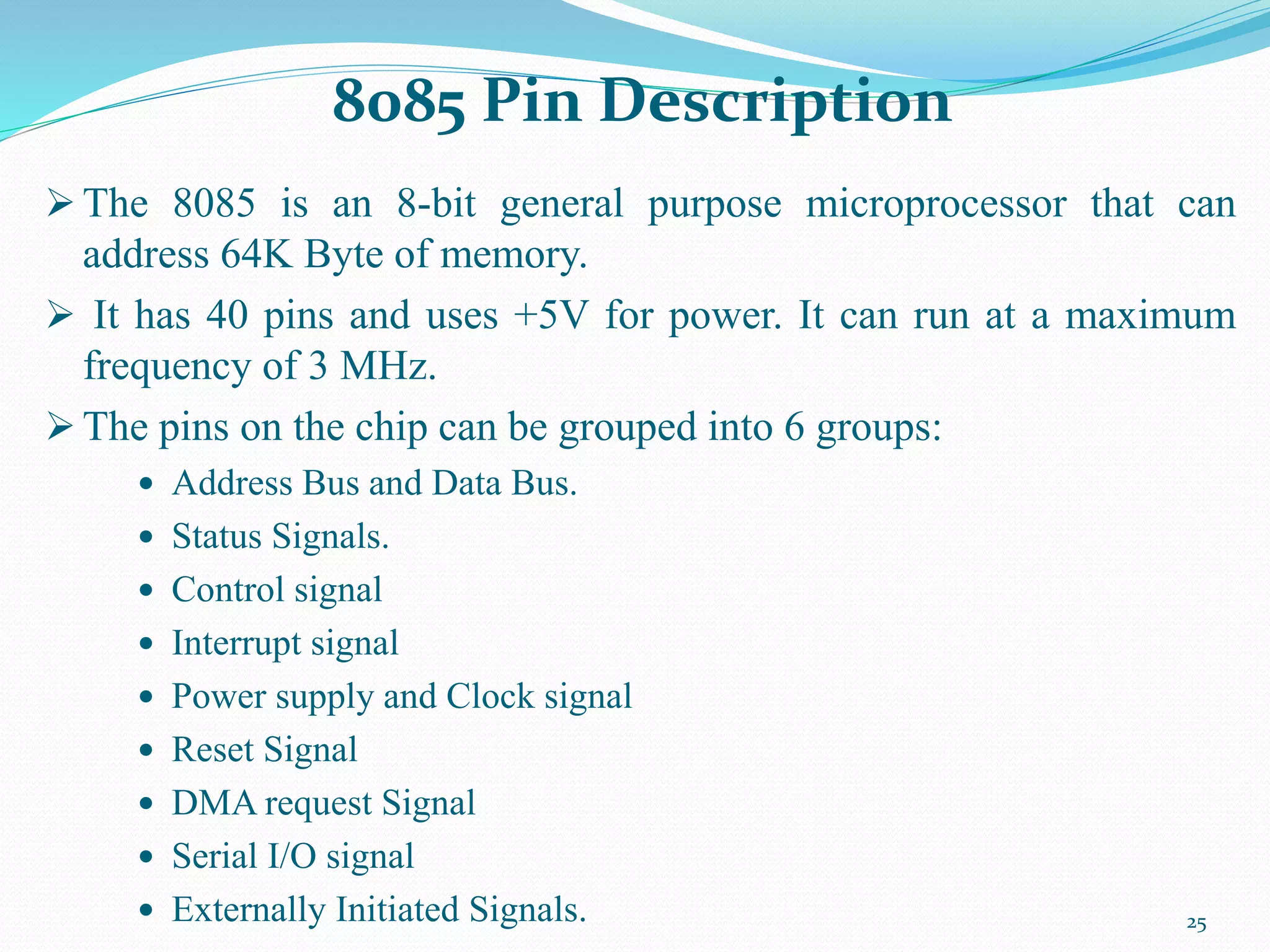
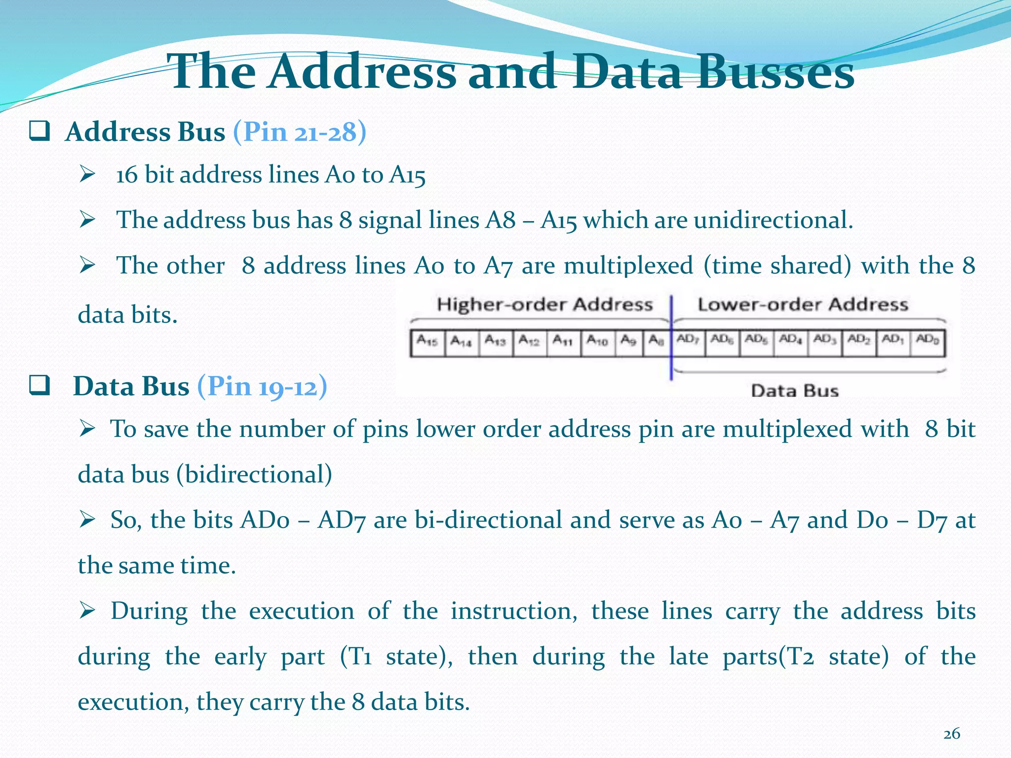
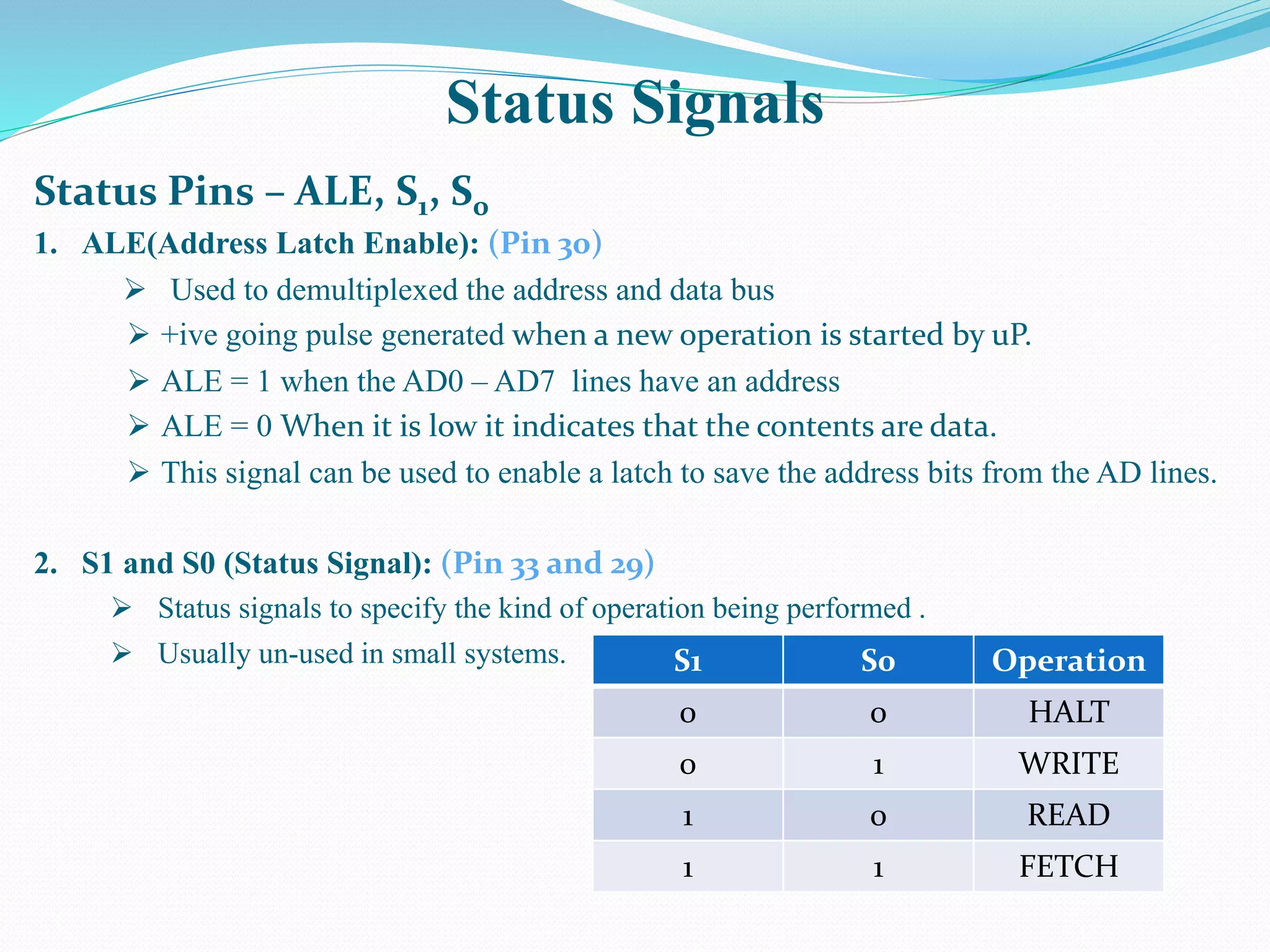
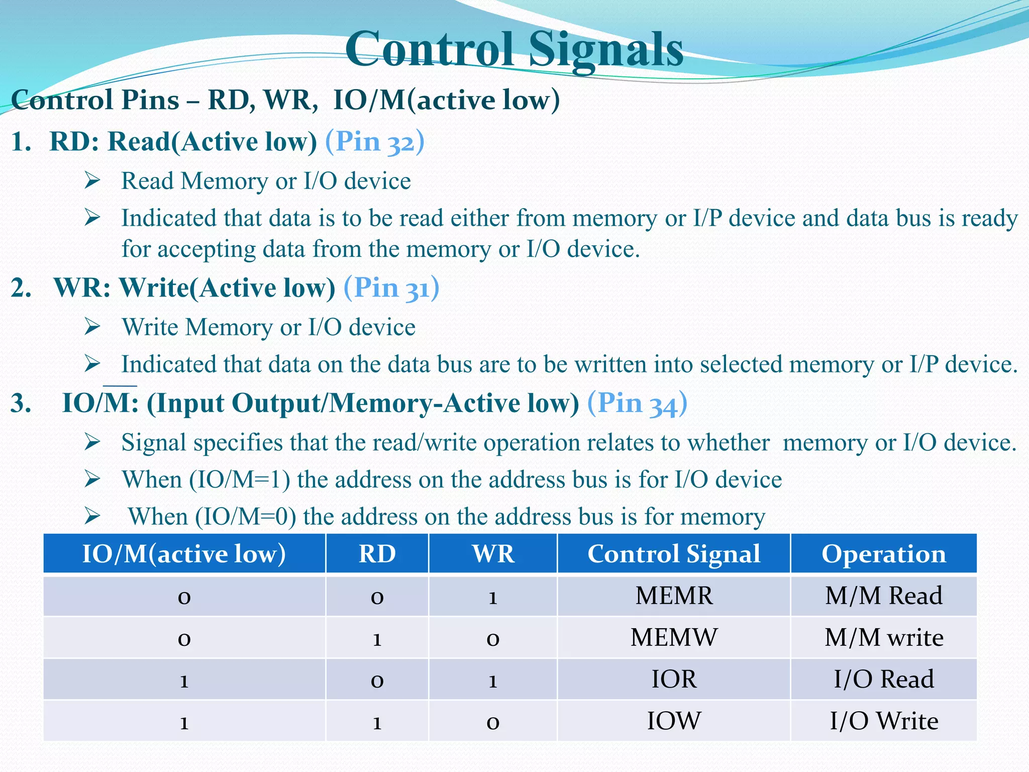


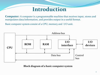
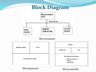
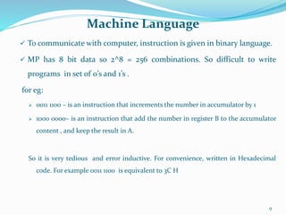
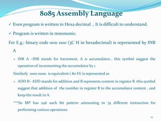
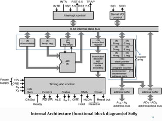
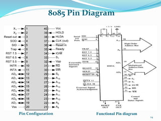
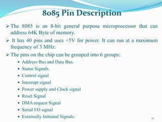
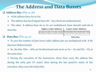
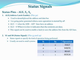
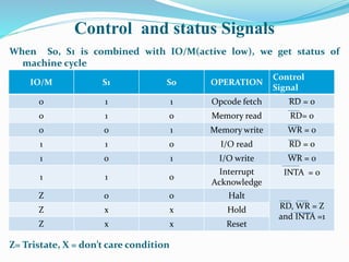
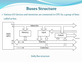
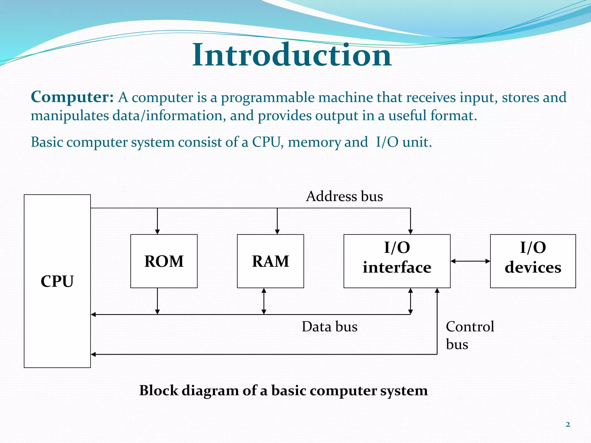
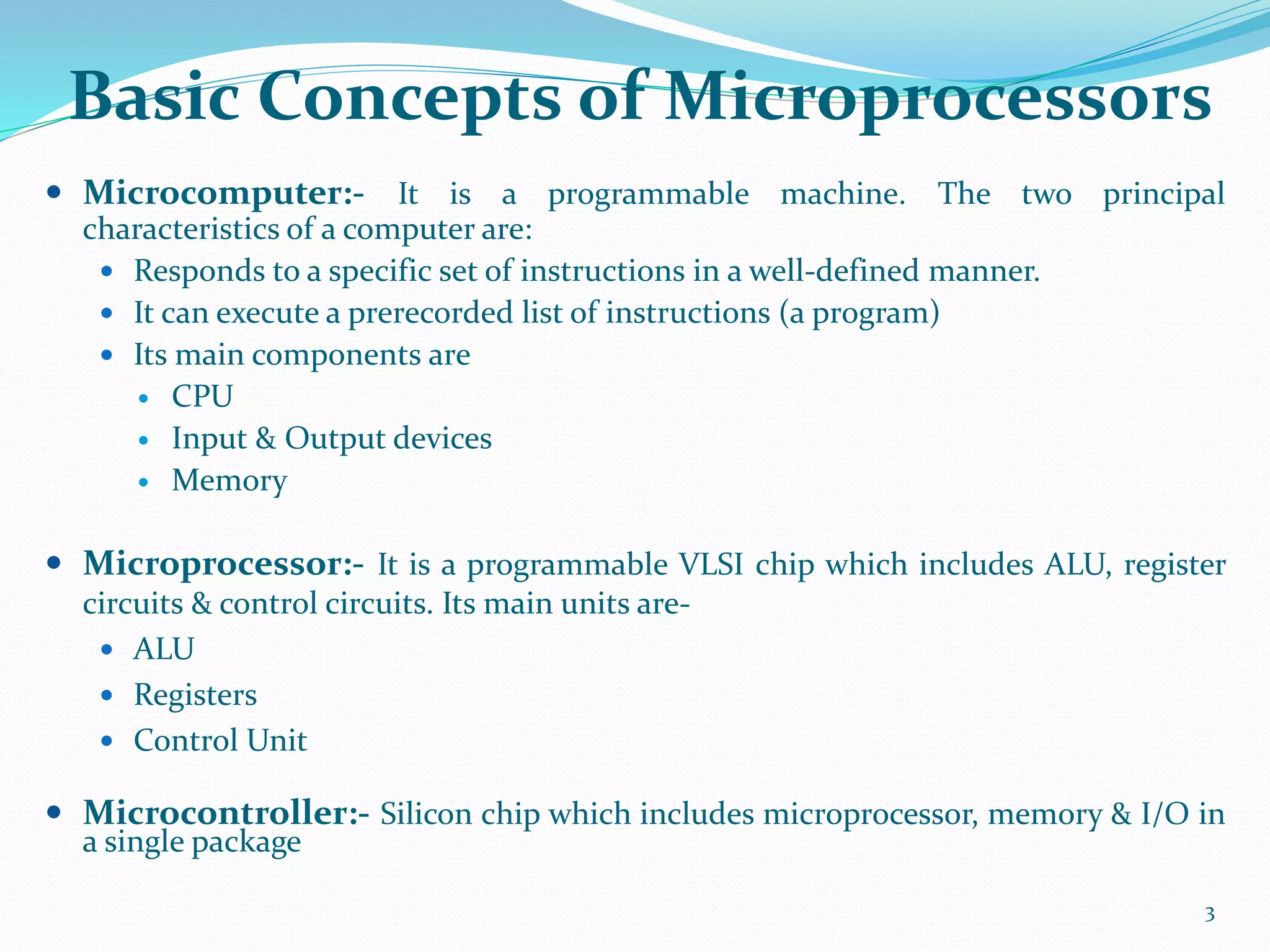
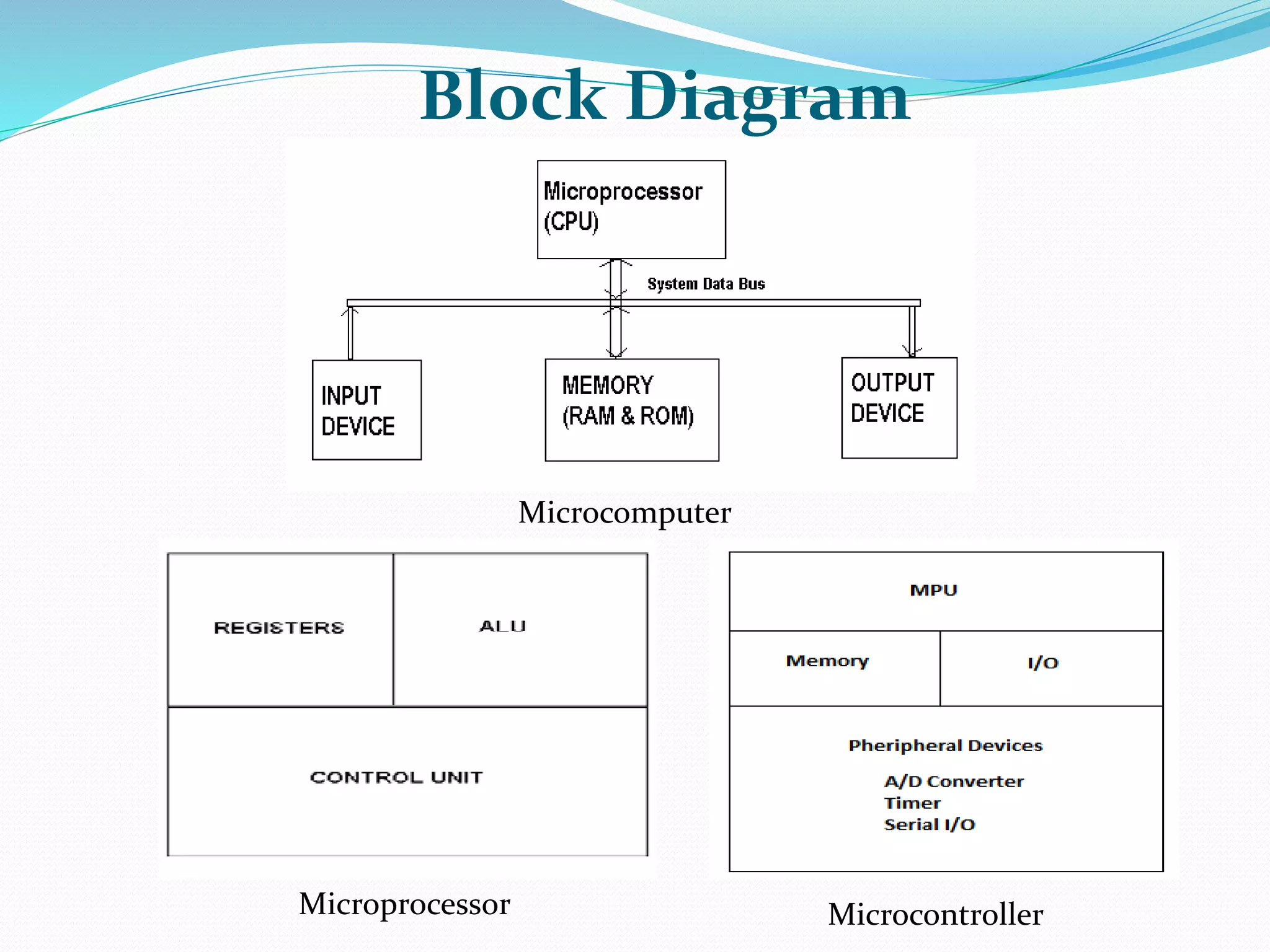
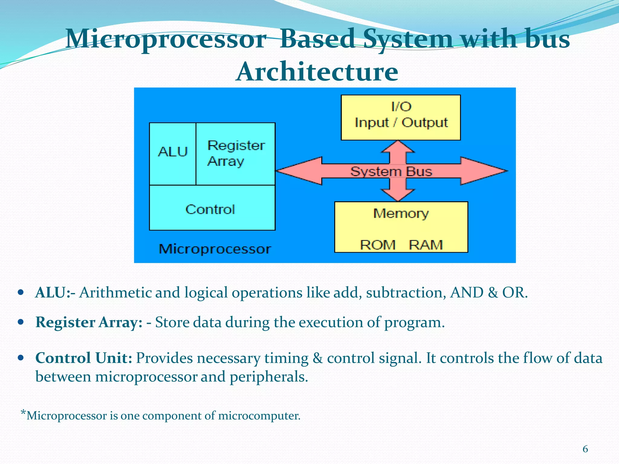
This document provides an introduction and overview of microprocessors. It defines a microprocessor as a programmable VLSI chip that includes an ALU, registers, and control circuits. The document describes the basic components of a computer system including CPU, memory, and I/O. It provides a block diagram of the 8085 microprocessor architecture including its register array, ALU, instruction decoder, interrupt control, and serial I/O control. It also describes the address bus, data bus, status signals, control signals, and pin configuration of the 8085 microprocessor.


