2
OUTLINE
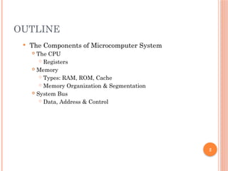
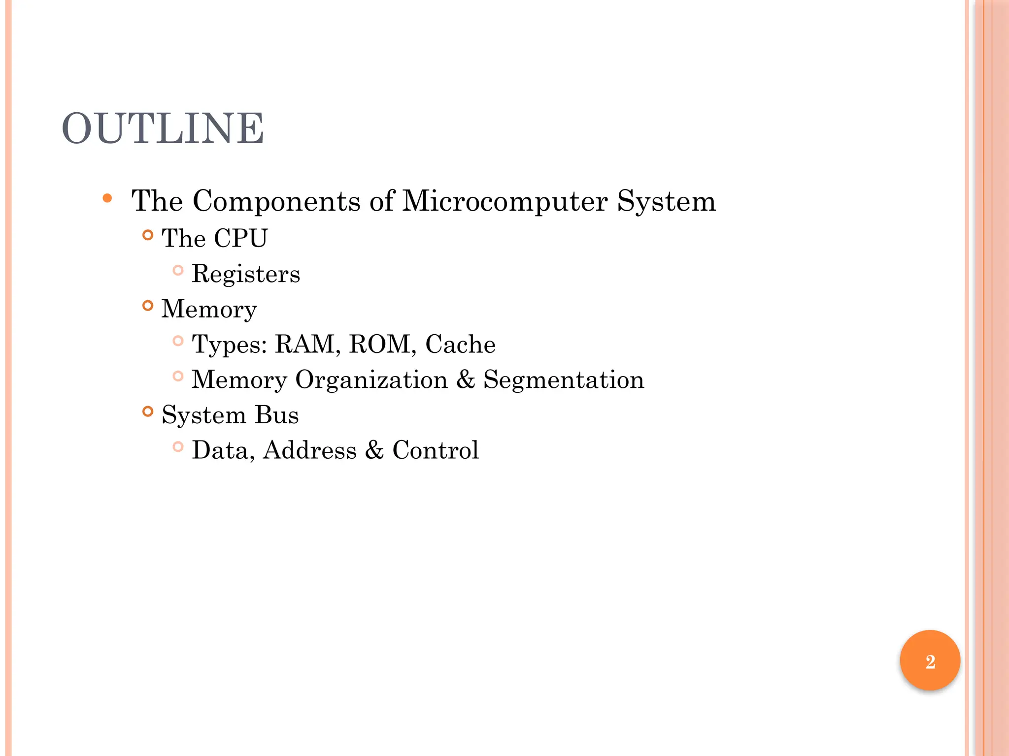
The Componentsof Microcomputer System
The CPU
Registers
Memory
Types: RAM, ROM, Cache
Memory Organization & Segmentation
System Bus
Data, Address & Control
3.
3
REFERENCES
Chapter 1,Ytha Yu and Charles Marut, “Assembly Language
Programming and Organization of IBM PC”
Chapter 3, William Stallings, “Computer Organization &
Architecture”
Chapter 2, Subrata Ghoshal, “Computer Organization &
Architecture”
5
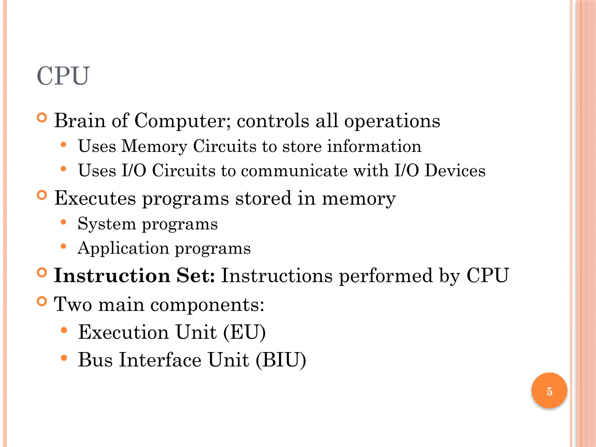
CPU
Brain ofComputer; controls all operations
Uses Memory Circuits to store information
Uses I/O Circuits to communicate with I/O Devices
Executes programs stored in memory
System programs
Application programs
Instruction Set: Instructions performed by CPU
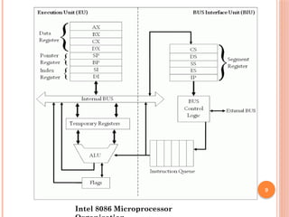
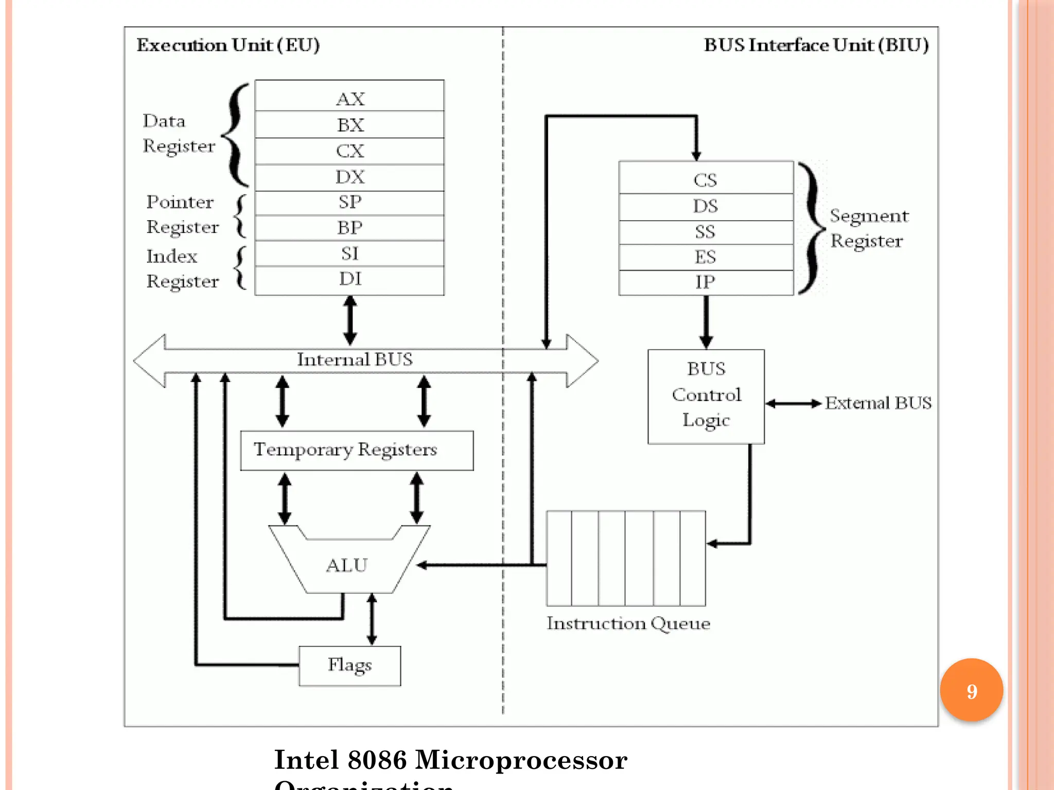
Two main components:
Execution Unit (EU)
Bus Interface Unit (BIU)
6.
6
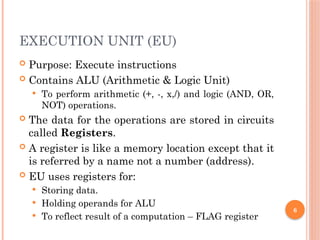
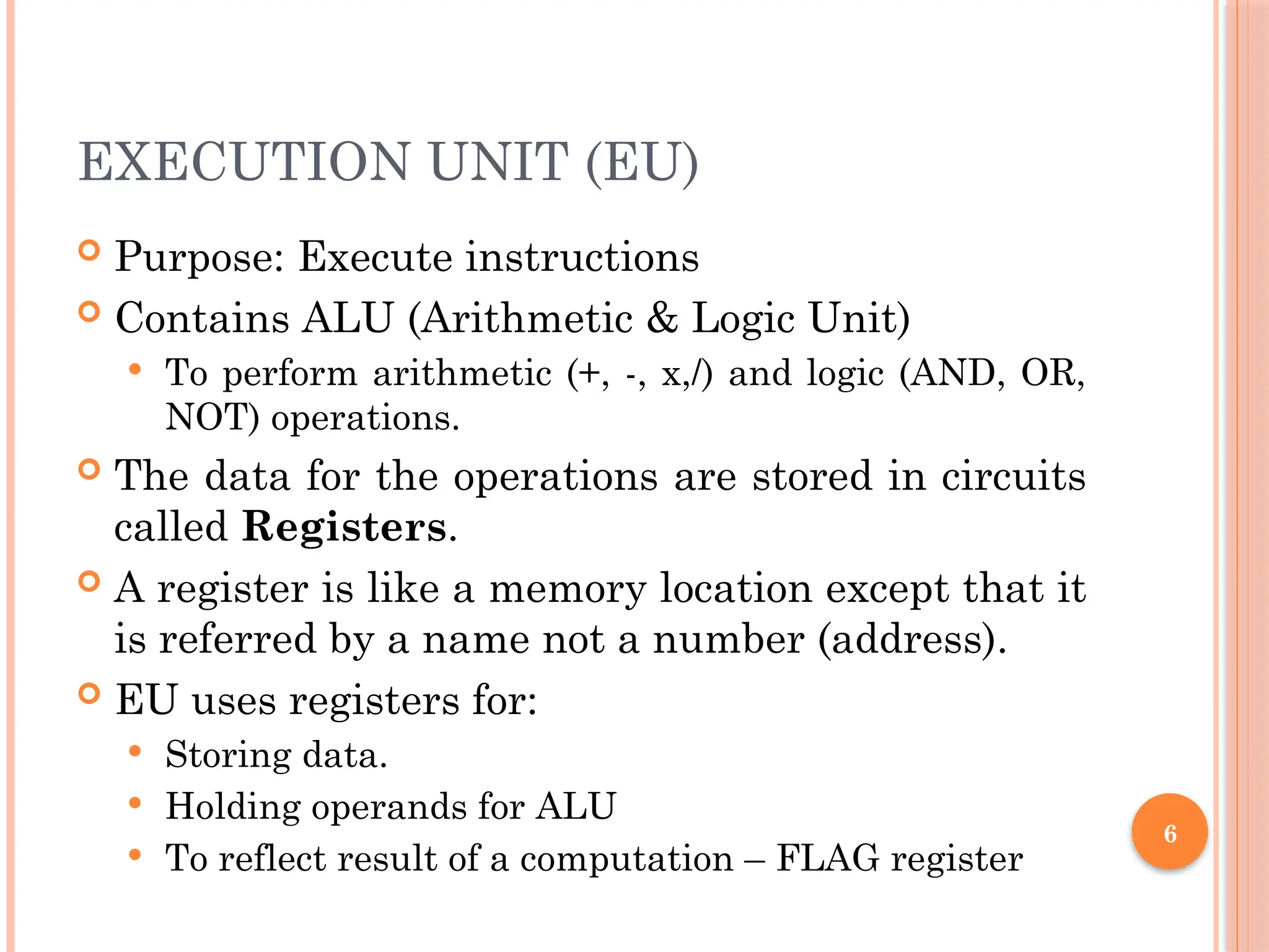
EXECUTION UNIT (EU)
Purpose: Execute instructions
Contains ALU (Arithmetic & Logic Unit)
To perform arithmetic (+, -, x,/) and logic (AND, OR,
NOT) operations.
The data for the operations are stored in circuits
called Registers.
A register is like a memory location except that it
is referred by a name not a number (address).
EU uses registers for:
Storing data.
Holding operands for ALU
To reflect result of a computation – FLAG register
7.
7
BUS INTERFACE UNIT(BIU)
Facilitates communication between the EU and
the memory or I/O circuits.
Responsible for transmitting address, data and
control signals on the buses.
8.
8
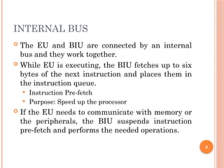
INTERNAL BUS
TheEU and BIU are connected by an internal
bus and they work together.
While EU is executing, the BIU fetches up to six
bytes of the next instruction and places them in
the instruction queue.
Instruction Pre-fetch
Purpose: Speed up the processor
If the EU needs to communicate with memory or
the peripherals, the BIU suspends instruction
pre-fetch and performs the needed operations.
REGISTERS
Registers arehigh-speed storage locations inside the
microprocessor.
Designed to be accessed at much higher speed than
conventional memory.
Registers are classified according to the functions they
perform.
General Types of Registers:
Data Registers: To hold data for an operation.
Address Registers: To hold the address of an instruction or
data.
Status/Flag Register: keeps the current status of the
processor or result of an arithmetic operation.
11
12.
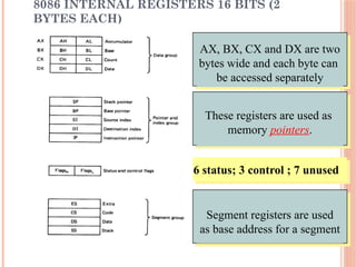
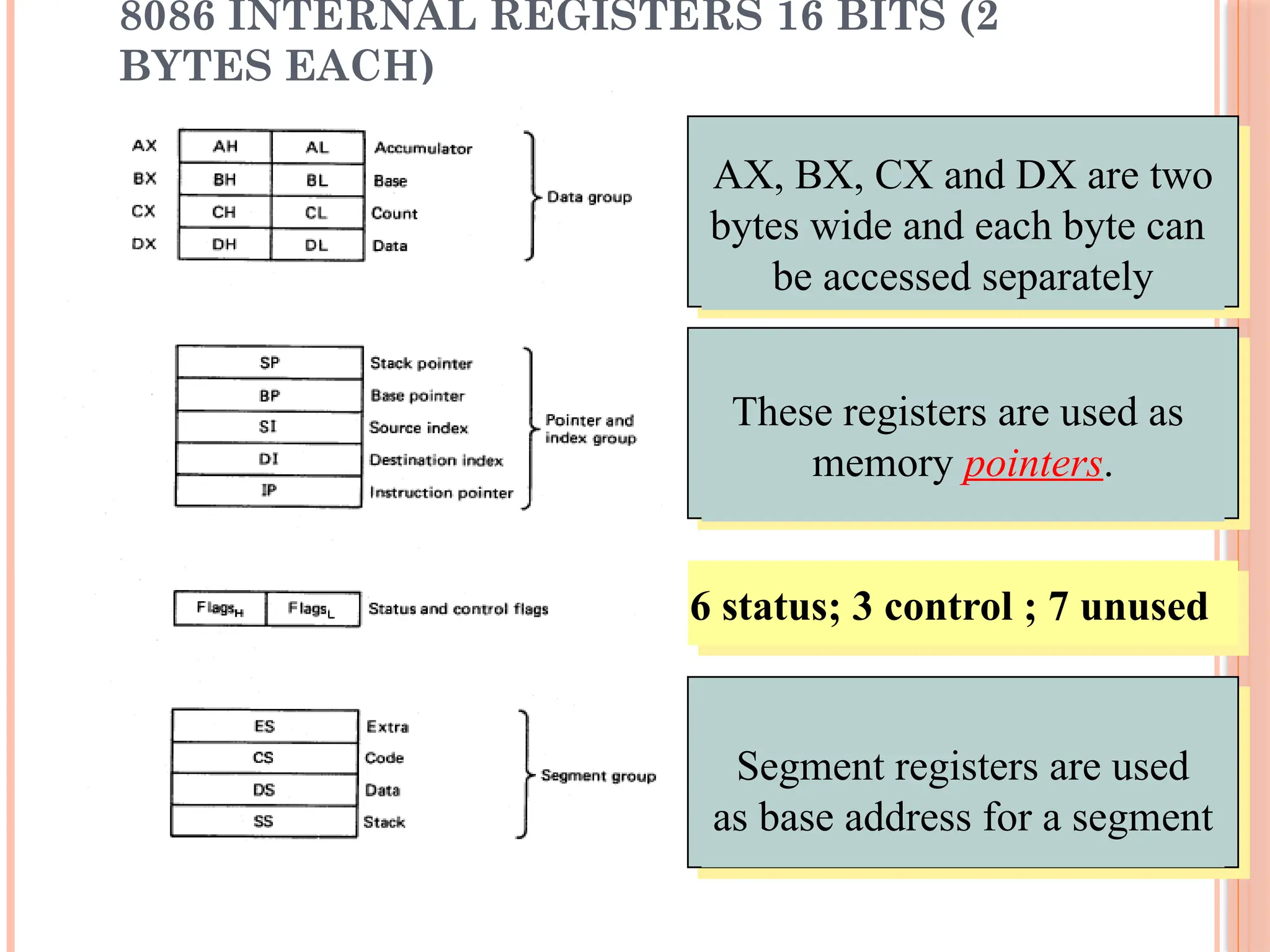
8086 INTERNAL REGISTERS16 BITS (2
BYTES EACH)
12
AX, BX, CX and DX are two
bytes wide and each byte can
be accessed separately
These registers are used as
memory pointers.
Segment registers are used
as base address for a segment
6 status; 3 control ; 7 unused
13.
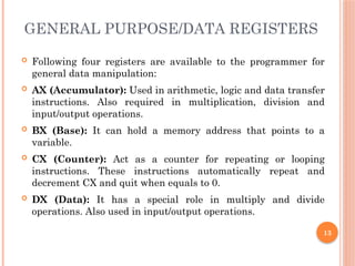
GENERAL PURPOSE/DATA REGISTERS
Following four registers are available to the programmer for
general data manipulation:
AX (Accumulator): Used in arithmetic, logic and data transfer
instructions. Also required in multiplication, division and
input/output operations.
BX (Base): It can hold a memory address that points to a
variable.
CX (Counter): Act as a counter for repeating or looping
instructions. These instructions automatically repeat and
decrement CX and quit when equals to 0.
DX (Data): It has a special role in multiply and divide
operations. Also used in input/output operations.
13
14.
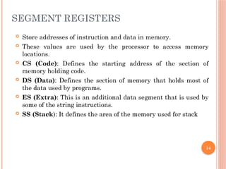
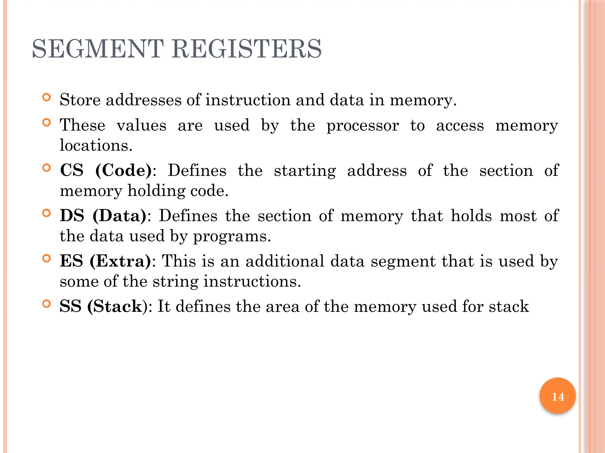
SEGMENT REGISTERS
Storeaddresses of instruction and data in memory.
These values are used by the processor to access memory
locations.
CS (Code): Defines the starting address of the section of
memory holding code.
DS (Data): Defines the section of memory that holds most of
the data used by programs.
ES (Extra): This is an additional data segment that is used by
some of the string instructions.
SS (Stack): It defines the area of the memory used for stack
14
15.
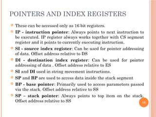
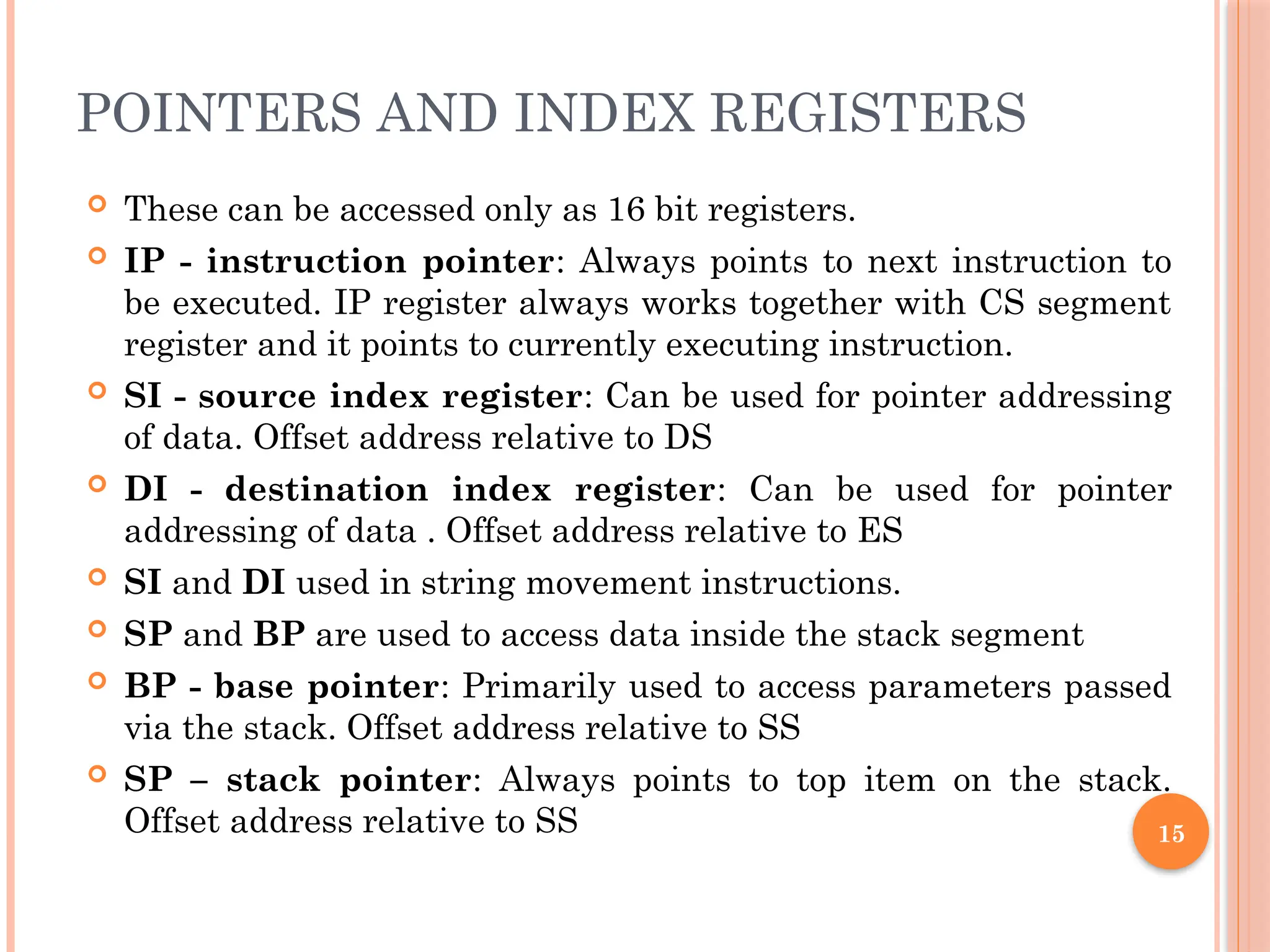
POINTERS AND INDEXREGISTERS
These can be accessed only as 16 bit registers.
IP - instruction pointer: Always points to next instruction to
be executed. IP register always works together with CS segment
register and it points to currently executing instruction.
SI - source index register: Can be used for pointer addressing
of data. Offset address relative to DS
DI - destination index register: Can be used for pointer
addressing of data . Offset address relative to ES
SI and DI used in string movement instructions.
SP and BP are used to access data inside the stack segment
BP - base pointer: Primarily used to access parameters passed
via the stack. Offset address relative to SS
SP – stack pointer: Always points to top item on the stack.
Offset address relative to SS 15
16.
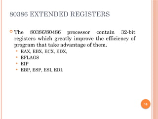
80386 EXTENDED REGISTERS
The 80386/80486 processor contain 32-bit
registers which greatly improve the efficiency of
program that take advantage of them.
EAX, EBX, ECX, EDX,
EFLAGS
EIP
EBP, ESP, ESI, EDI.
16
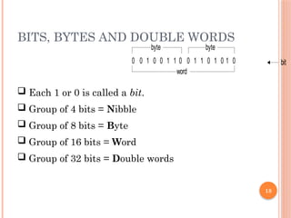
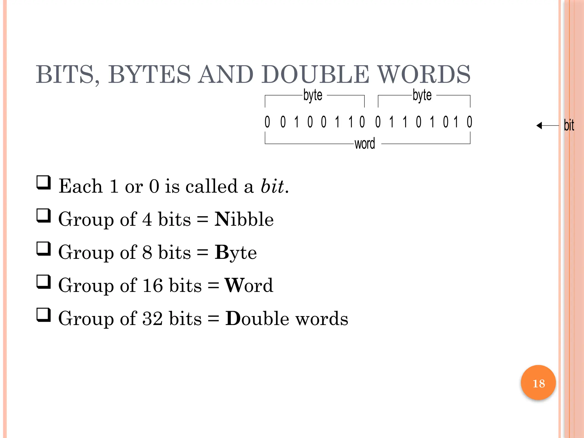
18
byte byte
word
bit
0
1 0
0
01
0 1 1
0 1 0
1
0 1
0
Each 1 or 0 is called a bit.
Group of 4 bits = Nibble
Group of 8 bits = Byte
Group of 16 bits = Word
Group of 32 bits = Double words
BITS, BYTES AND DOUBLE WORDS
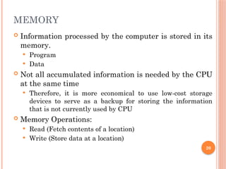
MEMORY
Information processedby the computer is stored in its
memory.
Program
Data
Not all accumulated information is needed by the CPU
at the same time
Therefore, it is more economical to use low-cost storage
devices to serve as a backup for storing the information
that is not currently used by CPU
Memory Operations:
Read (Fetch contents of a location)
Write (Store data at a location)
20
22
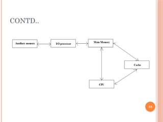
CONTD..
The memoryunit that directly communicate with
CPU is called the main memory
Devices that provide backup storage are called
auxiliary memory
The main memory occupies a central position by being
able to communicate directly with the CPU and with
auxiliary memory devices through an I/O processor
A special very-high-speed memory called cache is
used to increase the speed of processing by making
current programs and data available to the CPU at a
rapid rate
24
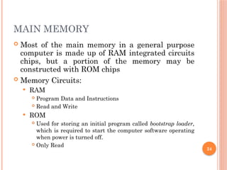
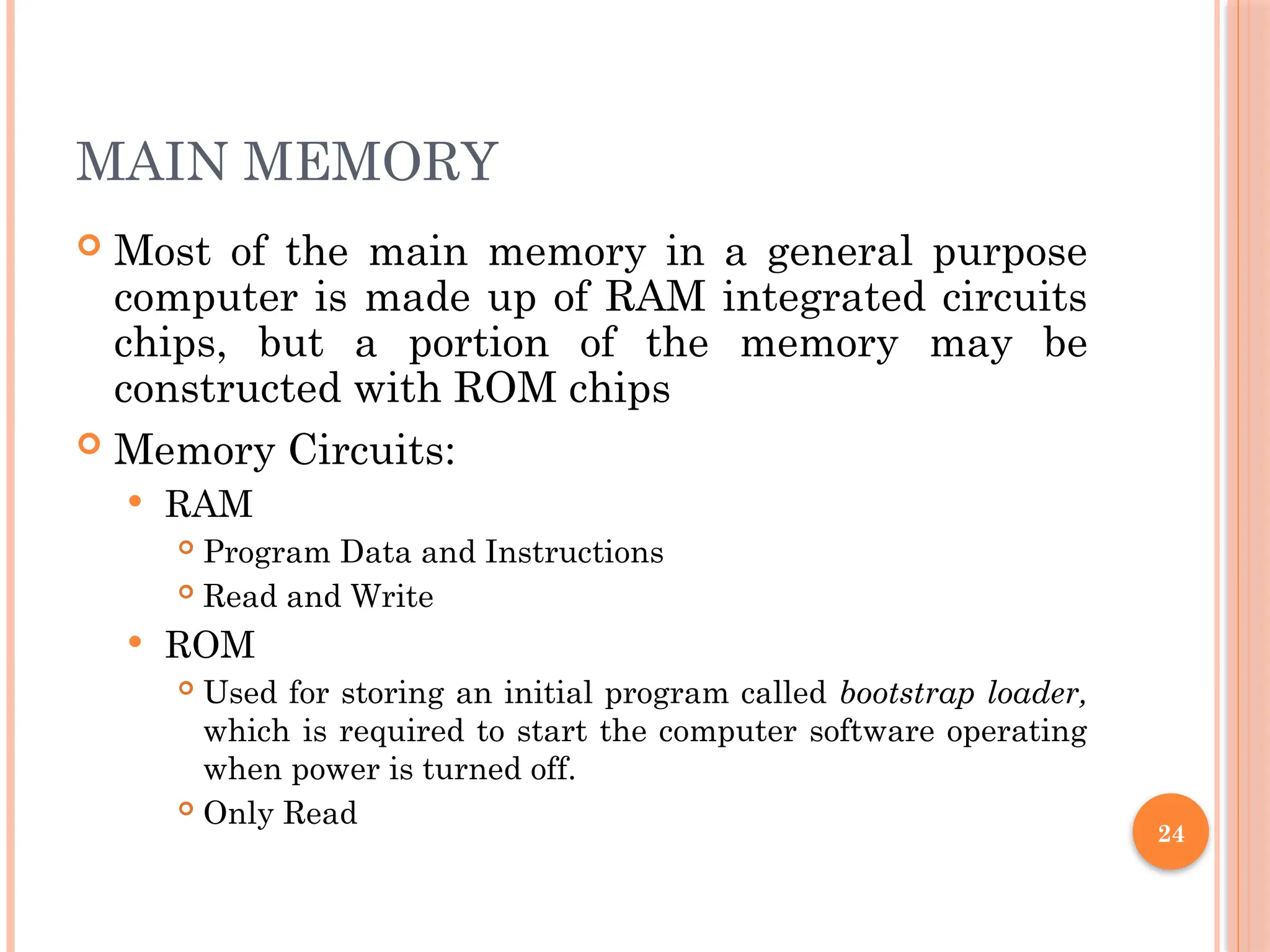
MAIN MEMORY
Mostof the main memory in a general purpose
computer is made up of RAM integrated circuits
chips, but a portion of the memory may be
constructed with ROM chips
Memory Circuits:
RAM
Program Data and Instructions
Read and Write
ROM
Used for storing an initial program called bootstrap loader,
which is required to start the computer software operating
when power is turned off.
Only Read
25.
25
CACHE
A specialvery-high-speed memory called cache
is used to increase the speed of processing by
making current programs and data available to
the CPU at a rapid rate.
To reduce memory access time thus program
execution time.
26.
MEMORY ORGANIZATION
Memoryis organized into a collection of bytes.
Each byte is identified by a number – Address
Number of bits in an address depends on the
processor
Example:- Intel 8086: 20-bit address, Intel 80286: 24-
bit address
Data stored in a memory byte – Contents
26
27.
27
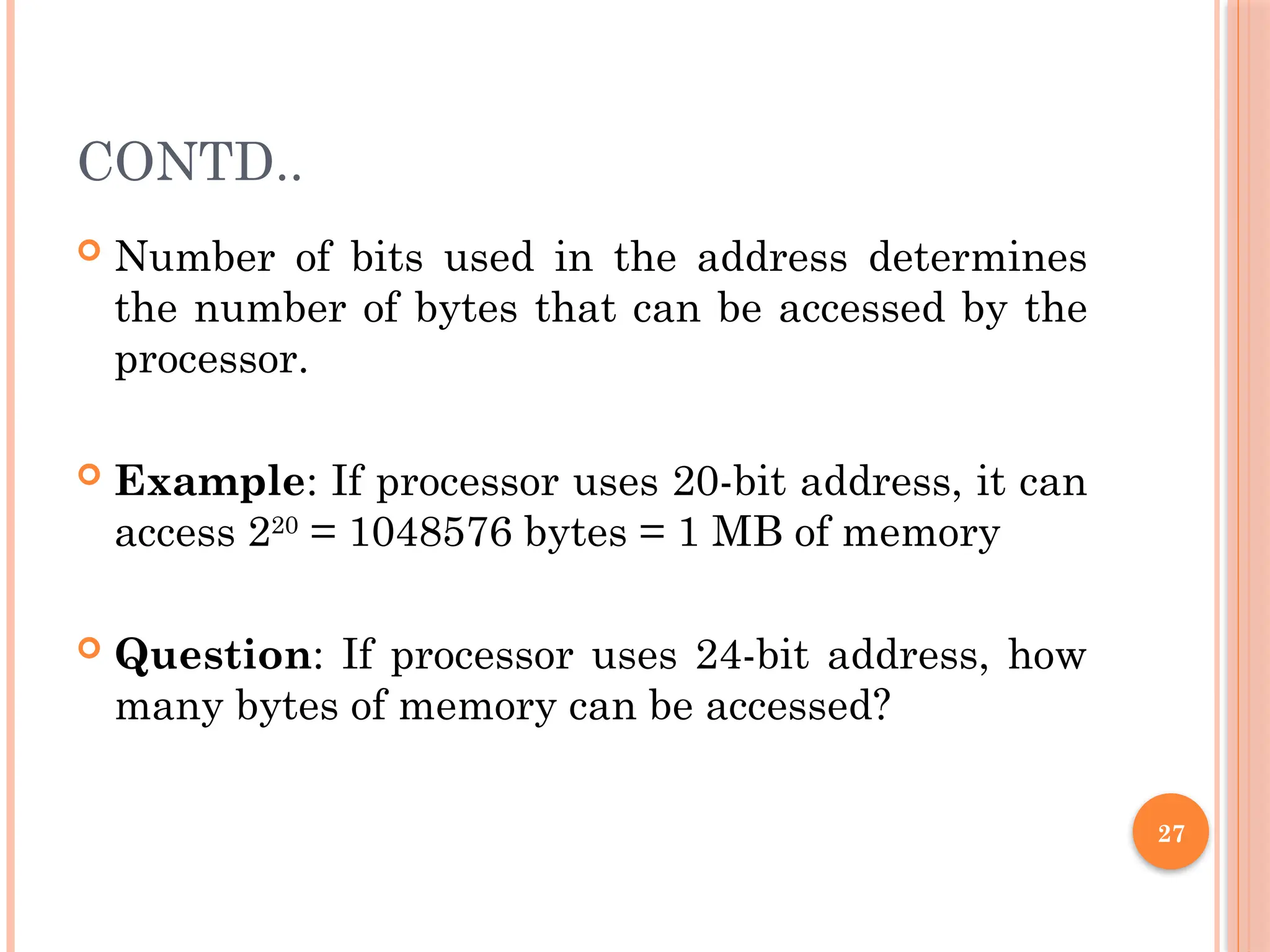
CONTD..
Number ofbits used in the address determines
the number of bytes that can be accessed by the
processor.
Example: If processor uses 20-bit address, it can
access 220
= 1048576 bytes = 1 MB of memory
Question: If processor uses 24-bit address, how
many bytes of memory can be accessed?
28.
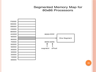
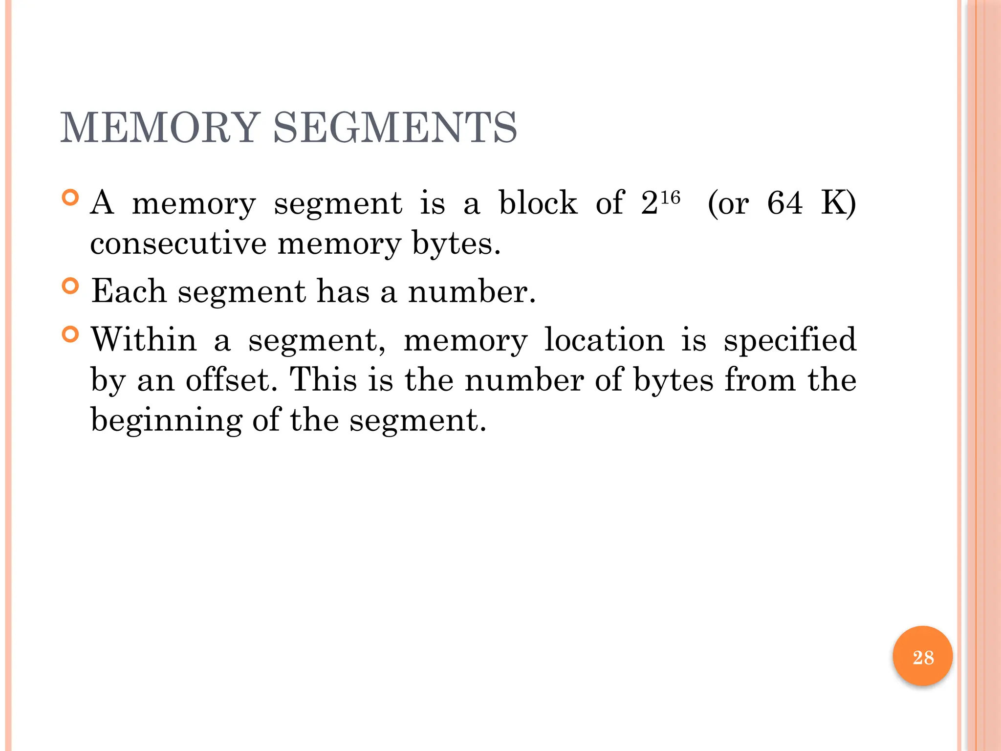
MEMORY SEGMENTS
Amemory segment is a block of 216
(or 64 K)
consecutive memory bytes.
Each segment has a number.
Within a segment, memory location is specified
by an offset. This is the number of bytes from the
beginning of the segment.
28
31
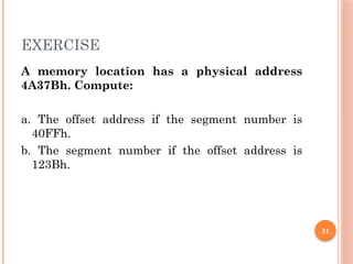
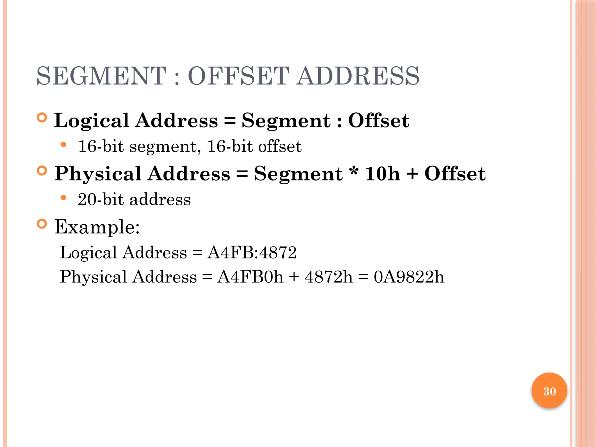
EXERCISE
A memory locationhas a physical address
4A37Bh. Compute:
a. The offset address if the segment number is
40FFh.
b. The segment number if the offset address is
123Bh.
32.
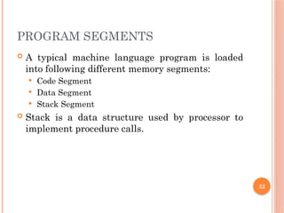
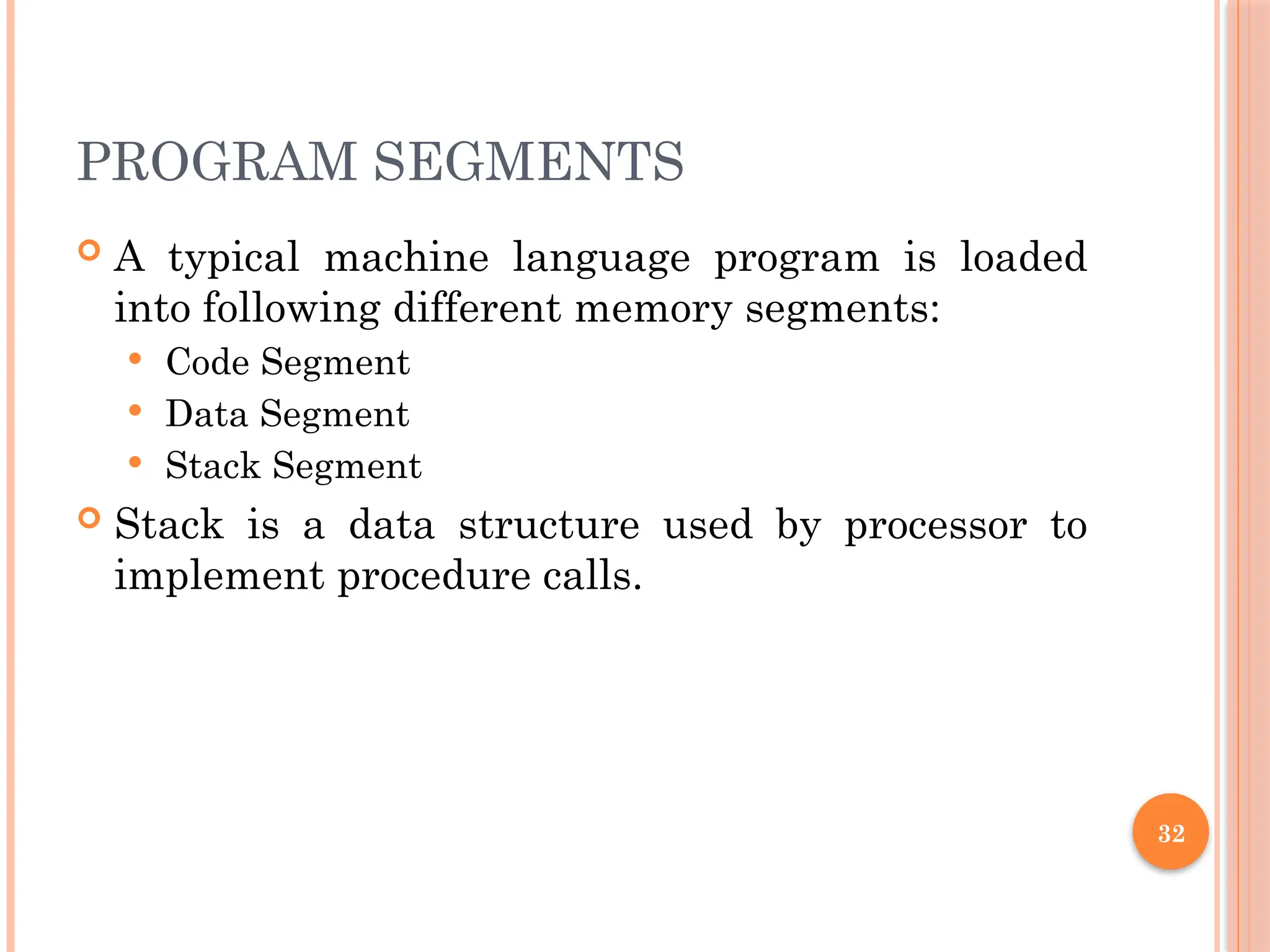
PROGRAM SEGMENTS
Atypical machine language program is loaded
into following different memory segments:
Code Segment
Data Segment
Stack Segment
Stack is a data structure used by processor to
implement procedure calls.
32
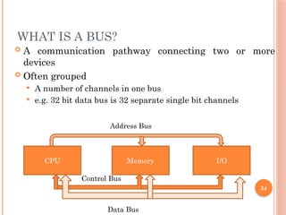
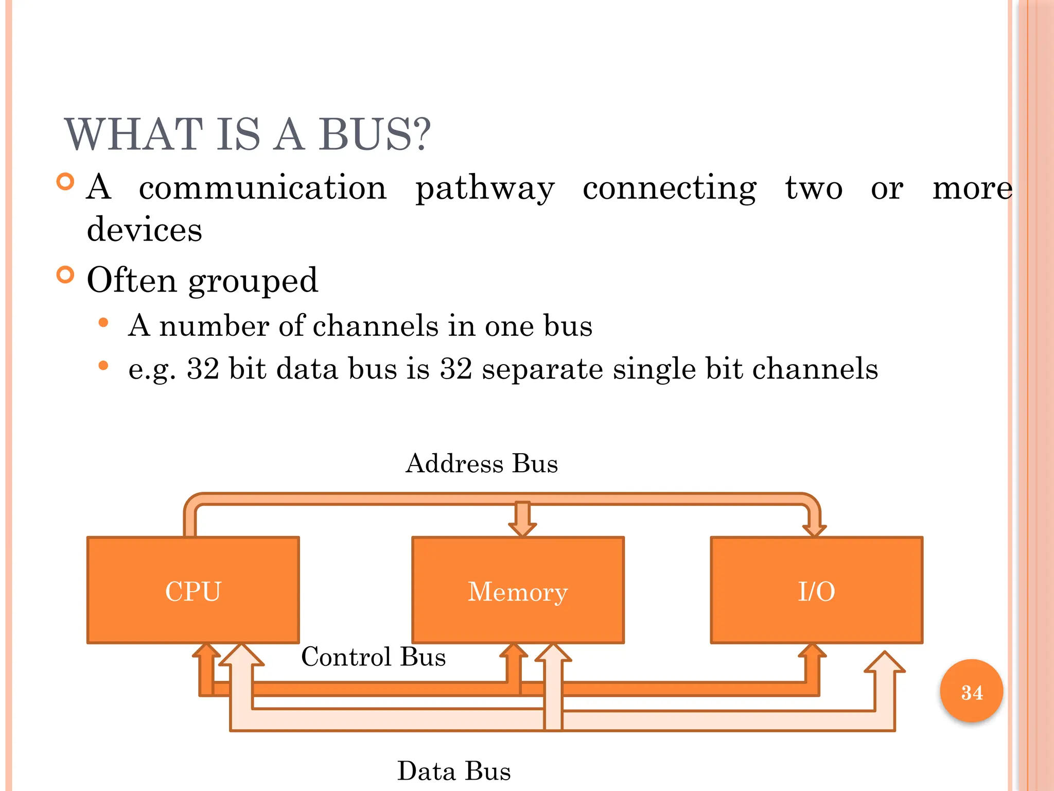
WHAT IS ABUS?
A communication pathway connecting two or more
devices
Often grouped
A number of channels in one bus
e.g. 32 bit data bus is 32 separate single bit channels
34
CPU Memory I/O
Address Bus
Control Bus
Data Bus
35.
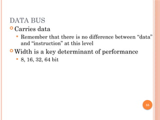
DATA BUS
Carriesdata
Remember that there is no difference between “data”
and “instruction” at this level
Width is a key determinant of performance
8, 16, 32, 64 bit
35
36.
ADDRESS BUS
Identifythe source or destination of data
e.g. CPU needs to read an instruction (data) from a given
location in memory
Bus width determines maximum memory capacity of
system
e.g. 8080 has 16 bit address bus giving 64k address space
36
37.
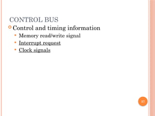
CONTROL BUS
Controland timing information
Memory read/write signal
Interrupt request
Clock signals
37
38.
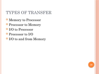
TYPES OF TRANSFER
Memory to Processor
Processor to Memory
I/O to Processor
Processor to I/O
I/O to and from Memory
38
39.
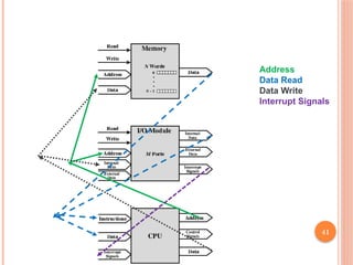
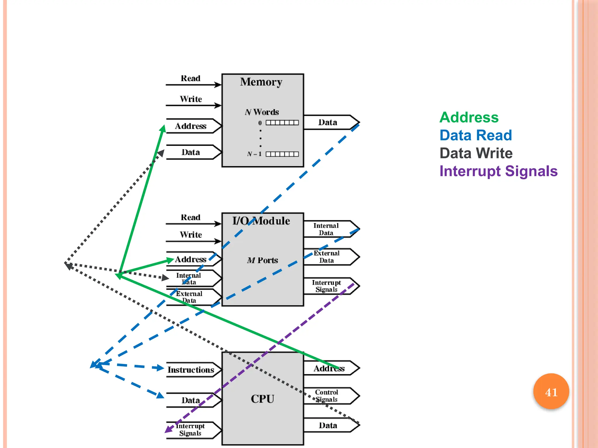
INTERCONNECTION STRUCTURE
Memory
N words of equal length, each word having a unique
address
Unit of Transfer (read/Write): Word
Operation: Read/Write indicated by Control Signal
Location of operation specified by an address
I/O Module
Two operations: read and write
May control other external devices
Port: interface between I/O module and device
Able to send interrupt signal to CPU
39
40.
CONTD..
CPU
Readsin instruction and data
Writes out data
Uses control signal to control all operations
Receives interrupt signal
40