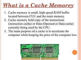
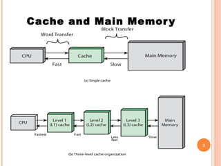
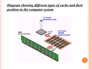
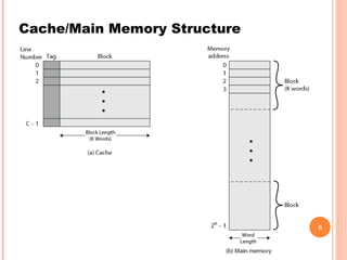
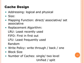
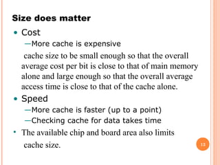
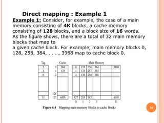
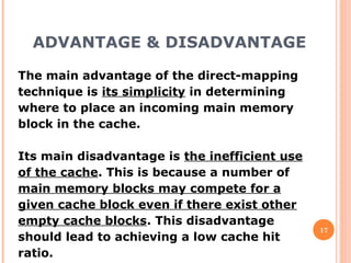
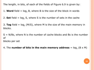
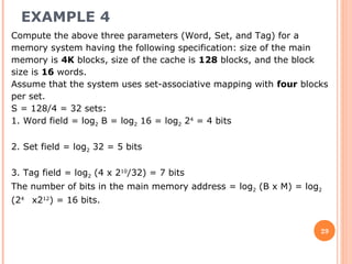
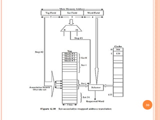
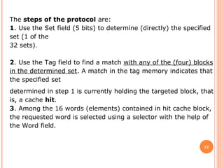
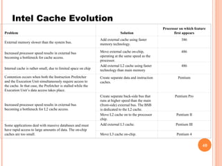
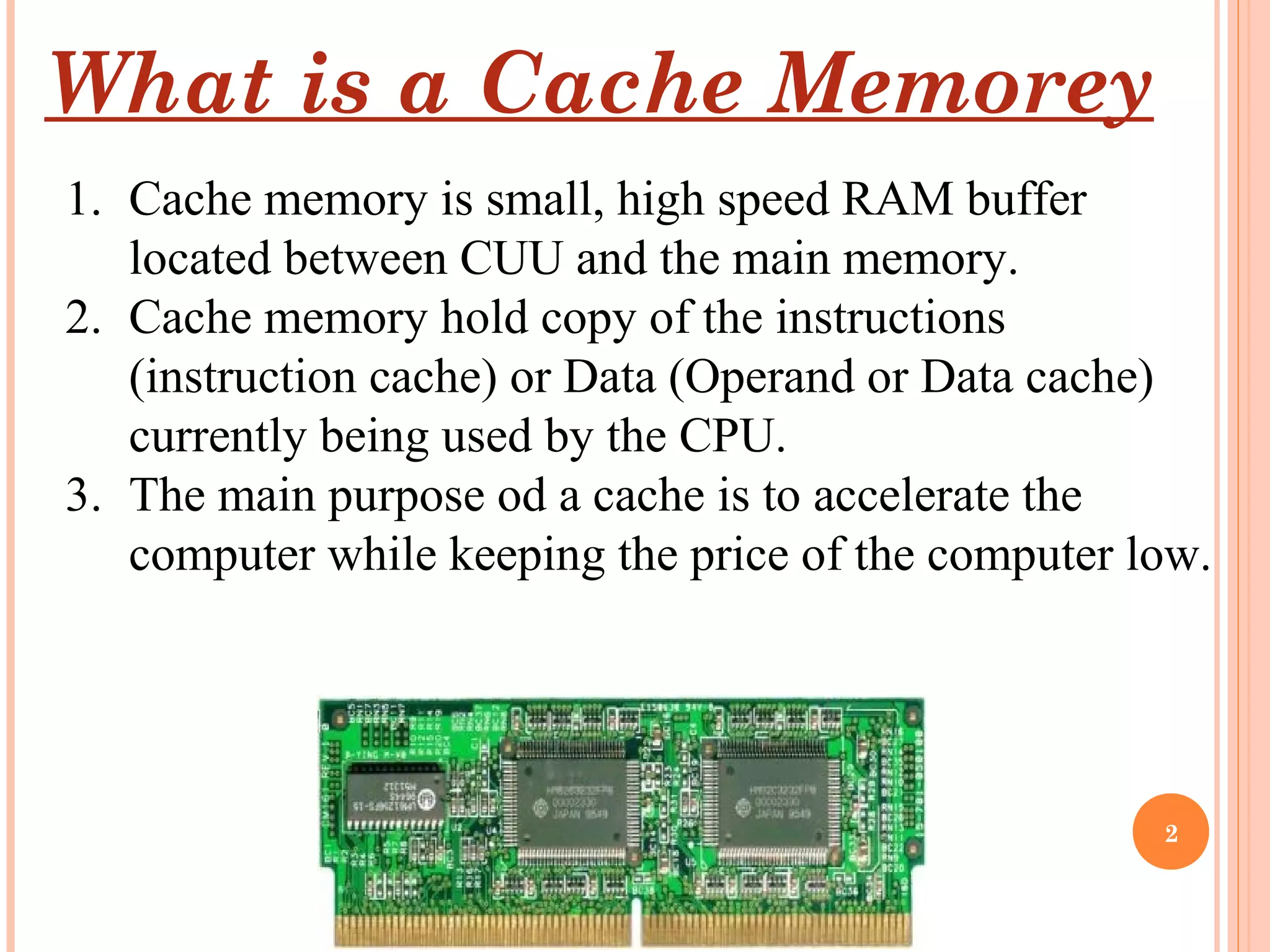
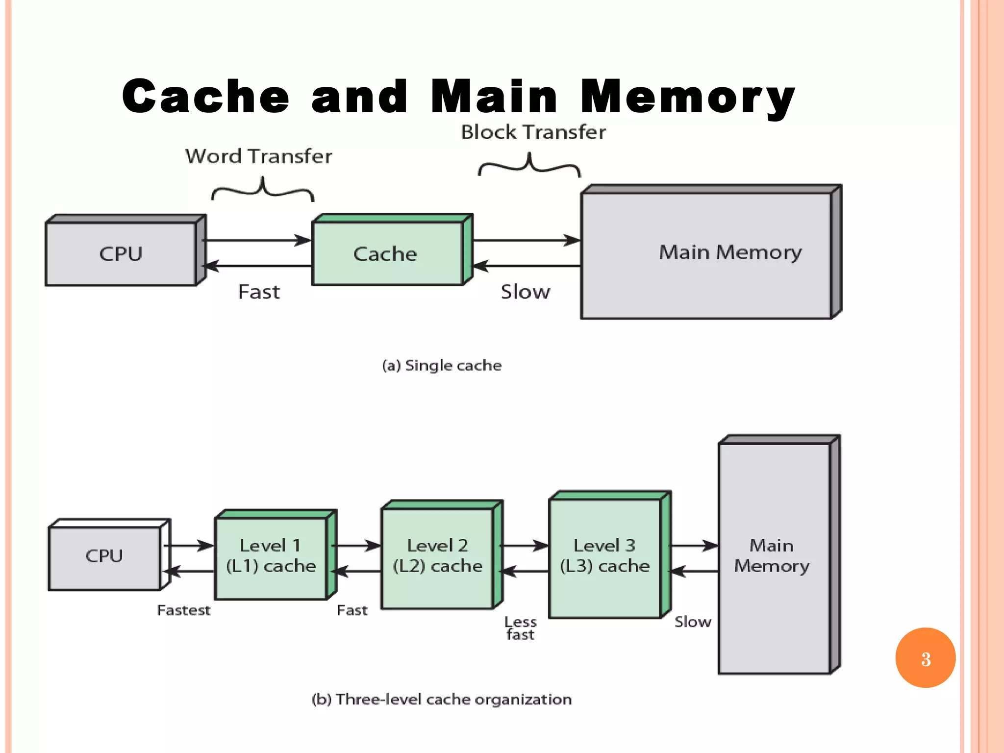
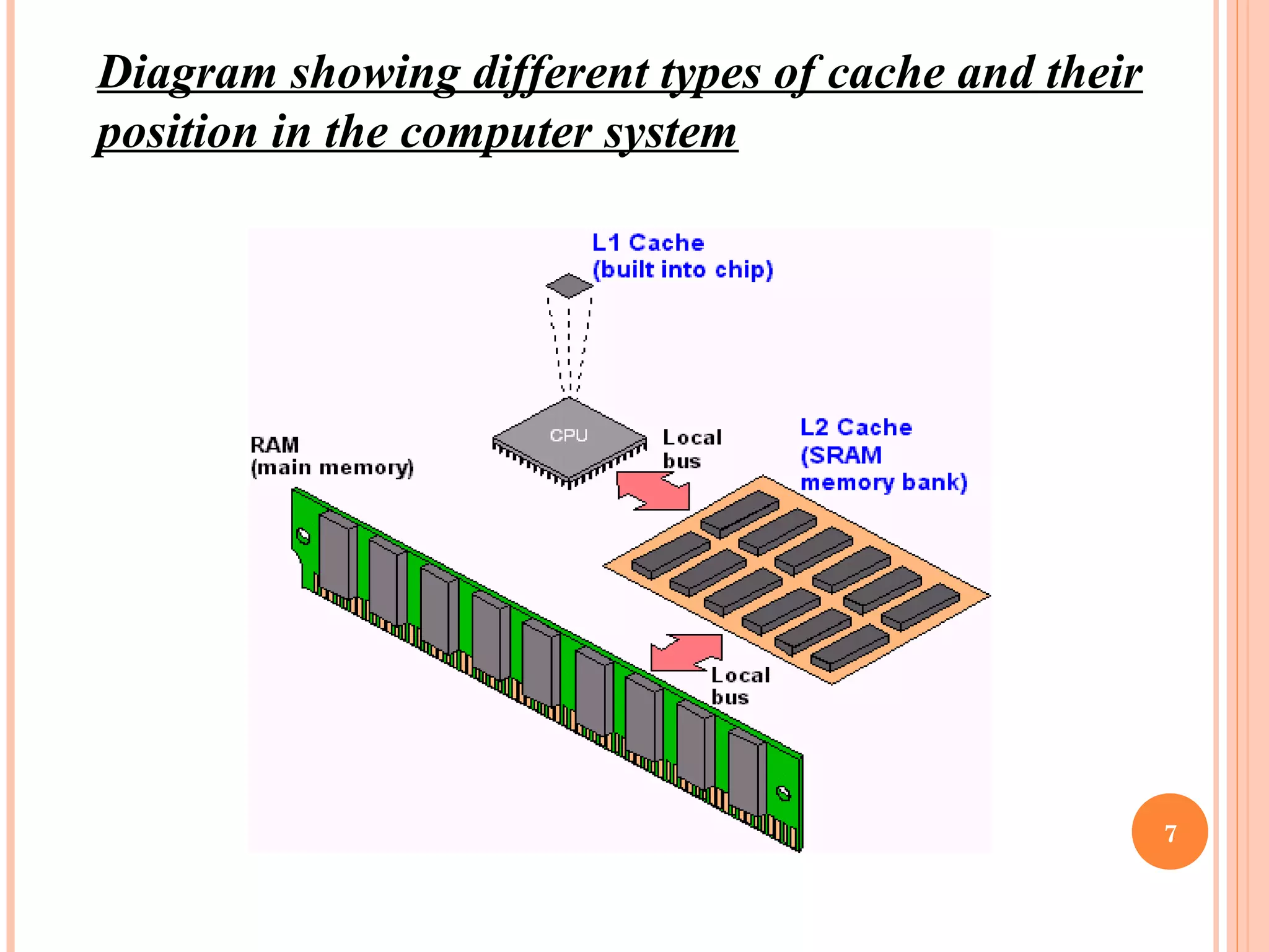
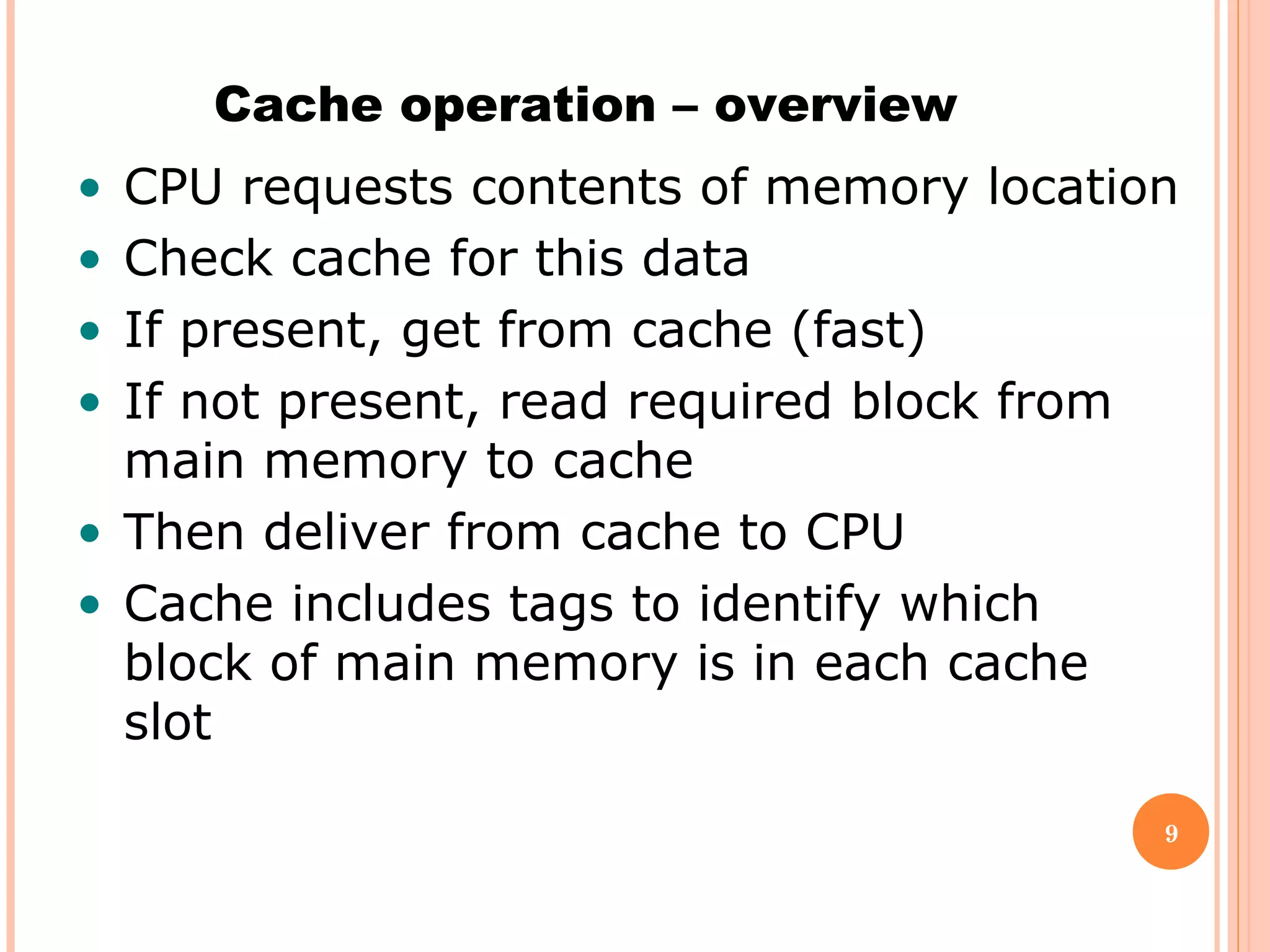
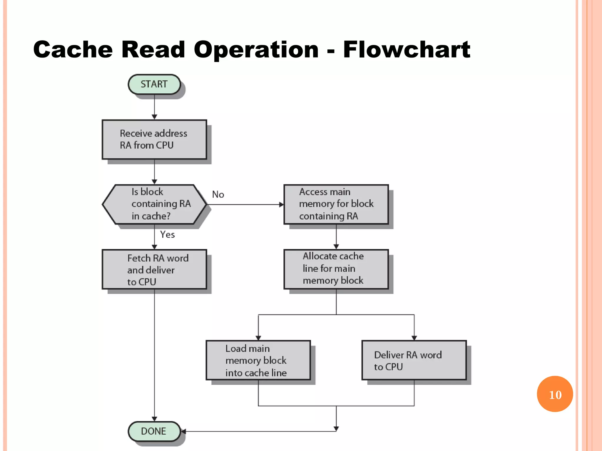
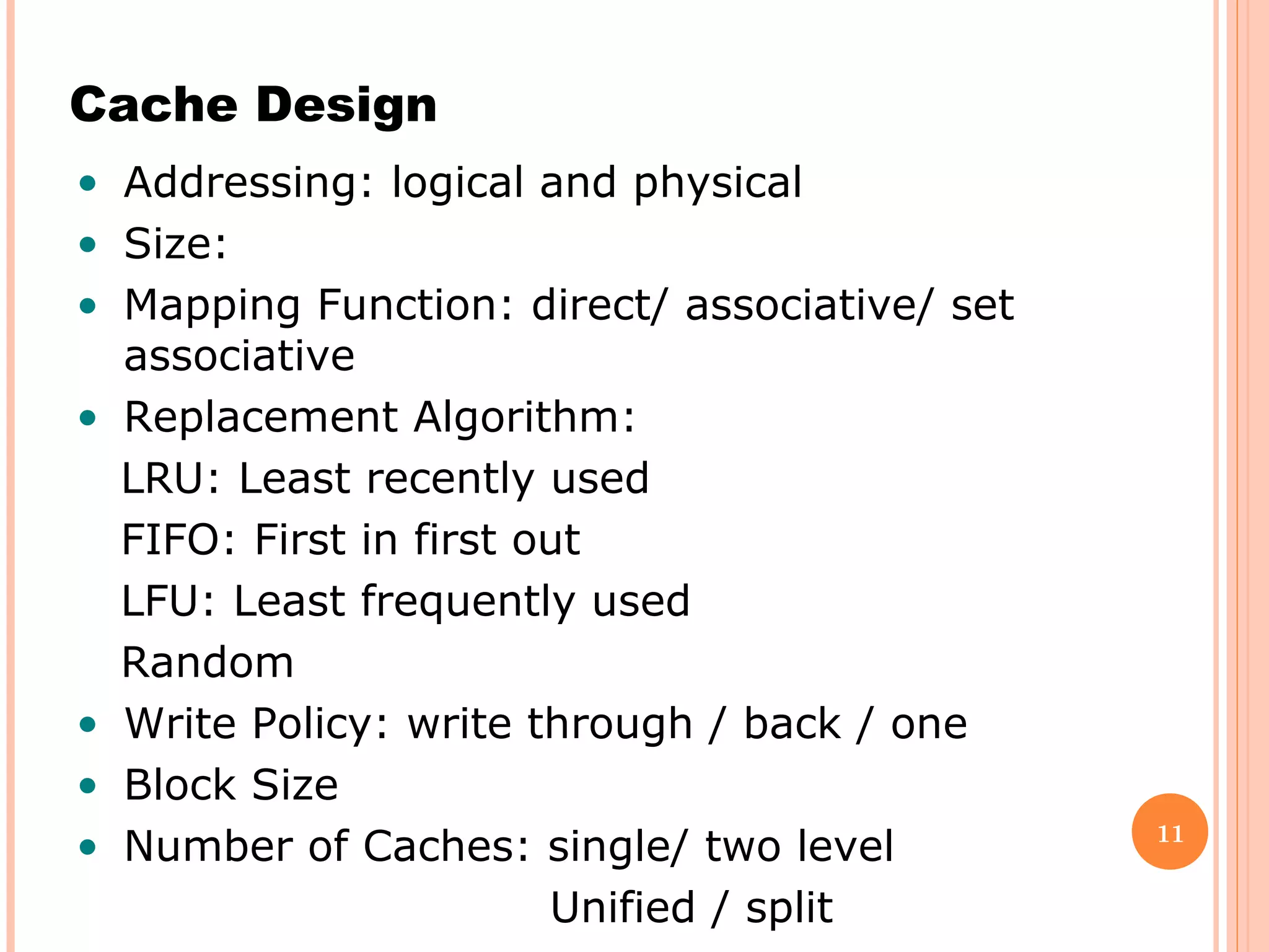
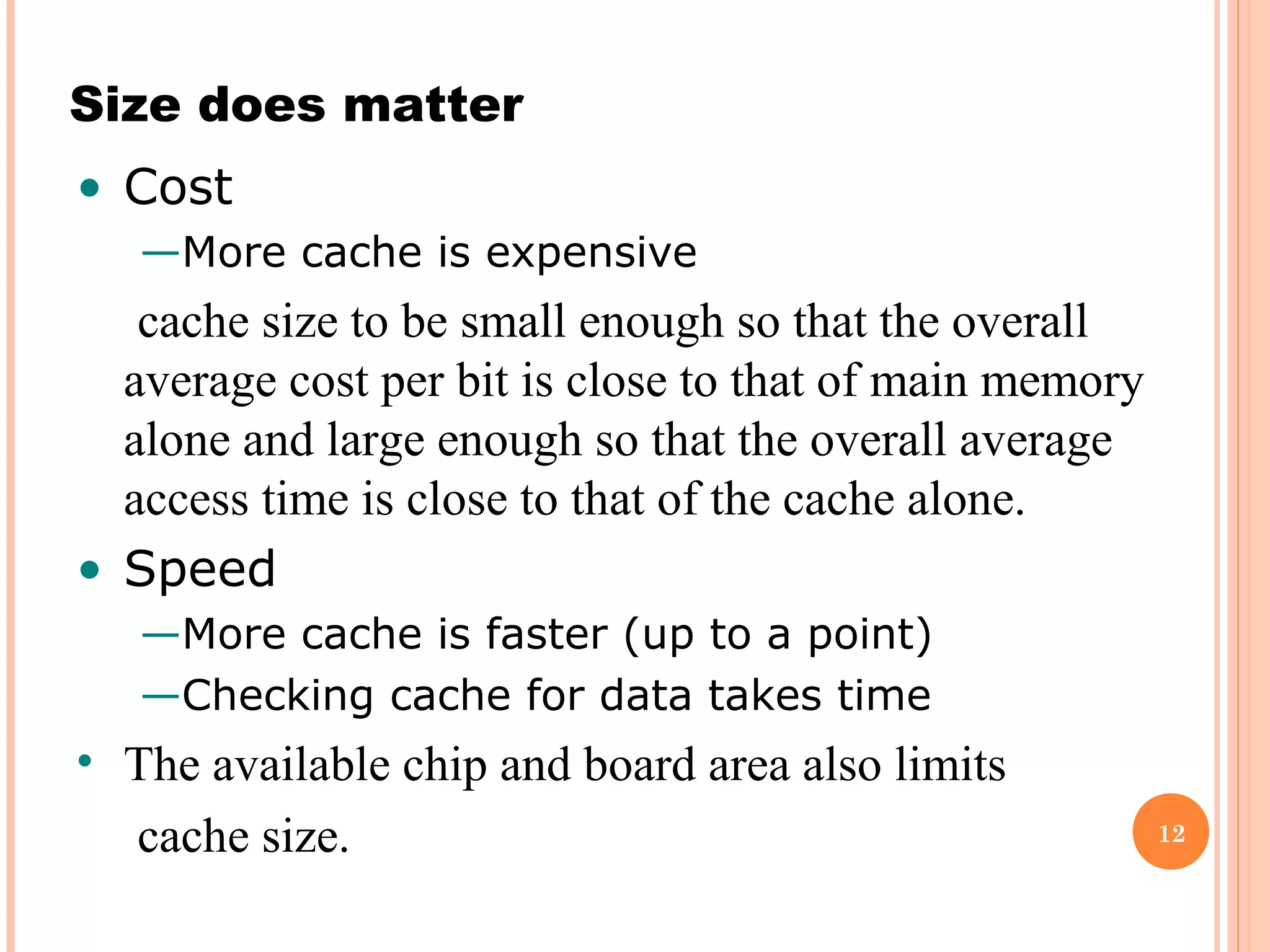
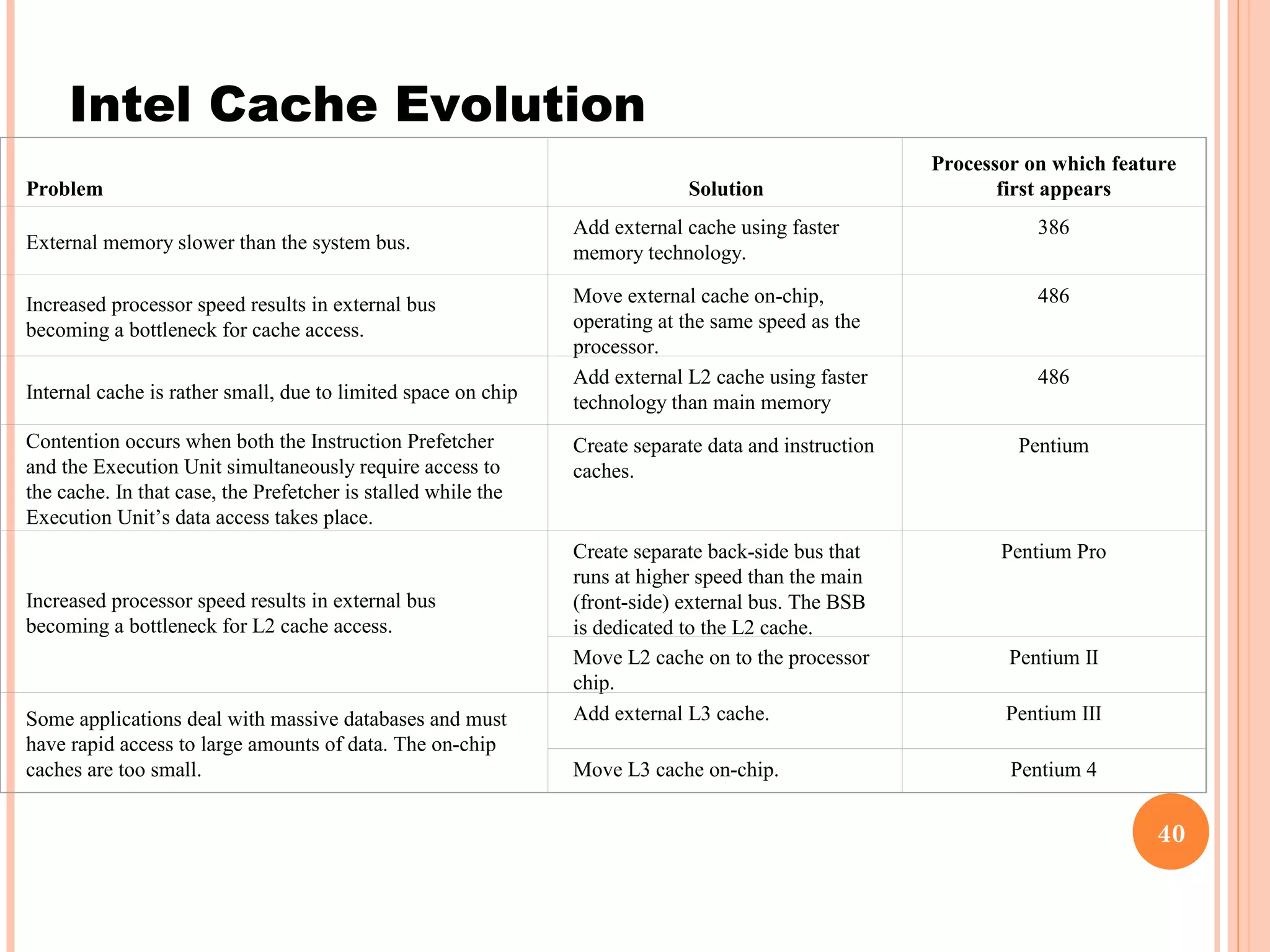
KEMBAR78
Computer architecture cache memory | PPT
CACHE
MEMORY
By :
Nagham
1
What is a Cache Memorey
1. Cache memory is small, high speed RAM buffer
located between CUU and the main memory.
2. Cache memory hold copy of the instructions
(instruction cache) or Data (Operand or Data cache)
currently being used by the CPU.
3. The main purpose od a cache is to accelerate the
computer while keeping the price of the computer low.
2
Cache and Main Memory
3
4
 Processor is much faster than the main memory.
 As a result, the processor has to spend much of its time waiting
while instructions and data are being fetched from the main
memory.
 Major obstacle towards achieving good performance.
 Speed of the main memory cannot be increased beyond a
certain point.
 Cache memory is an architectural arrangement which makes
the main memory appear faster to the processor than it
really is.
 Cache memory is based on the property of computer
programs known as “locality of reference”.
Cache memory
5
 Cache memory is based on the concept of locality of
reference.
 If active segments of a program are placed in a fast cache
memory, then the execution time can be reduced.
 Temporal locality of reference:
 Whenever an instruction or data is needed for the first time, it
should be brought into a cache. It will hopefully be used again
repeatedly.
 Spatial locality of reference:
 Instead of fetching just one item from the main memory to the
cache at a time, several items that have addresses adjacent to
the item being fetched may be useful.
 The term “block” refers to a set of contiguous addresses
locations of some size.
Locality of reference
Levels of Cache: Cache memory is categorized in levels based on it’s closeness
and accessibility to the microprocessor. There are three levels of a cache.
Level 1(L1) Cache: This cache is inbuilt in the processor and is made of SRAM(Static RAM)
Each time the processor requests information from memory, the cache controller on the chip uses
special circuitry to first check if the memory data is already in the cache. If it is present, then the system
is spared from time consuming access to the main memory. In a typical CPU, primary cache ranges in
size from 8 to 64 KB, with larger amounts on the newer processors. This type of Cache Memory is very
fast because it runs at the speed of the processor since it is integrated into it.
Level 2(L2) Cache: The L2 cache is larger but slower in speed than L1 cache. It is used to see
recent accesses that is not picked by L1 cache and is usually 64 to 2 MB in size. A L2 cache is also
found on the CPU. If L1 and L2 cache are used together, then the missing information that is not
present in L1 cache can be retrieved quickly from the L2 cache. Like L1 caches, L2 caches are
composed of SRAM but they are much larger. L2 is usually a separate static RAM (SRAM) chip and it
is placed between the CPU & DRAM(Main Memory)
Level 3(L3) Cache: L3 Cache memory is an enhanced form of memory present on the
motherboard of the computer. It is an extra cache built into the motherboard between the processor and
main memory to speed up the processing operations. It reduces the time gap between request and
retrieving of the data and instructions much more quickly than a main memory. L3 cache are being used
with processors nowadays, having more than 3 MB of storage in it.
6
Diagram showing different types of cache and their
position in the computer system
7
8
Cache/Main Memory Structure
9
Cache operation – overview
• CPU requests contents of memory location
• Check cache for this data
• If present, get from cache (fast)
• If not present, read required block from
main memory to cache
• Then deliver from cache to CPU
• Cache includes tags to identify which
block of main memory is in each cache
slot
10
Cache Read Operation - Flowchart
11
Cache Design
• Addressing: logical and physical
• Size:
• Mapping Function: direct/ associative/ set
associative
• Replacement Algorithm:
LRU: Least recently used
FIFO: First in first out
LFU: Least frequently used
Random
• Write Policy: write through / back / one
• Block Size
• Number of Caches: single/ two level
Unified / split
12
Size does matter
• Cost
—More cache is expensive
cache size to be small enough so that the overall
average cost per bit is close to that of main memory
alone and large enough so that the overall average
access time is close to that of the cache alone.
• Speed
—More cache is faster (up to a point)
—Checking cache for data takes time
• The available chip and board area also limits
cache size.
13
Cache Mapping functions
The address issued by the processor may
correspond to that of an element that exists
currently in the cache (cache hit); otherwise, it
may correspond to an element that is currently
residing in the main memory.
Therefore, address translation has to be made
in order to determine the location of the
requested element. This is one of the functions
performed by the memory management unit
(MMU).
ORGANIZATION
THERE ARE THREE MAIN
DIFFERENT ORGANIZATION
TECHNIQUES USED FOR
CACHE MEMORY. THE THREE
TECHNIQUES ARE :
1. DIRECT MAPPING.
2. FULLY ASSOCIATIVE MAPPING
3. SET-ASSOCIATIVE MAPPING
14
15
Direct mapping
This is the simplest among the three
techniques. Its simplicity stems from the
fact that it places an incoming main memory
block into a specific fixed cache block
location. The placement is done based on a
fixed relation between the incoming block
number, i, the cache block number, j, and
the number of cache blocks, N: j = i mod N
16
Direct mapping : Example 1
Example 1: Consider, for example, the case of a main
memory consisting of 4K blocks, a cache memory
consisting of 128 blocks, and a block size of 16 words.
As the figure shows, there are a total of 32 main memory
blocks that map to
a given cache block. For example, main memory blocks 0,
128, 256, 384, . . . , 3968 map to cache block 0.
ADVANTAGE & DISADVANTAGE
17
The main advantage of the direct-mapping
technique is its simplicity in determining
where to place an incoming main memory
block in the cache.
Its main disadvantage is the inefficient use
of the cache. This is because a number of
main memory blocks may compete for a
given cache block even if there exist other
empty cache blocks. This disadvantage
should lead to achieving a low cache hit
ratio.
18
According to the direct-mapping technique the
MMU interprets the address issued by the
processor by dividing the address into three
fields:
1. Word field = log2 B, where B is the size of
the block in words.
2. Block field = log2 N, where N is the size of
the cache in blocks.
3. Tag field = log2 (M/N), where M is the size of
the main memory in blocks.
4. The number of bits in the main memory
address = log (B x M)
DIRECT MAPPING EXAMPLE 2
19
20
We illustrate the protocol using the parameters given in the example
The steps of the protocol are:
1. Use the Block field to determine the cache block that should contain the
element requested by the processor. The Block field is used directly to determine
the cache block, hence the name of the technique: direct-mapping.
2. Check the corresponding Tag memory to see whether there is a match
between its content and that of the Tag field. A match between the two indicates
that the targeted cache block determined in step 1 is currently holding the main
memory element requested by the processor, that is, a cache hit.
3. Among the elements contained in the cache block, the targeted element can
be selected using the Word field.
4. If in step 2, no match is found, then this indicates a cache miss.
Therefore, the required block has to be brought from the main
memory, deposited in the cache, and the targeted element is made
available to the processor. The cache Tag memory and the cache block
memory have to be updated accordingly.
21
FULLY ASSOCIATIVE MAPPING
22
According to this technique, an incoming main memory block can
be placed in any available cache block. Therefore, the address
issued by the processor need only have two fields. These are the
Tag and Word fields. The first uniquely identifies the block while
residing in the cache. The second field identifies the element
within the block that is requested by the processor.
1. Word field = log2
B, where B is the size of the block in words
2. Tag field = log2
M, where M is the size of the main memory in
blocks
3. The number of bits in the main memory address = log2
(B
x M)
23
Example 3
Compute the above three parameters for a memory system
having the following specification: size of the main memory is
4K blocks, size of the cache is 128 blocks, and the block size
is 16 words. Assume that the system uses associative
mapping:
Word field = log2 B = log2 16 = log2 24
= 4 bits
Tag field = log2 M = log2 27
x 210
= 12 bits
The number of bits in the main memory address = log2 (B x M)
=
log2 (24
x 212
) = 16 bits.
24
The steps of the protocol are:
1. Use the Tag field to search in the Tag memory for a match with any
of the tags stored.
2. A match in the tag memory indicates that the corresponding targeted
cache block determined in step 1 is currently holding the main memory
element requested by the processor, that is, a cache hit.
3. Among the elements contained in the cache block, the targeted
element can be selected using the Word field.
4. If in step 2, no match is found, then this indicates a cache miss.
Therefore, the required block has to be brought from the main memory,
deposited in the first available cache block, and the targeted element
(word) is made available to the processor. The cache Tag memory and
the cache block memory have to be updated accordingly.
25
It should be noted that the search made in step 1 above requires
matching the tag field of the address with each and every entry in the
tag memory. Such a search, if done sequentially, could lead to a long
delay. Therefore, the tags are stored in an associative memory
(content addressable). This allows the entire contents of the tag
memory to be searched in parallel (associatively), hence the name,
associative mapping.
26
FULLY ASSOCIATIVE MAPPING
ADVANTAGES & DISADVANATGES
The main advantage of the associative-mapping
technique is the efficient use of the cache. This stems
from the fact that there exists no restriction on where
to place incoming main memory blocks. Any
unoccupied cache block can potentially be used to
receive those incoming main memory blocks.
The main disadvantage of the technique, is the
hardware overhead required to perform the
associative search conducted in order to find a match
between the tag field and the tag memory as
discussed above.
SET-ASSOCIATIVE MAPPING
27
In the set-associative mapping technique, the cache is
divided into a number of sets. Each set consists of a
number of blocks. A given main memory block maps to a
specific cache set based on the equation s = i mod S,
where S is the number of sets in the cache, i is
the main memory block number, and s is the specific
cache set to which block i maps.
However, an incoming block maps to any block in the
assigned cache set. Therefore, the address issued by the
processor is divided into three distinct fields. These are the
Tag, Set, and Word fields.
28
The length, in bits, of each of the fields of Figure 6.9 is given by:
1. Word field = log2 B, where B is the size of the block in words
2. Set field = log2 S, where S is the number of sets in the cache
3. Tag field = log2 (M/S), where M is the size of the main memory in
blocks.
S = N/Bs, where N is the number of cache blocks and Bs is the number
of
blocks per set
4. The number of bits in the main memory address = log2 (B x M)
EXAMPLE 4
29
Compute the above three parameters (Word, Set, and Tag) for a
memory system having the following specification: size of the main
memory is 4K blocks, size of the cache is 128 blocks, and the block
size is 16 words.
Assume that the system uses set-associative mapping with four blocks
per set.
S = 128/4 = 32 sets:
1. Word field = log2 B = log2 16 = log2 24
= 4 bits
2. Set field = log2 32 = 5 bits
3. Tag field = log2 (4 x 210
/32) = 7 bits
The number of bits in the main memory address = log2 (B x M) = log2
(24
x212
) = 16 bits.
30
31
The steps of the protocol are:
1. Use the Set field (5 bits) to determine (directly) the specified
set (1 of the
32 sets).
 
2. Use the Tag field to find a match with any of the (four) blocks
in the determined set. A match in the tag memory indicates that
the specified set
determined in step 1 is currently holding the targeted block, that
is, a cache hit.
3. Among the 16 words (elements) contained in hit cache block,
the requested word is selected using a selector with the help of
the Word field.
32
4. If in step 2, no match is found, then this indicates a cache
miss. Therefore, the required block has to be brought from the
main memory, deposited in the specified set first, and the
targeted element (word) is made available to the processor. The
cache Tag memory and the cache block memory have to be
updated accordingly.
It should be noted that the search made in step 2 above requires
matching the tag field of the address with each and every entry
in the tag memory for the specified set.
Such a search is performed in parallel (associatively) over the
set, hence the name, set-associative mapping.
33
34
35
36
Hit Ratio
the ratio of the total numbers
of hits divided by the total CPU
accesses to memory (1.e. hits
plus misses) is called hit ratio.
Hit ratio = total numbers of hits / total numbers of
hits + total numbers of miss
37
38
Line Size
• Retrieve not only desired word but a number of
adjacent words as well
• Increased block size will increase hit ratio at first
—the principle of locality
• Hit ratio will decreases as block becomes even
bigger
—Probability of using newly fetched information becomes
less than probability of reusing replaced
• Larger blocks
—Reduce number of blocks that fit in cache
—Data overwritten shortly after being fetched
—Each additional word is less local so less likely to be
needed
• No definitive optimum value has been found
• 8 to 64 bytes seems reasonable
• For HPC systems, 64- and 128-byte most
common
39
Unified v Split Caches
• One cache for data and instructions or
two, one for data and one for instructions
• Advantages of unified cache
—Higher hit rate
– Balances load of instruction and data fetch
– Only one cache to design & implement
• Advantages of split cache
—Eliminates cache contention between
instruction fetch/decode unit and execution
unit
– Important in pipelining
40
Intel Cache Evolution
Problem Solution
Processor on which feature
first appears
External memory slower than the system bus.
Add external cache using faster
memory technology.
386
Increased processor speed results in external bus
becoming a bottleneck for cache access.
Move external cache on-chip,
operating at the same speed as the
processor.
486
Internal cache is rather small, due to limited space on chip
Add external L2 cache using faster
technology than main memory
486
Contention occurs when both the Instruction Prefetcher
and the Execution Unit simultaneously require access to
the cache. In that case, the Prefetcher is stalled while the
Execution Unit’s data access takes place.
Create separate data and instruction
caches.
Pentium
Increased processor speed results in external bus
becoming a bottleneck for L2 cache access.
Create separate back-side bus that
runs at higher speed than the main
(front-side) external bus. The BSB
is dedicated to the L2 cache.
Pentium Pro
Move L2 cache on to the processor
chip.
Pentium II
Some applications deal with massive databases and must
have rapid access to large amounts of data. The on-chip
caches are too small.
Add external L3 cache. Pentium III
Move L3 cache on-chip. Pentium 4
41

Computer architecture cache memory

  • 1.
  • 2.
    What is aCache Memorey 1. Cache memory is small, high speed RAM buffer located between CUU and the main memory. 2. Cache memory hold copy of the instructions (instruction cache) or Data (Operand or Data cache) currently being used by the CPU. 3. The main purpose od a cache is to accelerate the computer while keeping the price of the computer low. 2
  • 3.
  • 4.
    4  Processor ismuch faster than the main memory.  As a result, the processor has to spend much of its time waiting while instructions and data are being fetched from the main memory.  Major obstacle towards achieving good performance.  Speed of the main memory cannot be increased beyond a certain point.  Cache memory is an architectural arrangement which makes the main memory appear faster to the processor than it really is.  Cache memory is based on the property of computer programs known as “locality of reference”. Cache memory
  • 5.
    5  Cache memoryis based on the concept of locality of reference.  If active segments of a program are placed in a fast cache memory, then the execution time can be reduced.  Temporal locality of reference:  Whenever an instruction or data is needed for the first time, it should be brought into a cache. It will hopefully be used again repeatedly.  Spatial locality of reference:  Instead of fetching just one item from the main memory to the cache at a time, several items that have addresses adjacent to the item being fetched may be useful.  The term “block” refers to a set of contiguous addresses locations of some size. Locality of reference
  • 6.
    Levels of Cache:Cache memory is categorized in levels based on it’s closeness and accessibility to the microprocessor. There are three levels of a cache. Level 1(L1) Cache: This cache is inbuilt in the processor and is made of SRAM(Static RAM) Each time the processor requests information from memory, the cache controller on the chip uses special circuitry to first check if the memory data is already in the cache. If it is present, then the system is spared from time consuming access to the main memory. In a typical CPU, primary cache ranges in size from 8 to 64 KB, with larger amounts on the newer processors. This type of Cache Memory is very fast because it runs at the speed of the processor since it is integrated into it. Level 2(L2) Cache: The L2 cache is larger but slower in speed than L1 cache. It is used to see recent accesses that is not picked by L1 cache and is usually 64 to 2 MB in size. A L2 cache is also found on the CPU. If L1 and L2 cache are used together, then the missing information that is not present in L1 cache can be retrieved quickly from the L2 cache. Like L1 caches, L2 caches are composed of SRAM but they are much larger. L2 is usually a separate static RAM (SRAM) chip and it is placed between the CPU & DRAM(Main Memory) Level 3(L3) Cache: L3 Cache memory is an enhanced form of memory present on the motherboard of the computer. It is an extra cache built into the motherboard between the processor and main memory to speed up the processing operations. It reduces the time gap between request and retrieving of the data and instructions much more quickly than a main memory. L3 cache are being used with processors nowadays, having more than 3 MB of storage in it. 6
  • 7.
    Diagram showing differenttypes of cache and their position in the computer system 7
  • 8.
  • 9.
    9 Cache operation –overview • CPU requests contents of memory location • Check cache for this data • If present, get from cache (fast) • If not present, read required block from main memory to cache • Then deliver from cache to CPU • Cache includes tags to identify which block of main memory is in each cache slot
  • 10.
  • 11.
    11 Cache Design • Addressing:logical and physical • Size: • Mapping Function: direct/ associative/ set associative • Replacement Algorithm: LRU: Least recently used FIFO: First in first out LFU: Least frequently used Random • Write Policy: write through / back / one • Block Size • Number of Caches: single/ two level Unified / split
  • 12.
    12 Size does matter •Cost —More cache is expensive cache size to be small enough so that the overall average cost per bit is close to that of main memory alone and large enough so that the overall average access time is close to that of the cache alone. • Speed —More cache is faster (up to a point) —Checking cache for data takes time • The available chip and board area also limits cache size.
  • 13.
    13 Cache Mapping functions Theaddress issued by the processor may correspond to that of an element that exists currently in the cache (cache hit); otherwise, it may correspond to an element that is currently residing in the main memory. Therefore, address translation has to be made in order to determine the location of the requested element. This is one of the functions performed by the memory management unit (MMU).
  • 14.
    ORGANIZATION THERE ARE THREEMAIN DIFFERENT ORGANIZATION TECHNIQUES USED FOR CACHE MEMORY. THE THREE TECHNIQUES ARE : 1. DIRECT MAPPING. 2. FULLY ASSOCIATIVE MAPPING 3. SET-ASSOCIATIVE MAPPING 14
  • 15.
    15 Direct mapping This isthe simplest among the three techniques. Its simplicity stems from the fact that it places an incoming main memory block into a specific fixed cache block location. The placement is done based on a fixed relation between the incoming block number, i, the cache block number, j, and the number of cache blocks, N: j = i mod N
  • 16.
    16 Direct mapping :Example 1 Example 1: Consider, for example, the case of a main memory consisting of 4K blocks, a cache memory consisting of 128 blocks, and a block size of 16 words. As the figure shows, there are a total of 32 main memory blocks that map to a given cache block. For example, main memory blocks 0, 128, 256, 384, . . . , 3968 map to cache block 0.
  • 17.
    ADVANTAGE & DISADVANTAGE 17 Themain advantage of the direct-mapping technique is its simplicity in determining where to place an incoming main memory block in the cache. Its main disadvantage is the inefficient use of the cache. This is because a number of main memory blocks may compete for a given cache block even if there exist other empty cache blocks. This disadvantage should lead to achieving a low cache hit ratio.
  • 18.
    18 According to thedirect-mapping technique the MMU interprets the address issued by the processor by dividing the address into three fields: 1. Word field = log2 B, where B is the size of the block in words. 2. Block field = log2 N, where N is the size of the cache in blocks. 3. Tag field = log2 (M/N), where M is the size of the main memory in blocks. 4. The number of bits in the main memory address = log (B x M)
  • 19.
  • 20.
    20 We illustrate theprotocol using the parameters given in the example The steps of the protocol are: 1. Use the Block field to determine the cache block that should contain the element requested by the processor. The Block field is used directly to determine the cache block, hence the name of the technique: direct-mapping. 2. Check the corresponding Tag memory to see whether there is a match between its content and that of the Tag field. A match between the two indicates that the targeted cache block determined in step 1 is currently holding the main memory element requested by the processor, that is, a cache hit. 3. Among the elements contained in the cache block, the targeted element can be selected using the Word field. 4. If in step 2, no match is found, then this indicates a cache miss. Therefore, the required block has to be brought from the main memory, deposited in the cache, and the targeted element is made available to the processor. The cache Tag memory and the cache block memory have to be updated accordingly.
  • 21.
  • 22.
    FULLY ASSOCIATIVE MAPPING 22 Accordingto this technique, an incoming main memory block can be placed in any available cache block. Therefore, the address issued by the processor need only have two fields. These are the Tag and Word fields. The first uniquely identifies the block while residing in the cache. The second field identifies the element within the block that is requested by the processor. 1. Word field = log2 B, where B is the size of the block in words 2. Tag field = log2 M, where M is the size of the main memory in blocks 3. The number of bits in the main memory address = log2 (B x M)
  • 23.
    23 Example 3 Compute theabove three parameters for a memory system having the following specification: size of the main memory is 4K blocks, size of the cache is 128 blocks, and the block size is 16 words. Assume that the system uses associative mapping: Word field = log2 B = log2 16 = log2 24 = 4 bits Tag field = log2 M = log2 27 x 210 = 12 bits The number of bits in the main memory address = log2 (B x M) = log2 (24 x 212 ) = 16 bits.
  • 24.
    24 The steps ofthe protocol are: 1. Use the Tag field to search in the Tag memory for a match with any of the tags stored. 2. A match in the tag memory indicates that the corresponding targeted cache block determined in step 1 is currently holding the main memory element requested by the processor, that is, a cache hit. 3. Among the elements contained in the cache block, the targeted element can be selected using the Word field. 4. If in step 2, no match is found, then this indicates a cache miss. Therefore, the required block has to be brought from the main memory, deposited in the first available cache block, and the targeted element (word) is made available to the processor. The cache Tag memory and the cache block memory have to be updated accordingly.
  • 25.
    25 It should benoted that the search made in step 1 above requires matching the tag field of the address with each and every entry in the tag memory. Such a search, if done sequentially, could lead to a long delay. Therefore, the tags are stored in an associative memory (content addressable). This allows the entire contents of the tag memory to be searched in parallel (associatively), hence the name, associative mapping.
  • 26.
    26 FULLY ASSOCIATIVE MAPPING ADVANTAGES& DISADVANATGES The main advantage of the associative-mapping technique is the efficient use of the cache. This stems from the fact that there exists no restriction on where to place incoming main memory blocks. Any unoccupied cache block can potentially be used to receive those incoming main memory blocks. The main disadvantage of the technique, is the hardware overhead required to perform the associative search conducted in order to find a match between the tag field and the tag memory as discussed above.
  • 27.
    SET-ASSOCIATIVE MAPPING 27 In theset-associative mapping technique, the cache is divided into a number of sets. Each set consists of a number of blocks. A given main memory block maps to a specific cache set based on the equation s = i mod S, where S is the number of sets in the cache, i is the main memory block number, and s is the specific cache set to which block i maps. However, an incoming block maps to any block in the assigned cache set. Therefore, the address issued by the processor is divided into three distinct fields. These are the Tag, Set, and Word fields.
  • 28.
    28 The length, inbits, of each of the fields of Figure 6.9 is given by: 1. Word field = log2 B, where B is the size of the block in words 2. Set field = log2 S, where S is the number of sets in the cache 3. Tag field = log2 (M/S), where M is the size of the main memory in blocks. S = N/Bs, where N is the number of cache blocks and Bs is the number of blocks per set 4. The number of bits in the main memory address = log2 (B x M)
  • 29.
    EXAMPLE 4 29 Compute theabove three parameters (Word, Set, and Tag) for a memory system having the following specification: size of the main memory is 4K blocks, size of the cache is 128 blocks, and the block size is 16 words. Assume that the system uses set-associative mapping with four blocks per set. S = 128/4 = 32 sets: 1. Word field = log2 B = log2 16 = log2 24 = 4 bits 2. Set field = log2 32 = 5 bits 3. Tag field = log2 (4 x 210 /32) = 7 bits The number of bits in the main memory address = log2 (B x M) = log2 (24 x212 ) = 16 bits.
  • 30.
  • 31.
    31 The steps ofthe protocol are: 1. Use the Set field (5 bits) to determine (directly) the specified set (1 of the 32 sets).   2. Use the Tag field to find a match with any of the (four) blocks in the determined set. A match in the tag memory indicates that the specified set determined in step 1 is currently holding the targeted block, that is, a cache hit. 3. Among the 16 words (elements) contained in hit cache block, the requested word is selected using a selector with the help of the Word field.
  • 32.
    32 4. If instep 2, no match is found, then this indicates a cache miss. Therefore, the required block has to be brought from the main memory, deposited in the specified set first, and the targeted element (word) is made available to the processor. The cache Tag memory and the cache block memory have to be updated accordingly. It should be noted that the search made in step 2 above requires matching the tag field of the address with each and every entry in the tag memory for the specified set. Such a search is performed in parallel (associatively) over the set, hence the name, set-associative mapping.
  • 33.
  • 34.
  • 35.
  • 36.
  • 37.
    Hit Ratio the ratioof the total numbers of hits divided by the total CPU accesses to memory (1.e. hits plus misses) is called hit ratio. Hit ratio = total numbers of hits / total numbers of hits + total numbers of miss 37
  • 38.
    38 Line Size • Retrievenot only desired word but a number of adjacent words as well • Increased block size will increase hit ratio at first —the principle of locality • Hit ratio will decreases as block becomes even bigger —Probability of using newly fetched information becomes less than probability of reusing replaced • Larger blocks —Reduce number of blocks that fit in cache —Data overwritten shortly after being fetched —Each additional word is less local so less likely to be needed • No definitive optimum value has been found • 8 to 64 bytes seems reasonable • For HPC systems, 64- and 128-byte most common
  • 39.
    39 Unified v SplitCaches • One cache for data and instructions or two, one for data and one for instructions • Advantages of unified cache —Higher hit rate – Balances load of instruction and data fetch – Only one cache to design & implement • Advantages of split cache —Eliminates cache contention between instruction fetch/decode unit and execution unit – Important in pipelining
  • 40.
    40 Intel Cache Evolution ProblemSolution Processor on which feature first appears External memory slower than the system bus. Add external cache using faster memory technology. 386 Increased processor speed results in external bus becoming a bottleneck for cache access. Move external cache on-chip, operating at the same speed as the processor. 486 Internal cache is rather small, due to limited space on chip Add external L2 cache using faster technology than main memory 486 Contention occurs when both the Instruction Prefetcher and the Execution Unit simultaneously require access to the cache. In that case, the Prefetcher is stalled while the Execution Unit’s data access takes place. Create separate data and instruction caches. Pentium Increased processor speed results in external bus becoming a bottleneck for L2 cache access. Create separate back-side bus that runs at higher speed than the main (front-side) external bus. The BSB is dedicated to the L2 cache. Pentium Pro Move L2 cache on to the processor chip. Pentium II Some applications deal with massive databases and must have rapid access to large amounts of data. The on-chip caches are too small. Add external L3 cache. Pentium III Move L3 cache on-chip. Pentium 4
  • 41.