Overview
Primary functionof a processor(CPU), is to execute
sequences of instructions stored in a memory.
The execution of an instruction in a processor can be
split up into two major phases.
Instruction Fetch(Fetch cycle)
Instruction Execution(Execution cycle)
3.
Fundamental Concepts
Processorfetches one instruction at a time and perform
the operation specified.
Instructions are fetched from successive memory
locations until a branch or a jump instruction is
encountered.
Processor keeps track of the address of the memory
location containing the next instruction to be fetched
using Program Counter (PC).
Instruction Register (IR)
4.
Executing an Instruction
Fetch the contents of the memory location pointed to by
the PC. The contents of this location are loaded into the
IR (fetch phase).
IR ← [[PC]]
Assuming that the memory is byte addressable,
increment the contents of the PC by 4 (fetch phase).
PC ← [PC] + 4
Carry out the actions specified by the instruction in the
IR (execution phase).
Internal organization ofthe
processor
ALU
Registers for temporary storage
Various digital circuits for executing different micro
operations.(gates, MUX, decoders, counters).
Internal path for movement of data between ALU and
registers.
Driver circuits for transmitting signals to external units.
Receiver circuits for incoming signals from external units.
7.
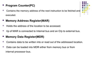
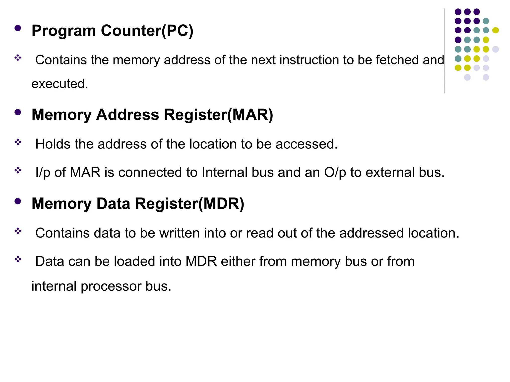
Program Counter(PC)
Contains the memory address of the next instruction to be fetched and
executed.
Memory Address Register(MAR)
Holds the address of the location to be accessed.
I/p of MAR is connected to Internal bus and an O/p to external bus.
Memory Data Register(MDR)
Contains data to be written into or read out of the addressed location.
Data can be loaded into MDR either from memory bus or from
internal processor bus.
8.
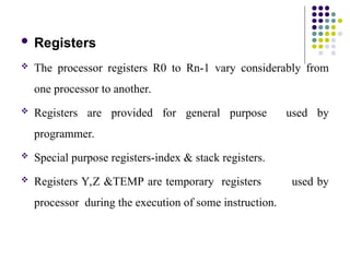
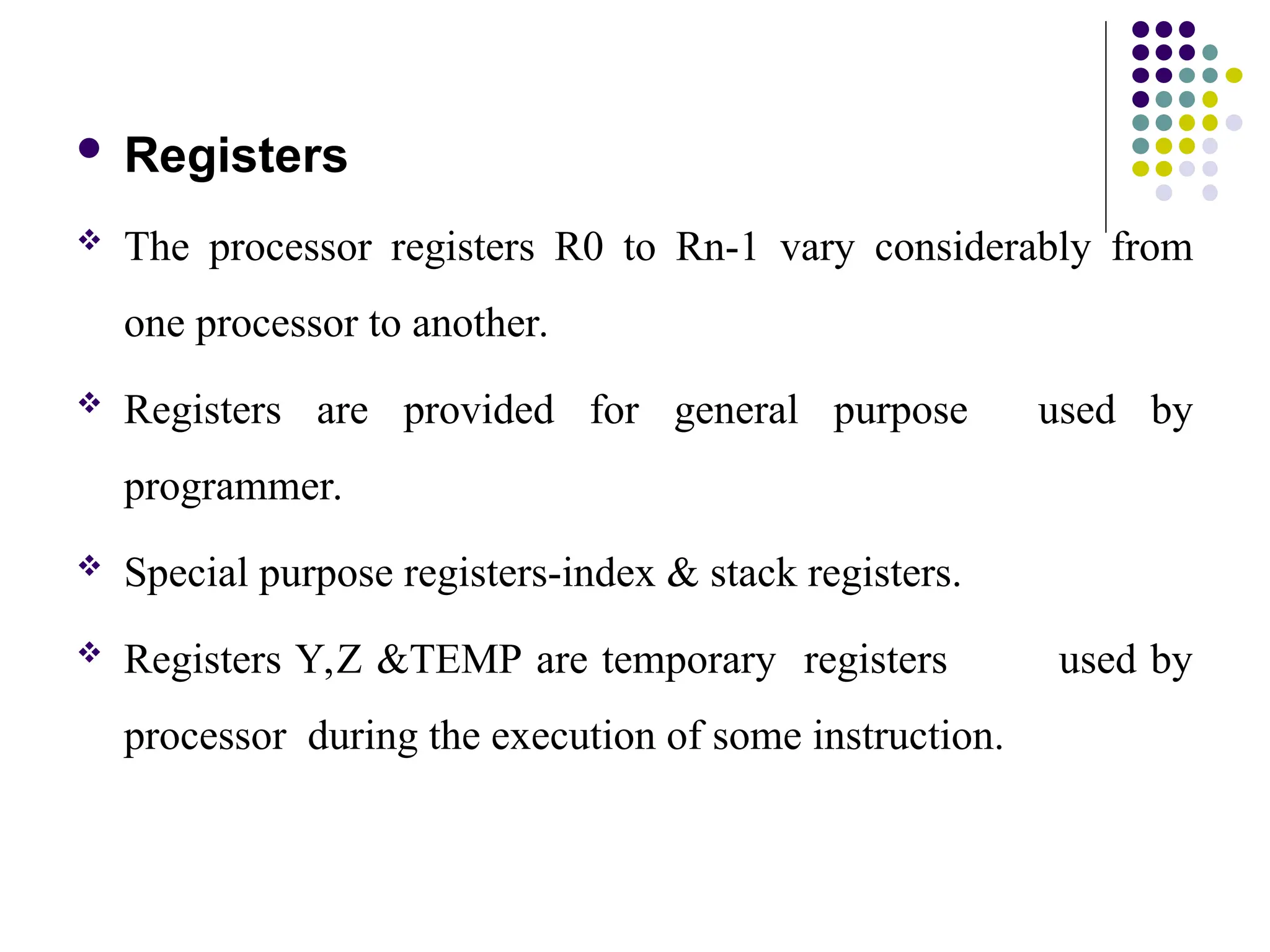
Registers
Theprocessor registers R0 to Rn-1 vary considerably from
one processor to another.
Registers are provided for general purpose used by
programmer.
Special purpose registers-index & stack registers.
Registers Y,Z &TEMP are temporary registers used by
processor during the execution of some instruction.
9.
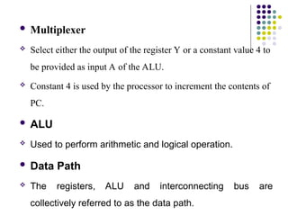
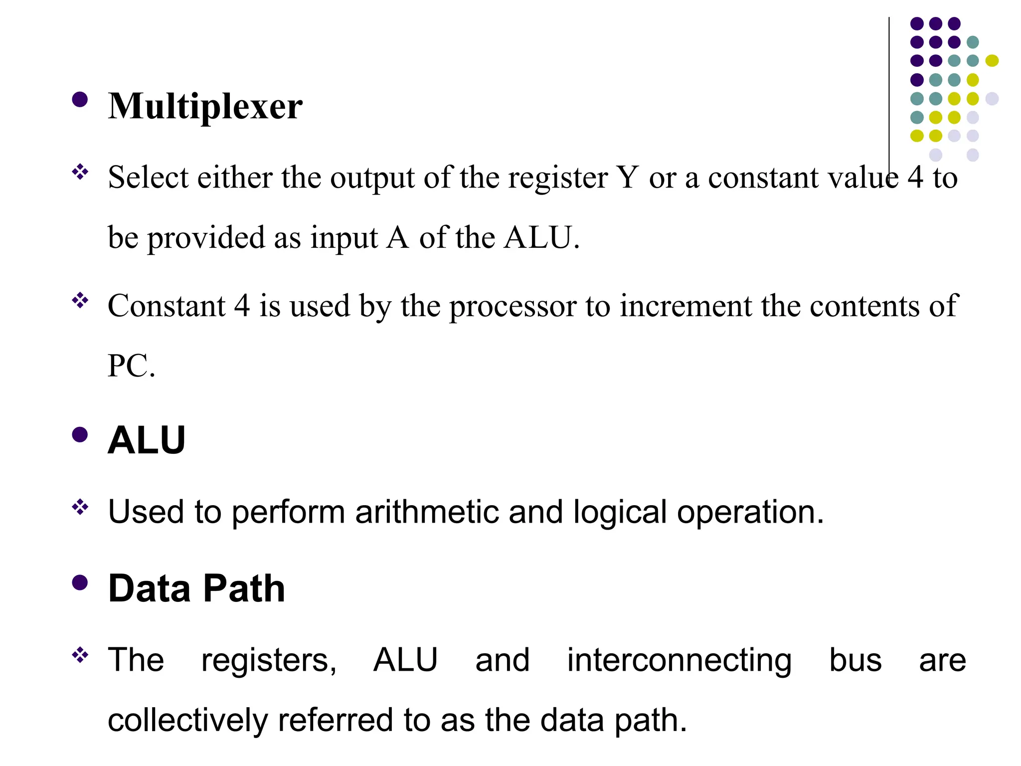
Multiplexer
Selecteither the output of the register Y or a constant value 4 to
be provided as input A of the ALU.
Constant 4 is used by the processor to increment the contents of
PC.
ALU
Used to perform arithmetic and logical operation.
Data Path
The registers, ALU and interconnecting bus are
collectively referred to as the data path.
10.
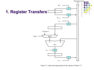
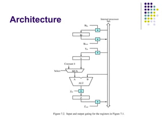
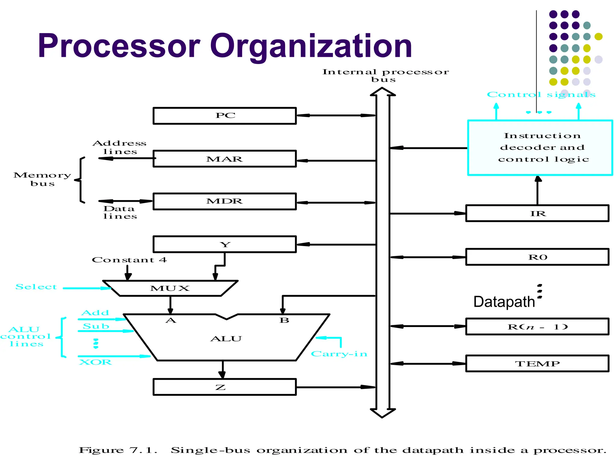
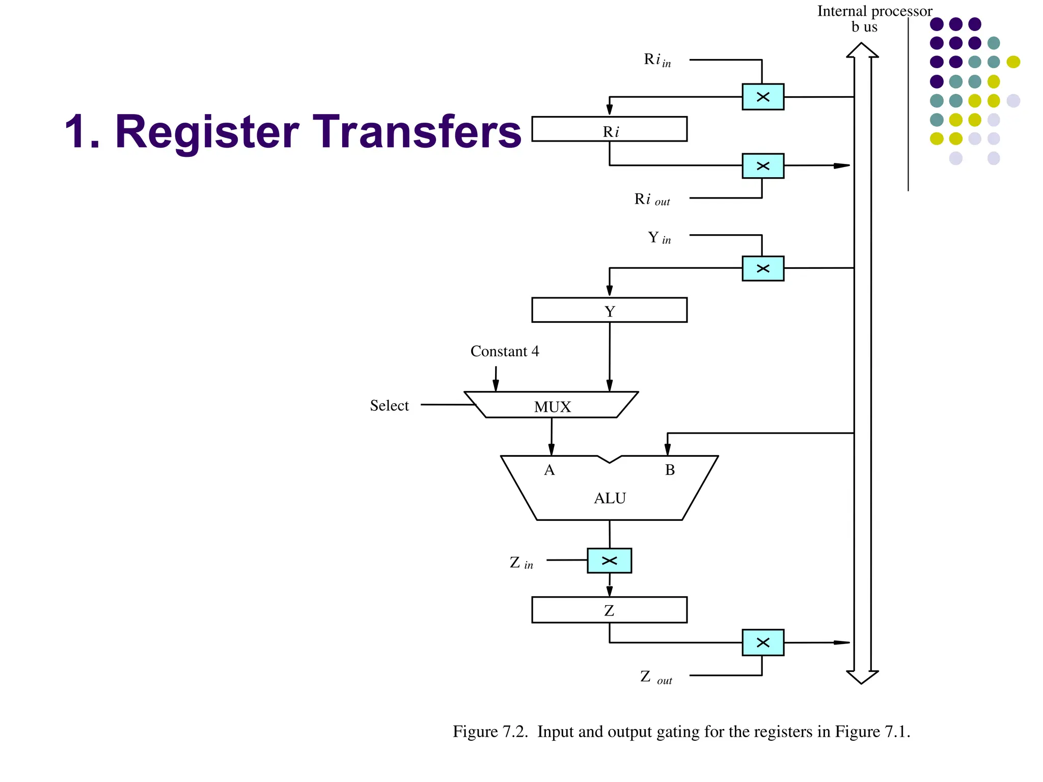
1. Register Transfers
B
A
Z
ALU
Yin
Y
Z in
Z out
Riin
Ri
Ri out
b us
Internal processor
Constant 4
MUX
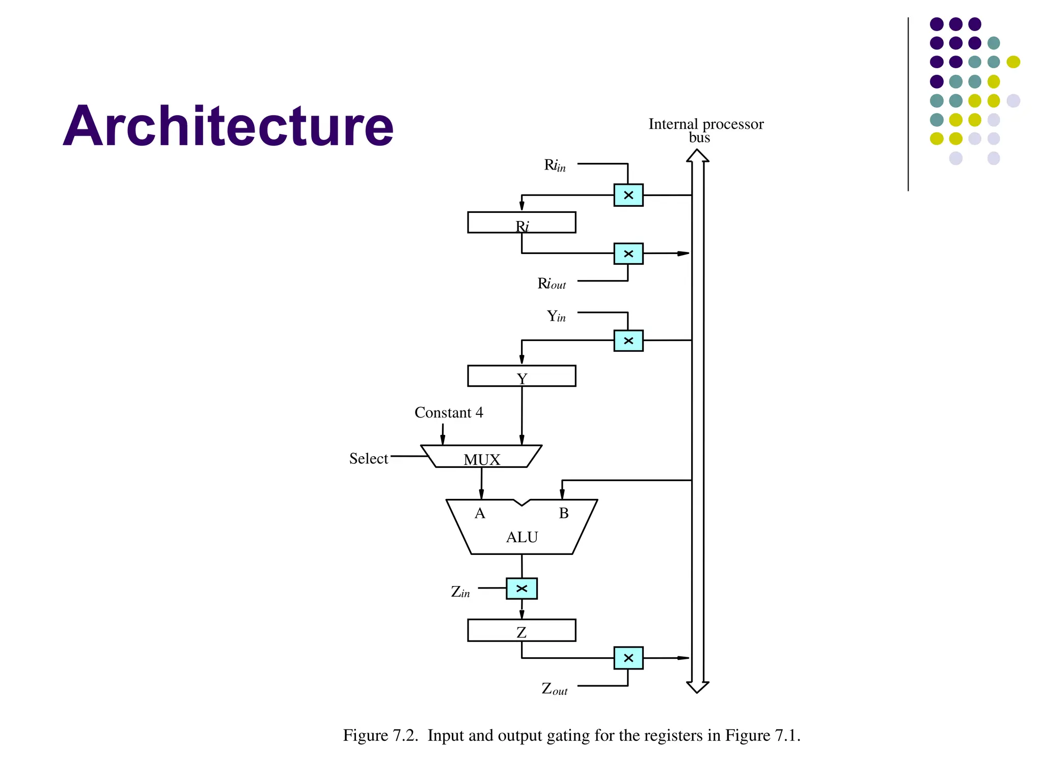
Figure 7.2. Input and output gating for the registers in Figure 7.1.
Select
11.
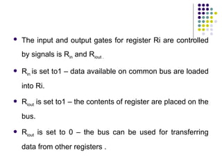
The inputand output gates for register Ri are controlled
by signals is Rin and Riout .
Rin is set to1 – data available on common bus are loaded
into Ri.
Riout is set to1 – the contents of register are placed on the
bus.
Riout is set to 0 – the bus can be used for transferring
data from other registers .
12.
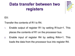
Data transfer betweentwo
registers
EX:
Transfer the contents of R1 to R4.
1. Enable output of register R1 by setting R1out=1. This
places the contents of R1 on the processor bus.
2. Enable input of register R4 by setting R4in=1. This
loads the data from the processor bus into register R4.
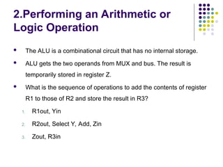
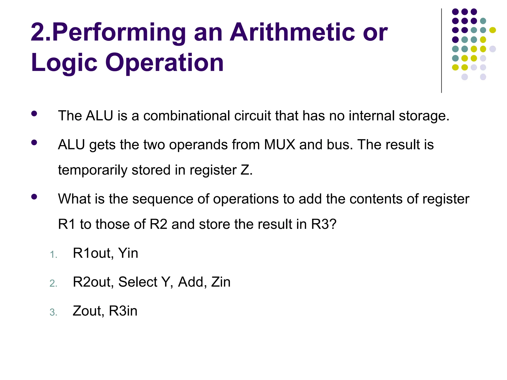
2.Performing an Arithmeticor
Logic Operation
The ALU is a combinational circuit that has no internal storage.
ALU gets the two operands from MUX and bus. The result is
temporarily stored in register Z.
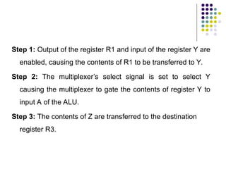
What is the sequence of operations to add the contents of register
R1 to those of R2 and store the result in R3?
1. R1out, Yin
2. R2out, Select Y, Add, Zin
3. Zout, R3in
15.
Step 1: Outputof the register R1 and input of the register Y are
enabled, causing the contents of R1 to be transferred to Y.
Step 2: The multiplexer’s select signal is set to select Y
causing the multiplexer to gate the contents of register Y to
input A of the ALU.
Step 3: The contents of Z are transferred to the destination
register R3.
16.
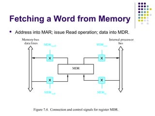
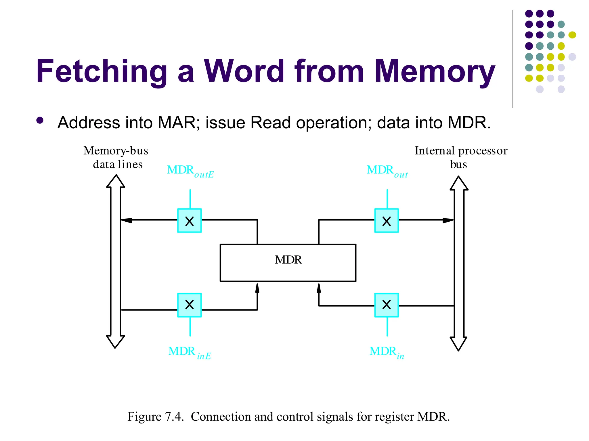
Fetching a Wordfrom Memory
Address into MAR; issue Read operation; data into MDR.
MDR
Memory-bus
Figure 7.4. Connection and control signals for register MDR.
data lines
Internal processor
bus
MDRout
MDRoutE
MDRin
MDRinE
Figure 7.4. Connection and control signals for register MDR.
17.
3.Fetching a Wordfrom Memory
The response time of each memory access varies (cache miss,
memory-mapped I/O,…).
To accommodate this, the processor waits until it receives an
indication that the requested operation has been completed
(Memory-Function-Completed, MFC).
Move (R1), R2
MAR ← [R1]
Start a Read operation on the memory bus
Wait for the MFC response from the memory
Load MDR from the memory bus
R2 ← [MDR]
18.
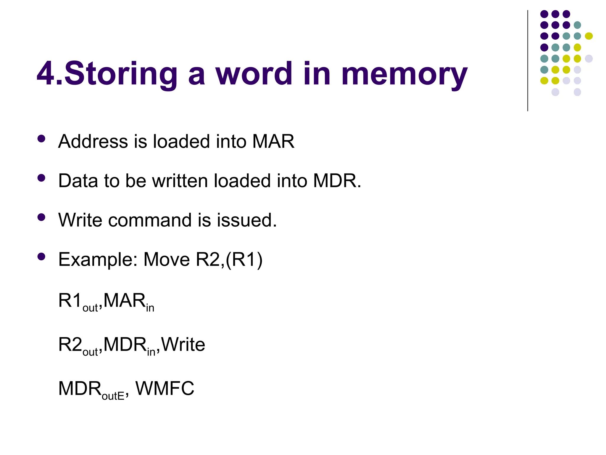
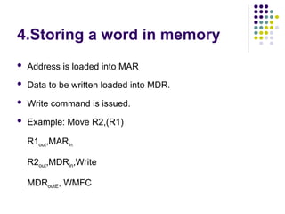
4.Storing a wordin memory
Address is loaded into MAR
Data to be written loaded into MDR.
Write command is issued.
Example: Move R2,(R1)
R1out,MARin
R2out,MDRin,Write
MDRoutE, WMFC
19.
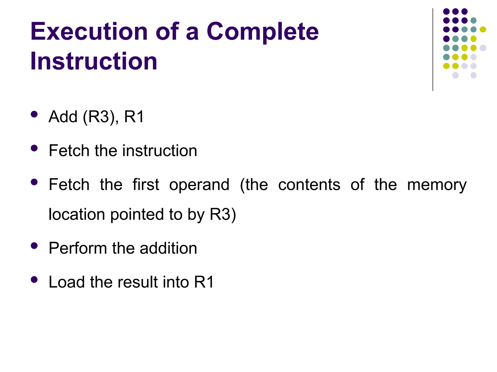
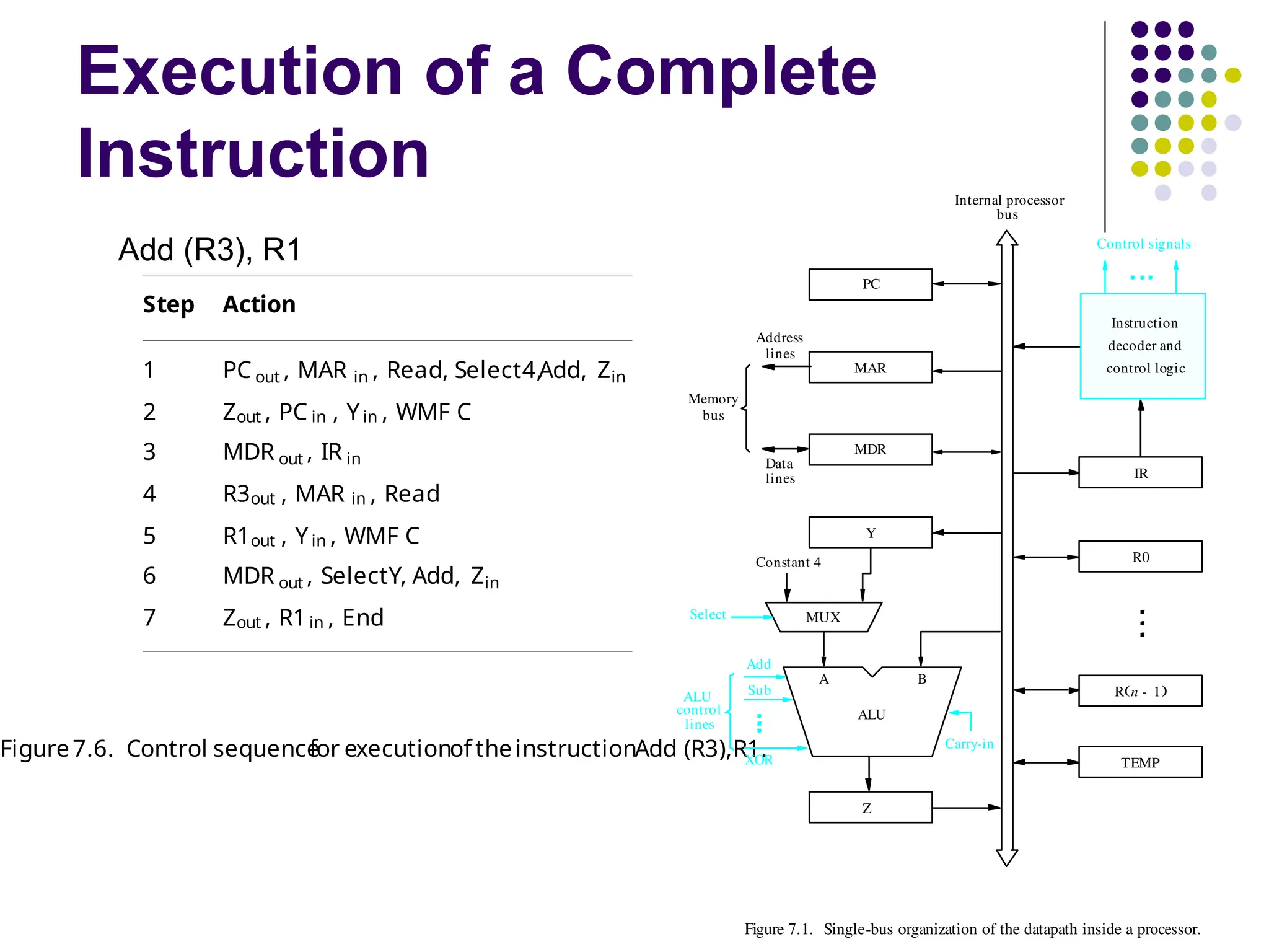
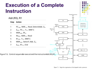
Execution of aComplete
Instruction
Add (R3), R1
Fetch the instruction
Fetch the first operand (the contents of the memory
location pointed to by R3)
Perform the addition
Load the result into R1
20.
Execution of aComplete
Instruction
Step Action
1 PC out , MAR in , Read, Select4,Add, Zin
2 Zout , PC in , Yin , WMF C
3 MDR out , IR in
4 R3out , MAR in , Read
5 R1out , Yin , WMF C
6 MDR out , SelectY, Add, Zin
7 Zout , R1in , End
Figure7.6. Control sequence
for executionof theinstructionAdd (R3),R1.
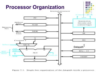
lines
Data
Address
lines
bus
Memory
Carry-in
ALU
PC
MAR
MDR
Y
Z
Add
XOR
Sub
bus
IR
TEMP
R0
control
ALU
lines
Control signals
R n 1
-
Instruction
decoder and
Internal processor
control logic
A B
Figure 7.1. Single-bus organization of the datapath inside a processor.
MUX
Select
Constant 4
Add (R3), R1
21.
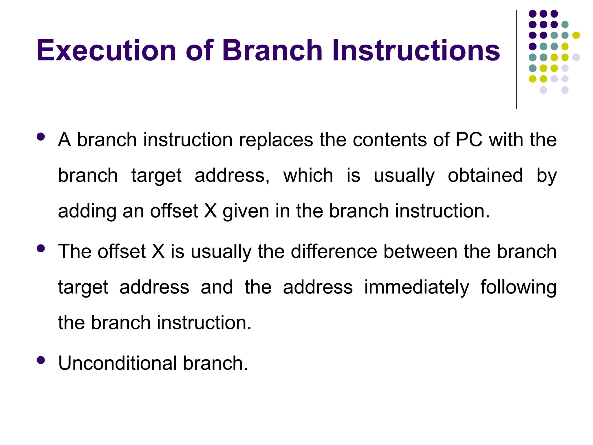
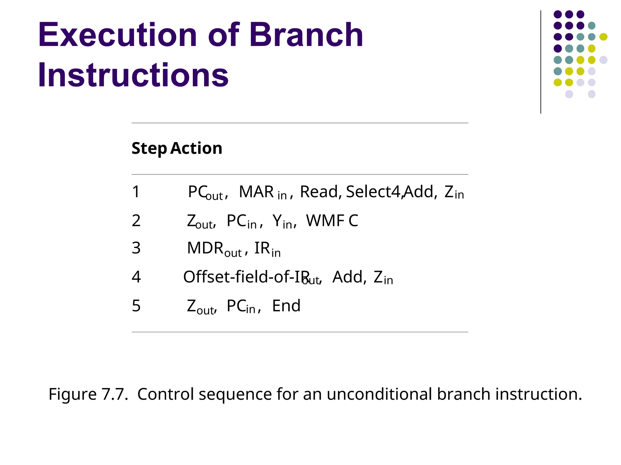
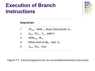
Execution of BranchInstructions
A branch instruction replaces the contents of PC with the
branch target address, which is usually obtained by
adding an offset X given in the branch instruction.
The offset X is usually the difference between the branch
target address and the address immediately following
the branch instruction.
Unconditional branch.
22.
Execution of Branch
Instructions
StepAction
1 PCout, MAR in , Read, Select4,Add, Zin
2 Zout, PCin , Yin, WMF C
3 MDRout , IRin
4 Offset-field-of-IR
out, Add, Zin
5 Zout, PCin , End
Figure 7.7. Control sequence for an unconditional branch instruction.
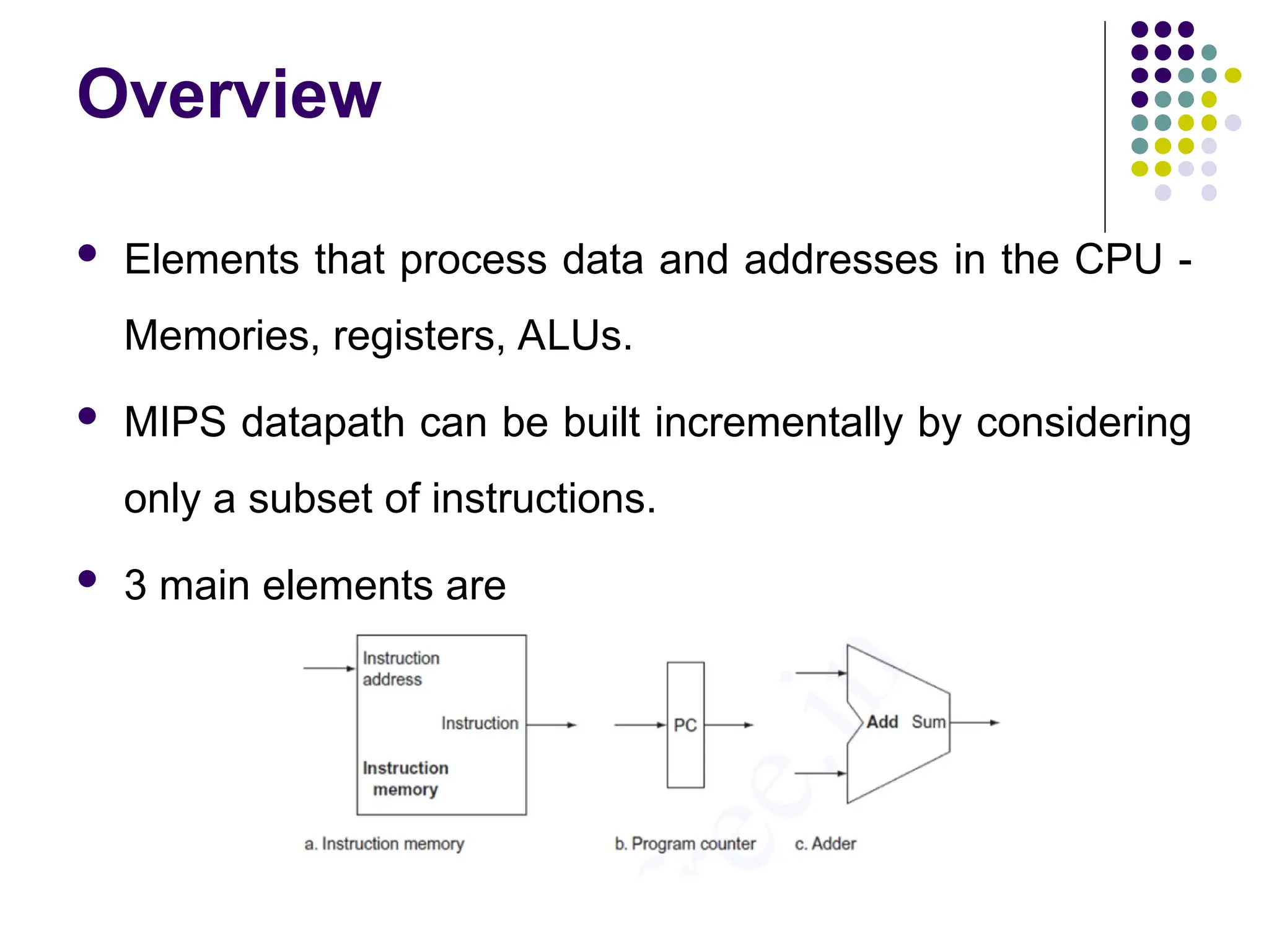
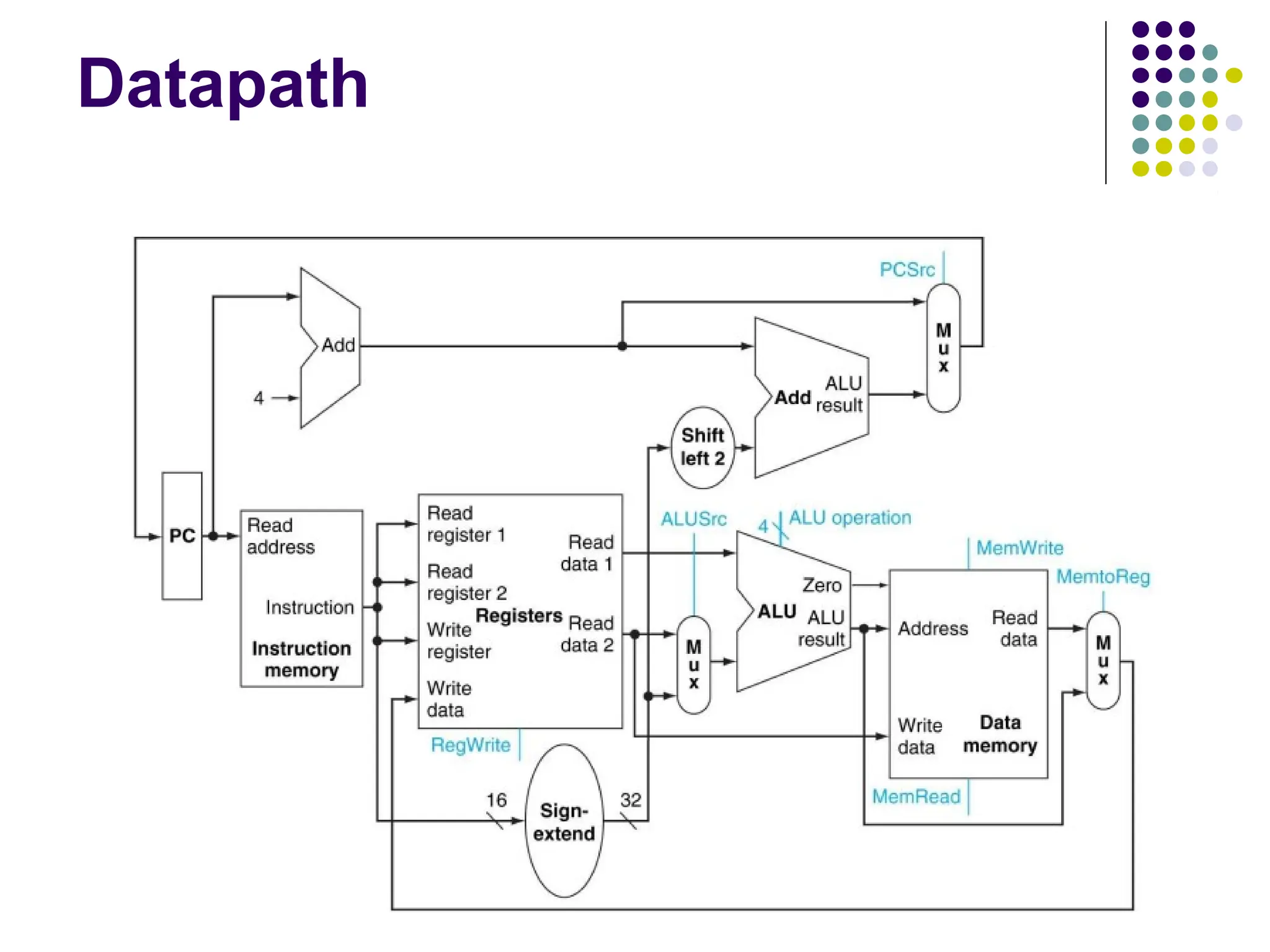
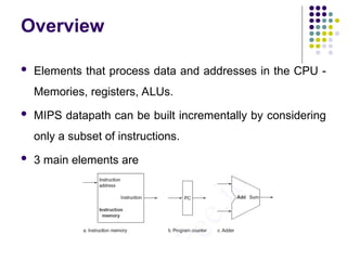
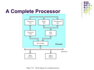
Overview
Elements thatprocess data and addresses in the CPU -
Memories, registers, ALUs.
MIPS datapath can be built incrementally by considering
only a subset of instructions.
3 main elements are
25.
Three types ofMIPS instructions and see what
the datapath look
Arithmetic and Logical Instructions:
These instructions, such as add and subtract, require the ALU
and register file.
Data Transfer Instructions:
These instructions (like load and store) require access to
memory for reading and writing data.
Branch Instructions:
These instructions (like beq) use the Program Counter (PC),
adder for calculating the target address, and the ALU to evaluate
conditions.
26.
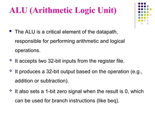
ALU (Arithmetic LogicUnit)
The ALU is a critical element of the datapath,
responsible for performing arithmetic and logical
operations.
It accepts two 32-bit inputs from the register file.
It produces a 32-bit output based on the operation (e.g.,
addition or subtraction).
It also sets a 1-bit zero signal when the result is 0, which
can be used for branch instructions (like beq).
27.
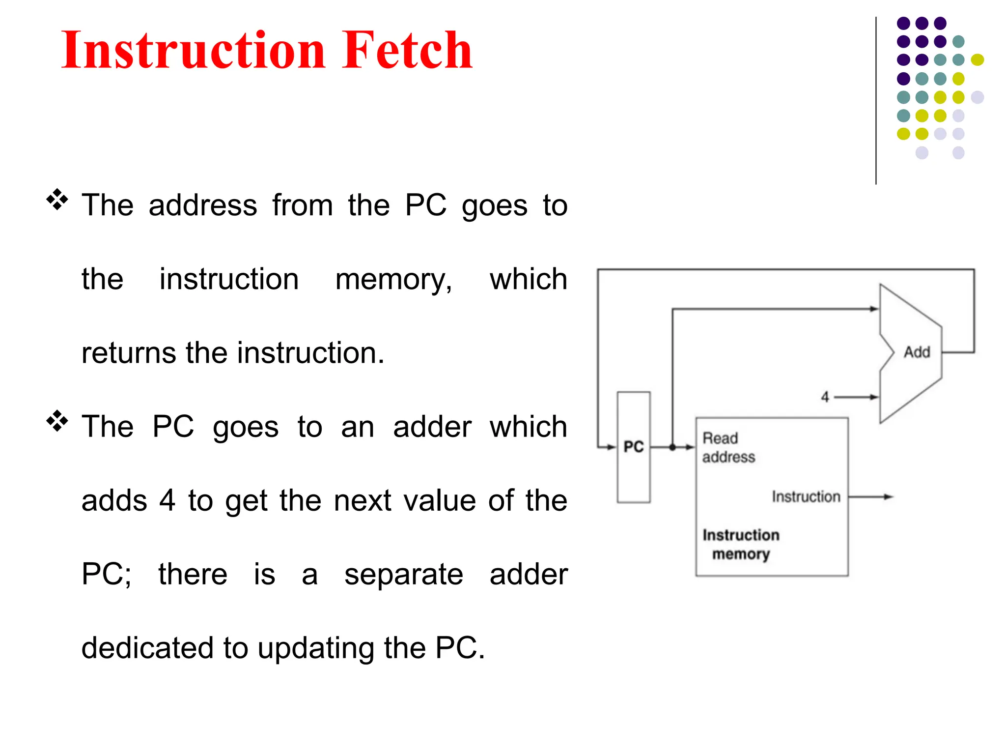
Instruction Fetch
Theaddress from the PC goes to
the instruction memory, which
returns the instruction.
The PC goes to an adder which
adds 4 to get the next value of the
PC; there is a separate adder
dedicated to updating the PC.
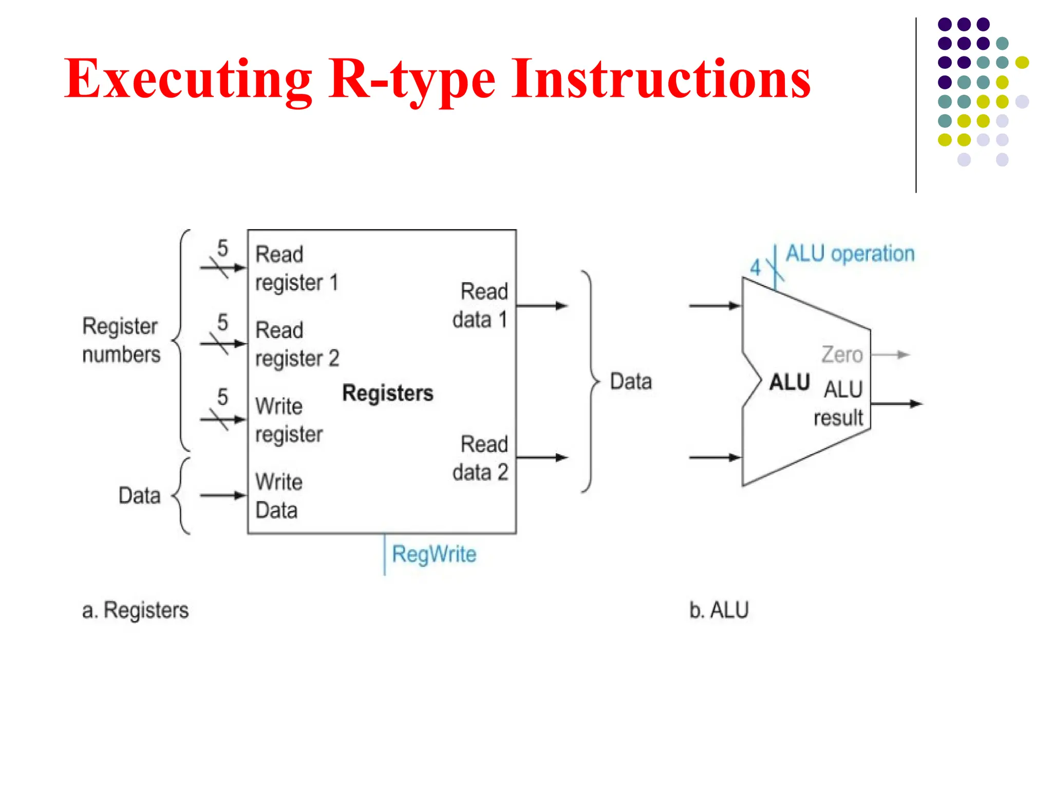
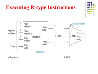
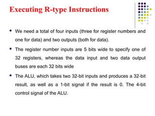
Executing R-type Instructions
We need a total of four inputs (three for register numbers and
one for data) and two outputs (both for data).
The register number inputs are 5 bits wide to specify one of
32 registers, whereas the data input and two data output
buses are each 32 bits wide
The ALU, which takes two 32 bit inputs and produces a 32 bit
‑ ‑
result, as well as a 1-bit signal if the result is 0. The 4-bit
control signal of the ALU.
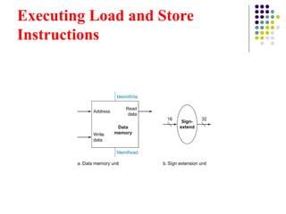
Executing Load andStore
Instructions
The sign extension unit is used to convert a 16-bit
constant into a 32-bit constant.
Example:
In the instruction addi $R1, $R2, 20, the constant 20 is a
16-bit value.
The sign extension unit converts this 16-bit value into a
32-bit value so that it can be processed by the ALU.
ALU Input: The 32-bit extended constant is then passed to
the ALU as one of the inputs for arithmetic operations.
32.
BRANCH INSTRUCTIONS
Theshift left operation is often used in branch instructions to
convert a word address (which is generally represented in 4-
byte increments in MIPS architecture) into a byte address.
Example:
Instruction: BEQ $t0, $t1, 250
Here, 250 represents the offset in words for the branch target.
To calculate the actual byte address, you perform a left shift
by 2:
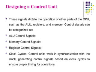
Designing a ControlUnit
These signals dictate the operation of other parts of the CPU,
such as the ALU, registers, and memory. Control signals can
be categorized as:
ALU Control Signals:
Memory Control Signals:
Register Control Signals:
Clock Cycles: Control units work in synchronization with the
clock, generating control signals based on clock cycles to
ensure proper timing for operations.
35.
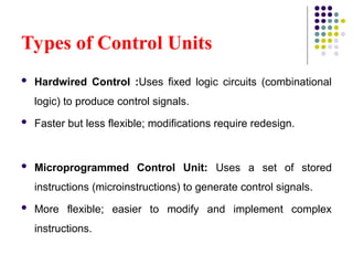
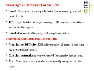
Types of ControlUnits
Hardwired Control :Uses fixed logic circuits (combinational
logic) to produce control signals.
Faster but less flexible; modifications require redesign.
Microprogrammed Control Unit: Uses a set of stored
instructions (microinstructions) to generate control signals.
More flexible; easier to modify and implement complex
instructions.
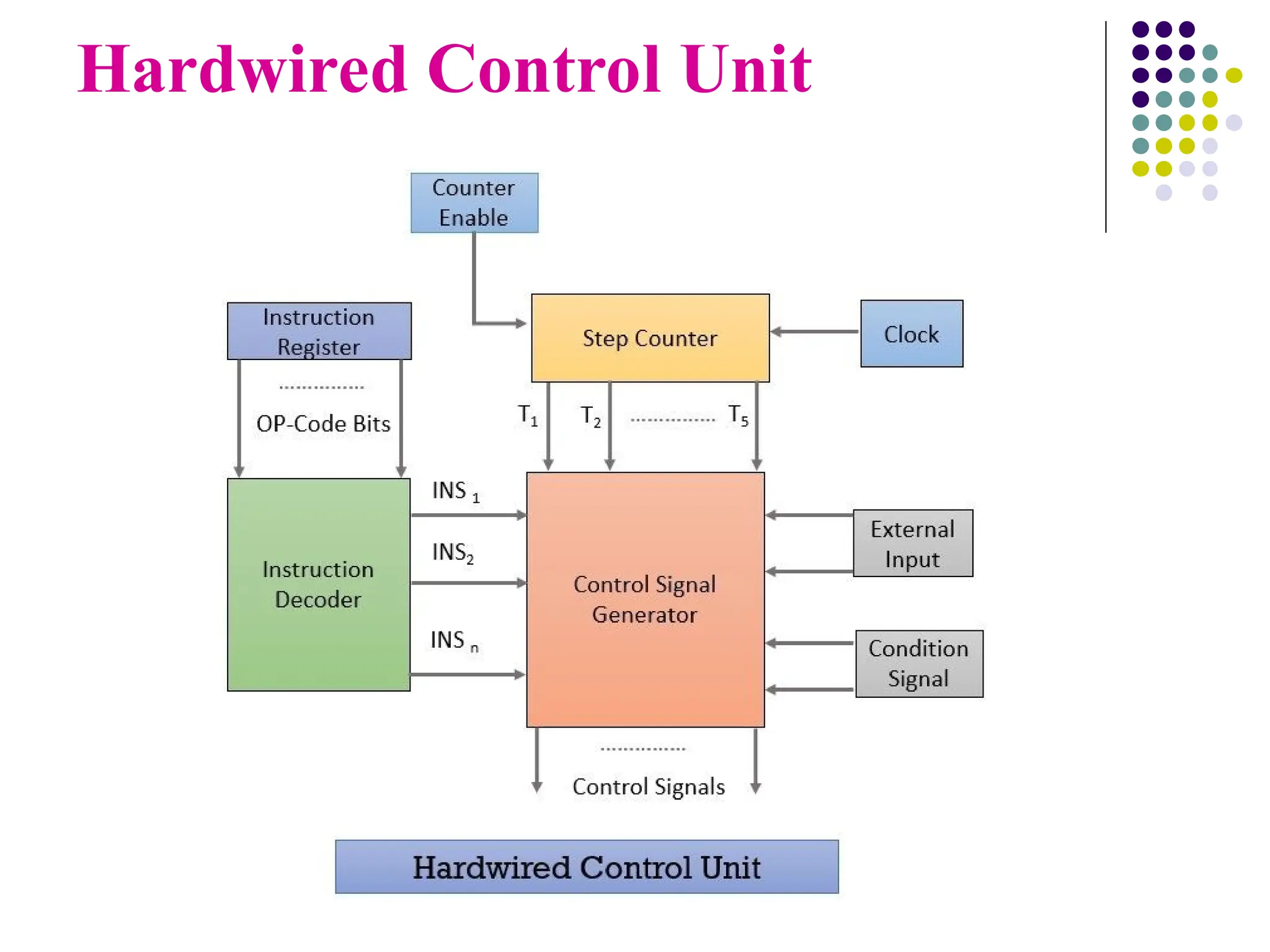
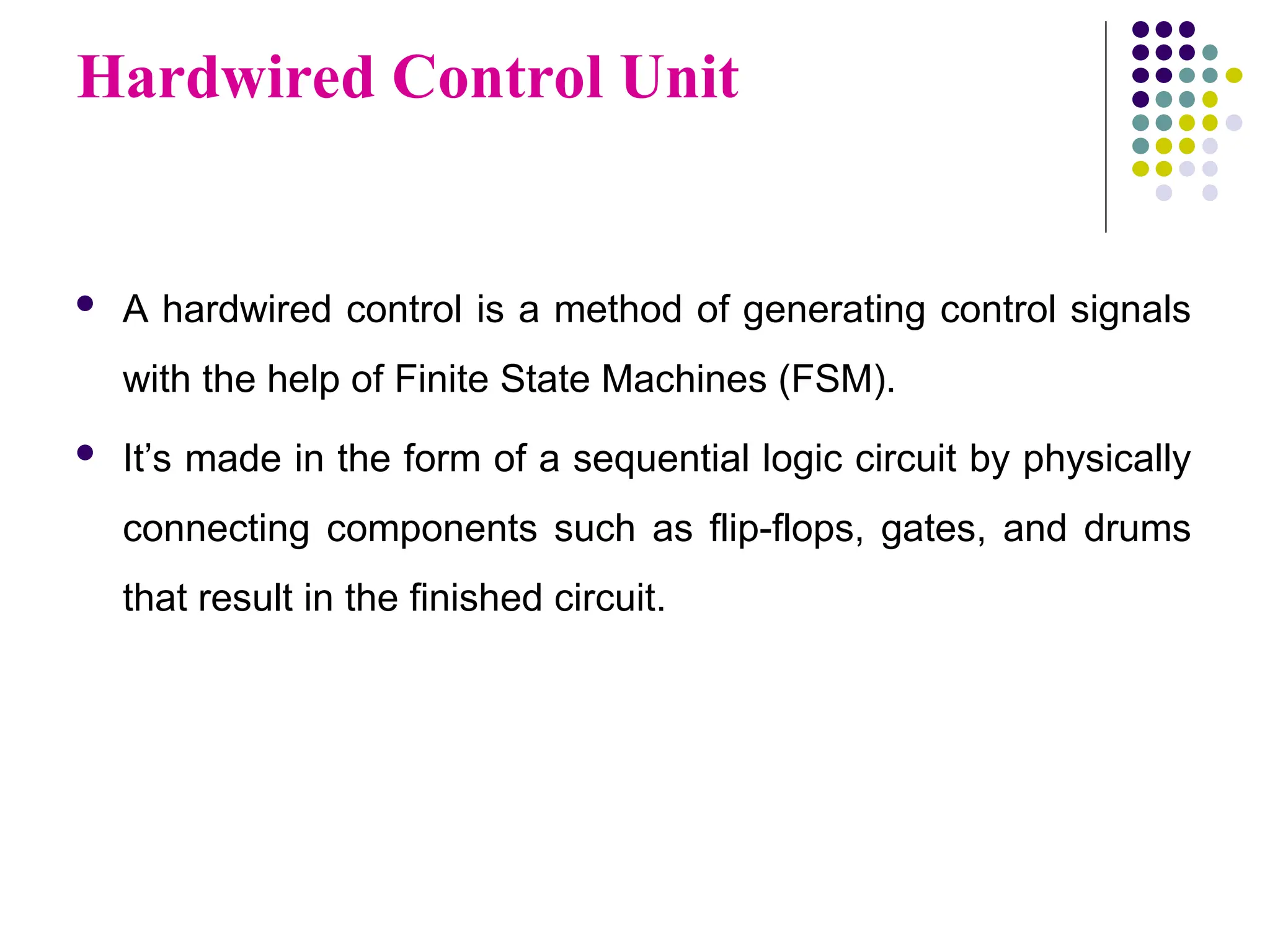
Hardwired Control Unit
A hardwired control is a method of generating control signals
with the help of Finite State Machines (FSM).
It’s made in the form of a sequential logic circuit by physically
connecting components such as flip-flops, gates, and drums
that result in the finished circuit.
38.
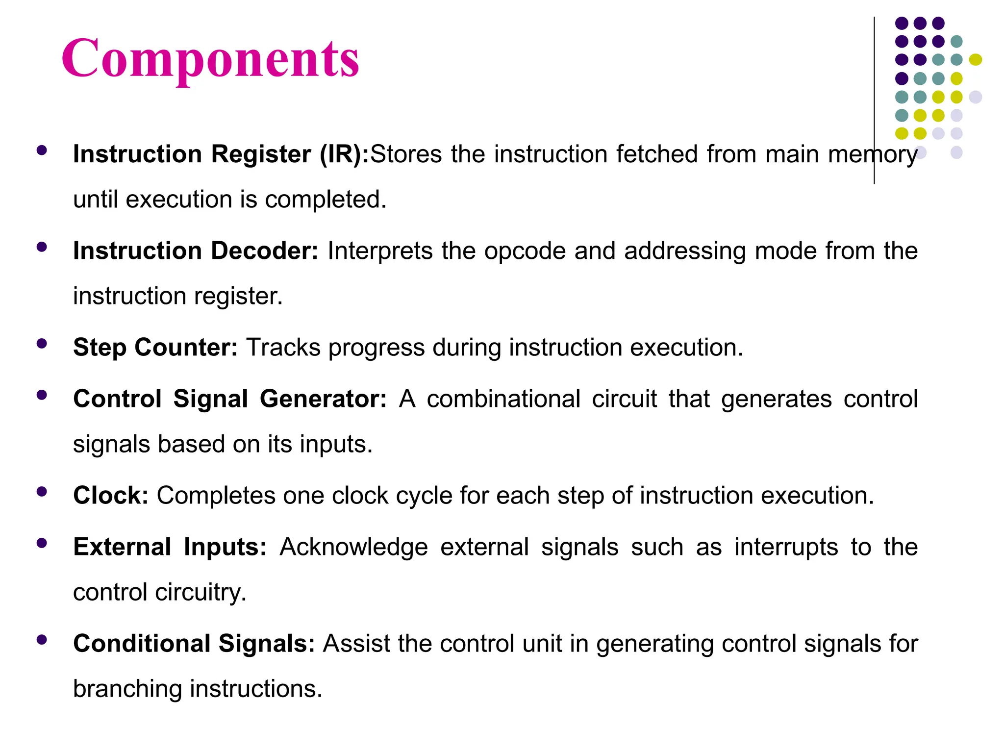
Components
Instruction Register(IR):Stores the instruction fetched from main memory
until execution is completed.
Instruction Decoder: Interprets the opcode and addressing mode from the
instruction register.
Step Counter: Tracks progress during instruction execution.
Control Signal Generator: A combinational circuit that generates control
signals based on its inputs.
Clock: Completes one clock cycle for each step of instruction execution.
External Inputs: Acknowledge external signals such as interrupts to the
control circuitry.
Conditional Signals: Assist the control unit in generating control signals for
branching instructions.
39.
Control Signal GenerationProcess
The instruction to be executed is fetched from the main
memory and placed in the instruction register.
The instruction register generates the opcode, which is
interpreted by the instruction decoder.
The instruction decoder activates the corresponding INSi
signal to the control circuitry based on the decoded opcode
bits.
40.
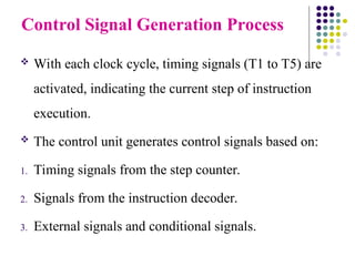
Control Signal GenerationProcess
With each clock cycle, timing signals (T1 to T5) are
activated, indicating the current step of instruction
execution.
The control unit generates control signals based on:
1. Timing signals from the step counter.
2. Signals from the instruction decoder.
3. External signals and conditional signals.
Advantages of HardwiredControl Units
Speed: Generates control signals faster than micro programmed
control units.
Efficiency: Suitable for implementing RISC processors, which are
known for their speed.
Simplicity: Works effectively with simple instructions.
Disadvantages of Hardwired Control Units
Modification Difficulty: Difficult to modify; changes in hardware
require significant effort.
Complex Instructions: Not well-suited for complex instructions.
Cost: More expensive to implement or modify compared to other
types.
43.
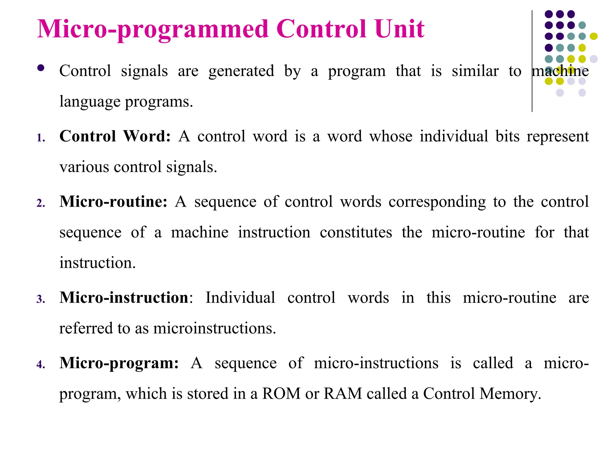
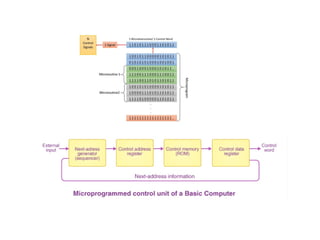
Micro-programmed Control Unit
Control signals are generated by a program that is similar to machine
language programs.
1. Control Word: A control word is a word whose individual bits represent
various control signals.
2. Micro-routine: A sequence of control words corresponding to the control
sequence of a machine instruction constitutes the micro-routine for that
instruction.
3. Micro-instruction: Individual control words in this micro-routine are
referred to as microinstructions.
4. Micro-program: A sequence of micro-instructions is called a micro-
program, which is stored in a ROM or RAM called a Control Memory.
45.
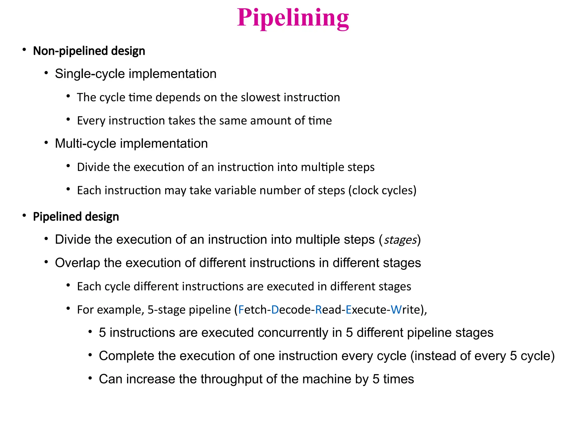
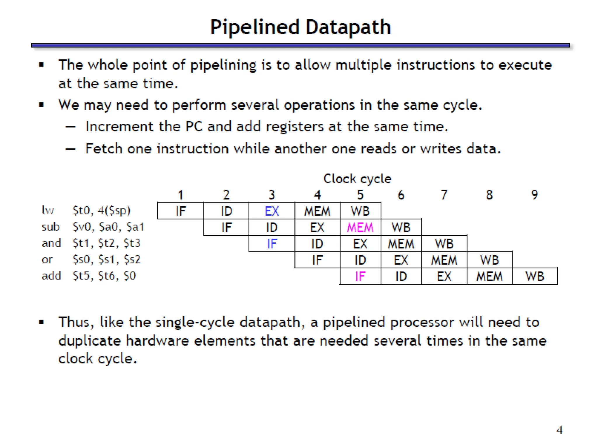
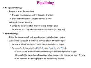
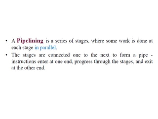
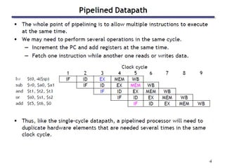
Pipelining
• Non-pipelined design
•Single-cycle implementation
• The cycle time depends on the slowest instruction
• Every instruction takes the same amount of time
• Multi-cycle implementation
• Divide the execution of an instruction into multiple steps
• Each instruction may take variable number of steps (clock cycles)
• Pipelined design
• Divide the execution of an instruction into multiple steps (stages)
• Overlap the execution of different instructions in different stages
• Each cycle different instructions are executed in different stages
• For example, 5-stage pipeline (Fetch-Decode-Read-Execute-Write),
• 5 instructions are executed concurrently in 5 different pipeline stages
• Complete the execution of one instruction every cycle (instead of every 5 cycle)
• Can increase the throughput of the machine by 5 times
48.
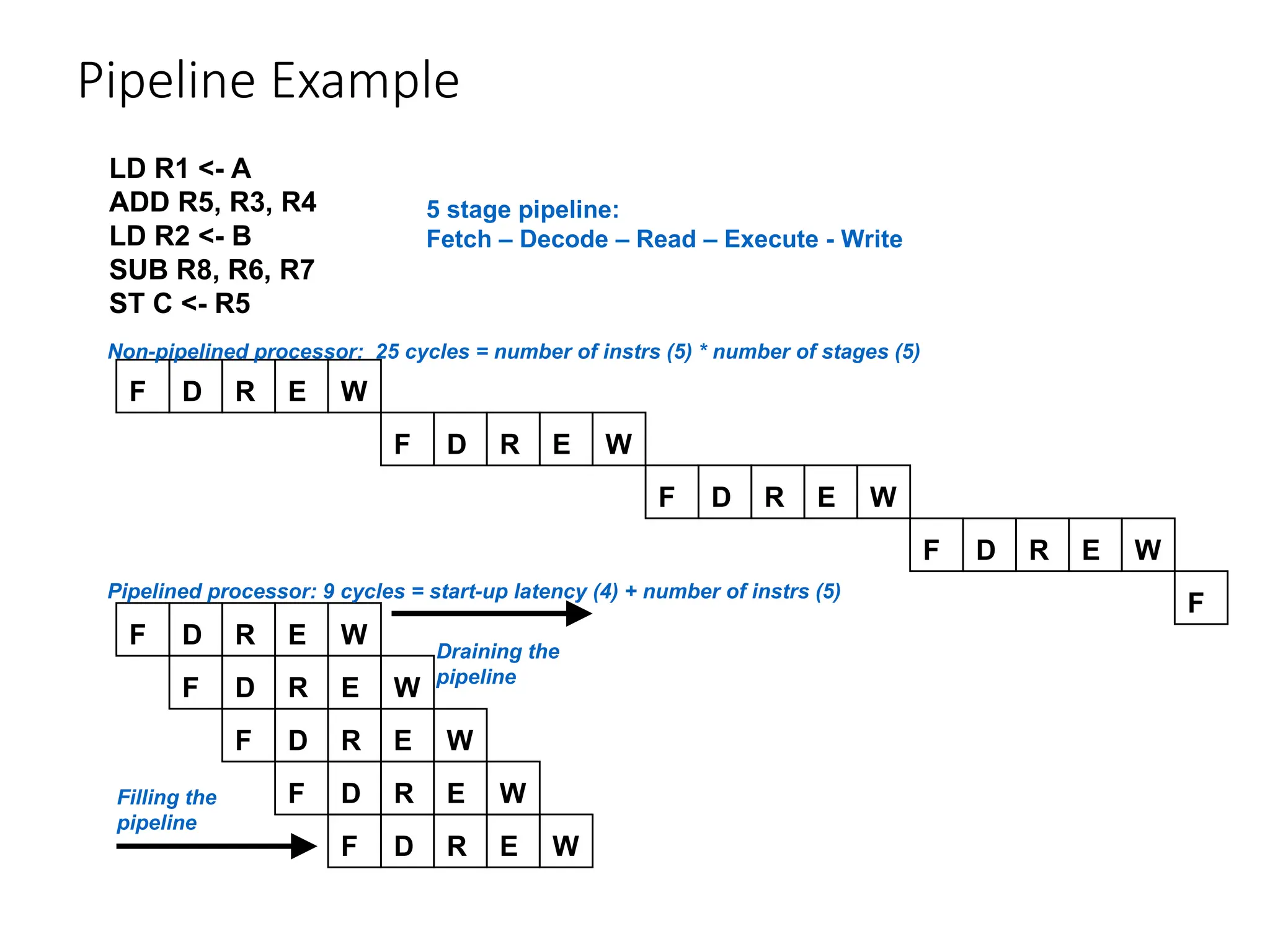
Pipeline Example
LD R1<- A
ADD R5, R3, R4
LD R2 <- B
SUB R8, R6, R7
ST C <- R5
F D R E W
F D R E W
F D R E W
F D R E W
F D R E W
F D R E W
F D R E W
F D R E W
F D R E W
F
Non-pipelined processor: 25 cycles = number of instrs (5) * number of stages (5)
Pipelined processor: 9 cycles = start-up latency (4) + number of instrs (5)
Filling the
pipeline
Draining the
pipeline
5 stage pipeline:
Fetch – Decode – Read – Execute - Write
50.
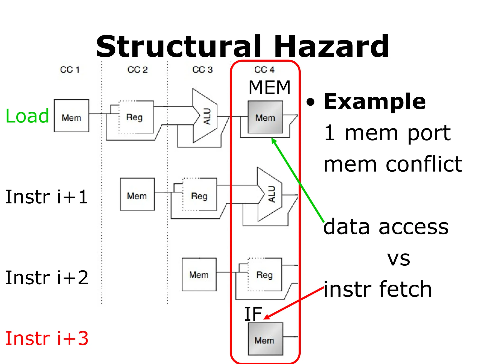
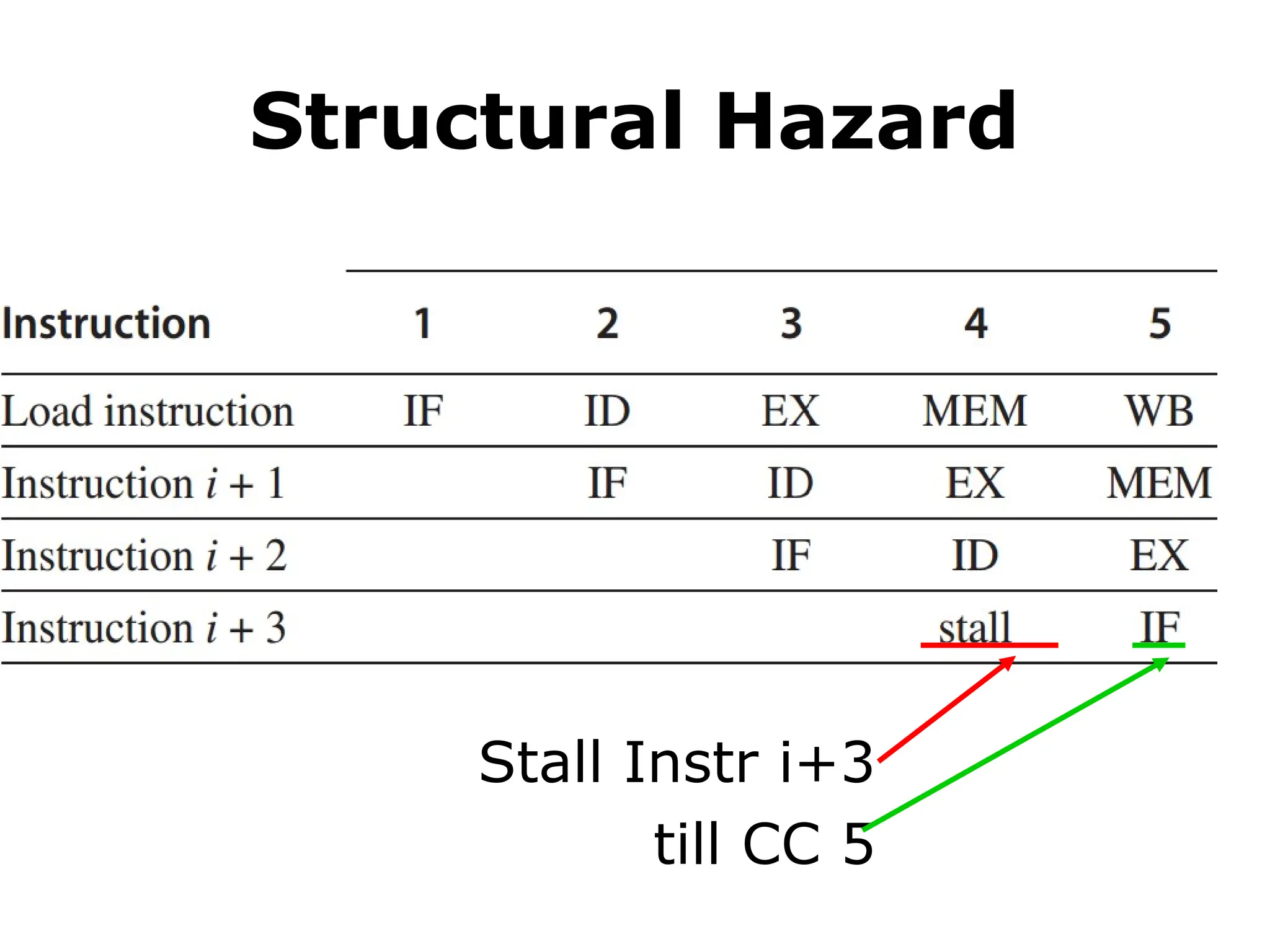
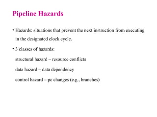
Pipeline Hazards
• Hazards:situations that prevent the next instruction from executing
in the designated clock cycle.
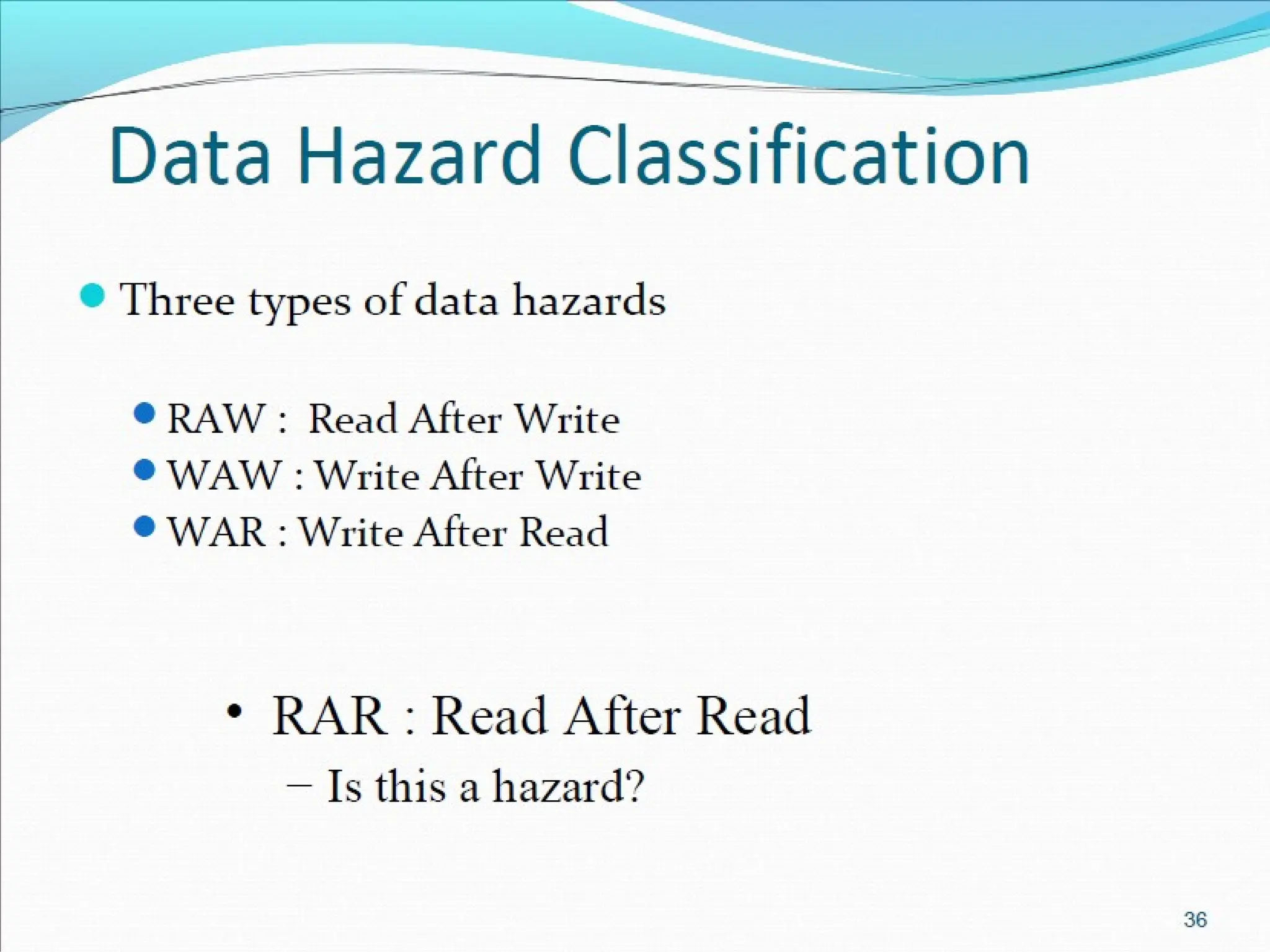
• 3 classes of hazards:
structural hazard – resource conflicts
data hazard – data dependency
control hazard – pc changes (e.g., branches)
51.
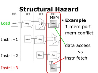
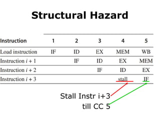
Structural Hazard
• Example
1mem port
mem conflict
data access
vs
instr fetch
Load
Instr i+3
Instr i+2
Instr i+1
MEM
IF
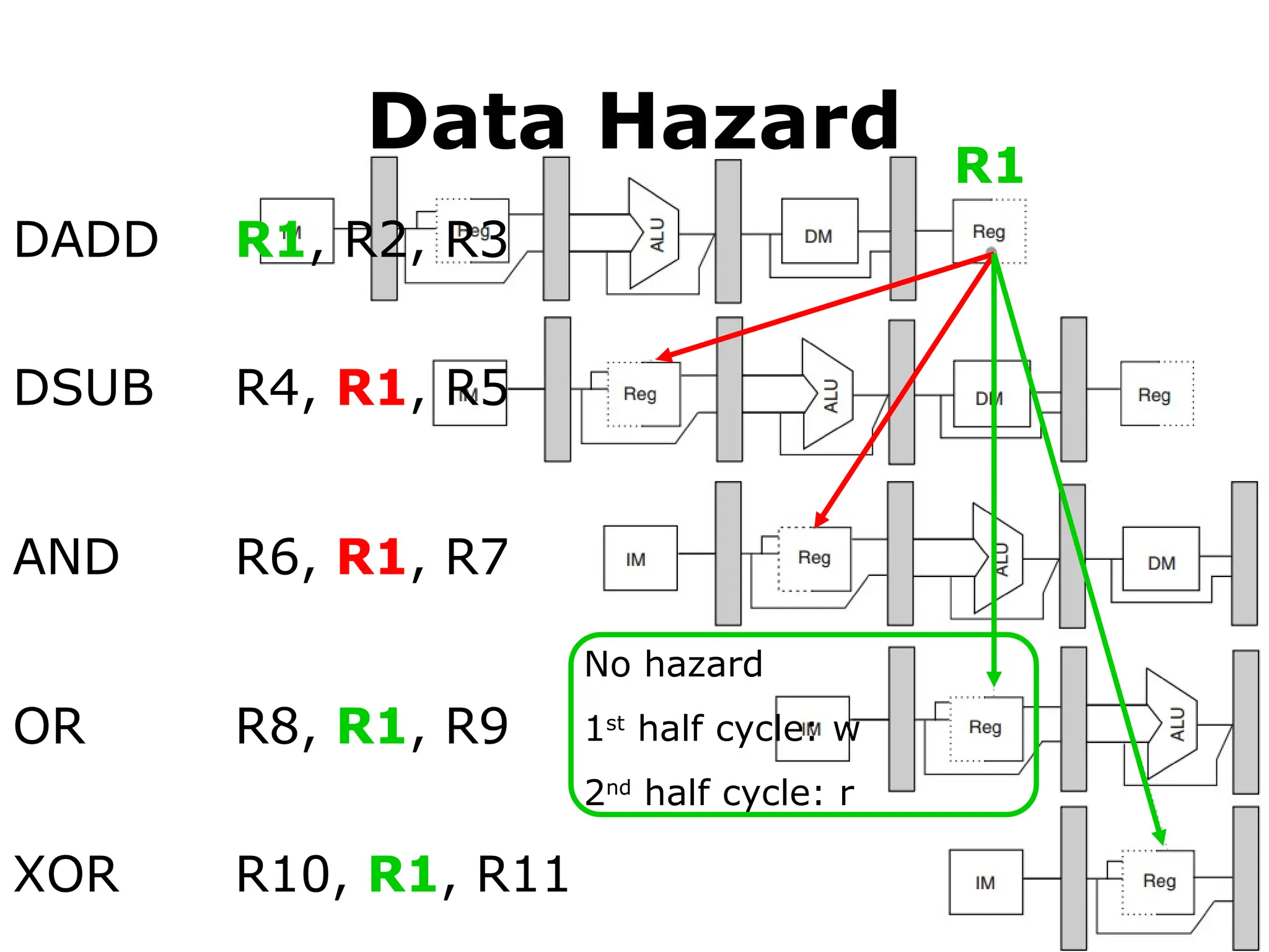
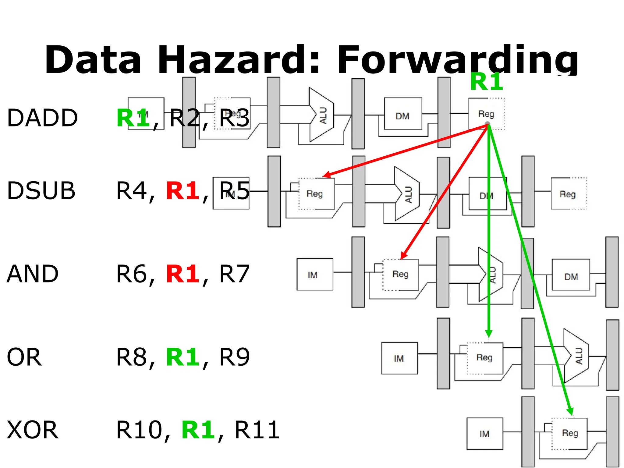
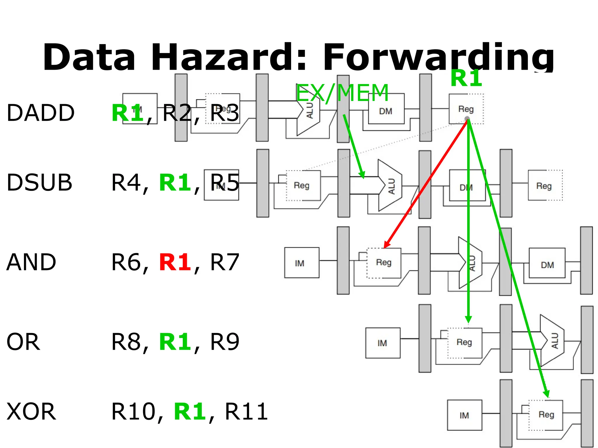
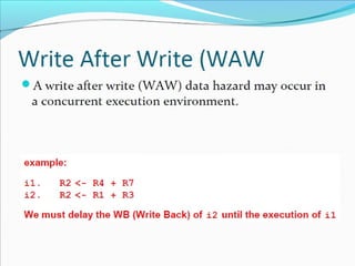
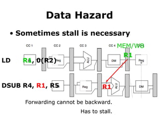
Data Hazard
• Sometimesstall is necessary
R1
R1
LD R1, 0(R2)
DSUB R4, R1, R5
MEM/WB
Forwarding cannot be backward.
Has to stall.
62.
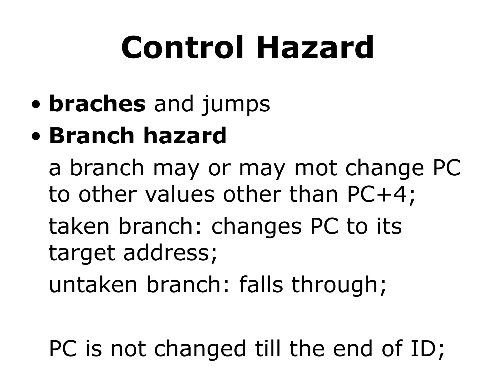
Control Hazard
• brachesand jumps
• Branch hazard
a branch may or may mot change PC
to other values other than PC+4;
taken branch: changes PC to its
target address;
untaken branch: falls through;
PC is not changed till the end of ID;
#51 Here’s an example of structural hazard due to memory conflict.
Assume the processor has only memory port.
A structural hazard will arise in clock cycle 4 when the load instruction reads data from memory and instruction i plus 3 fetches instruction from memory.
#52 The solution to this structural hazard is stall instruction i+3 for one clock cycle.
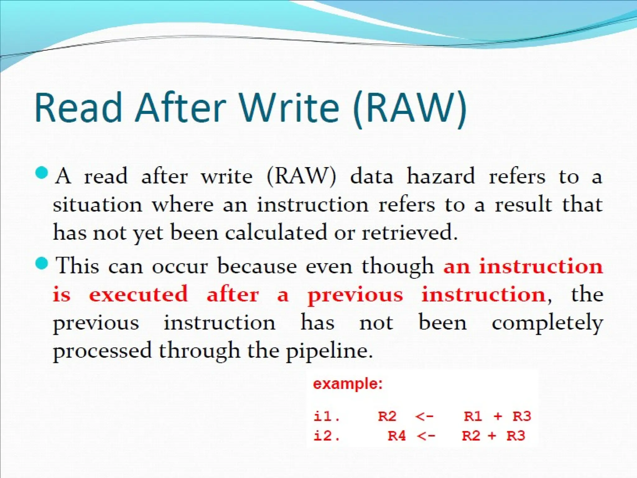
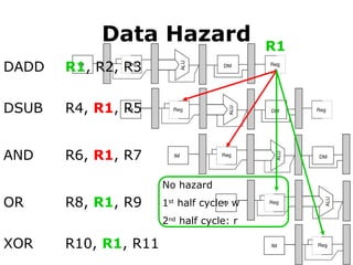
#57 In this example, the subtract and AND instructions need R1 before the add instruction prepares it. So R1 causes a data hazard that prevents normal pipelining of the subtract and AND instructions.
Note that the OR instruction has no hazard because the add instruction prepares R1 in the first half of the clock cycle while the OR instruction needs R1 till the second half.
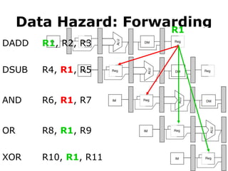
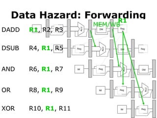
#59 The add instruction can directly provide the subtract instruction with R1 via its EX/MEM pipeline register.
#60 Similarly, the add instruction can provide the AND instruction with R1 via its MEM/WB pipeline register.
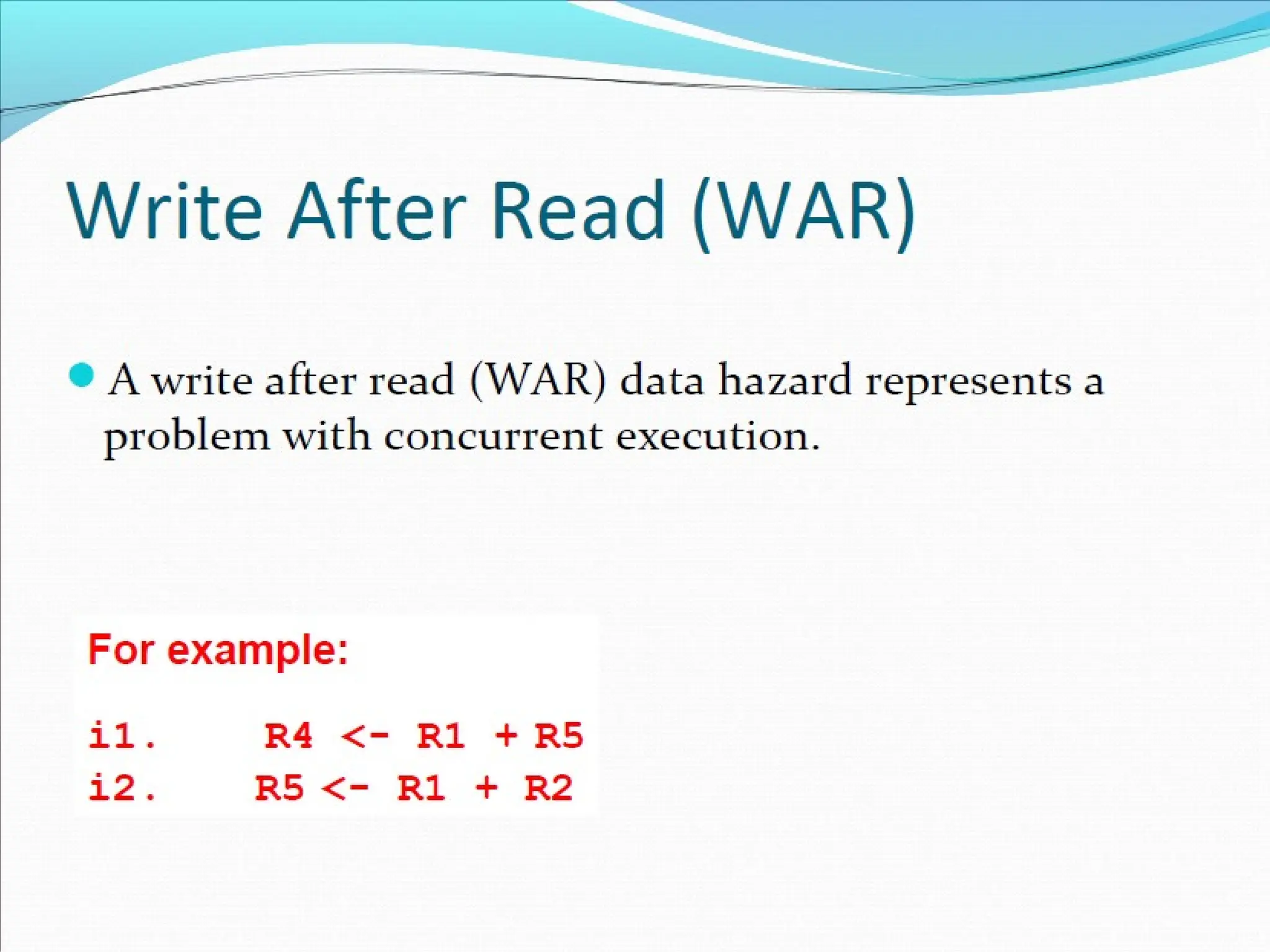
#61 But a stall is still necessary sometimes.
In this example, the load instruction prepares R1 till it reaches the MEM/WB pipeline register at the end of clock cycle 4.
The subtract instruction, however, requires R1 at the beginning of clock cycle 4. So in this case, no forwarding can be backward and thus the subtract instruction has to stall for one clock cycle.
#62 A control hazard happens to branches and jumps. In this lecture, we focus only on branches.
Its main reason is that a branch may or may not change program counter to other values other than PC+4 but the change is available till the end of ID clock cycle.
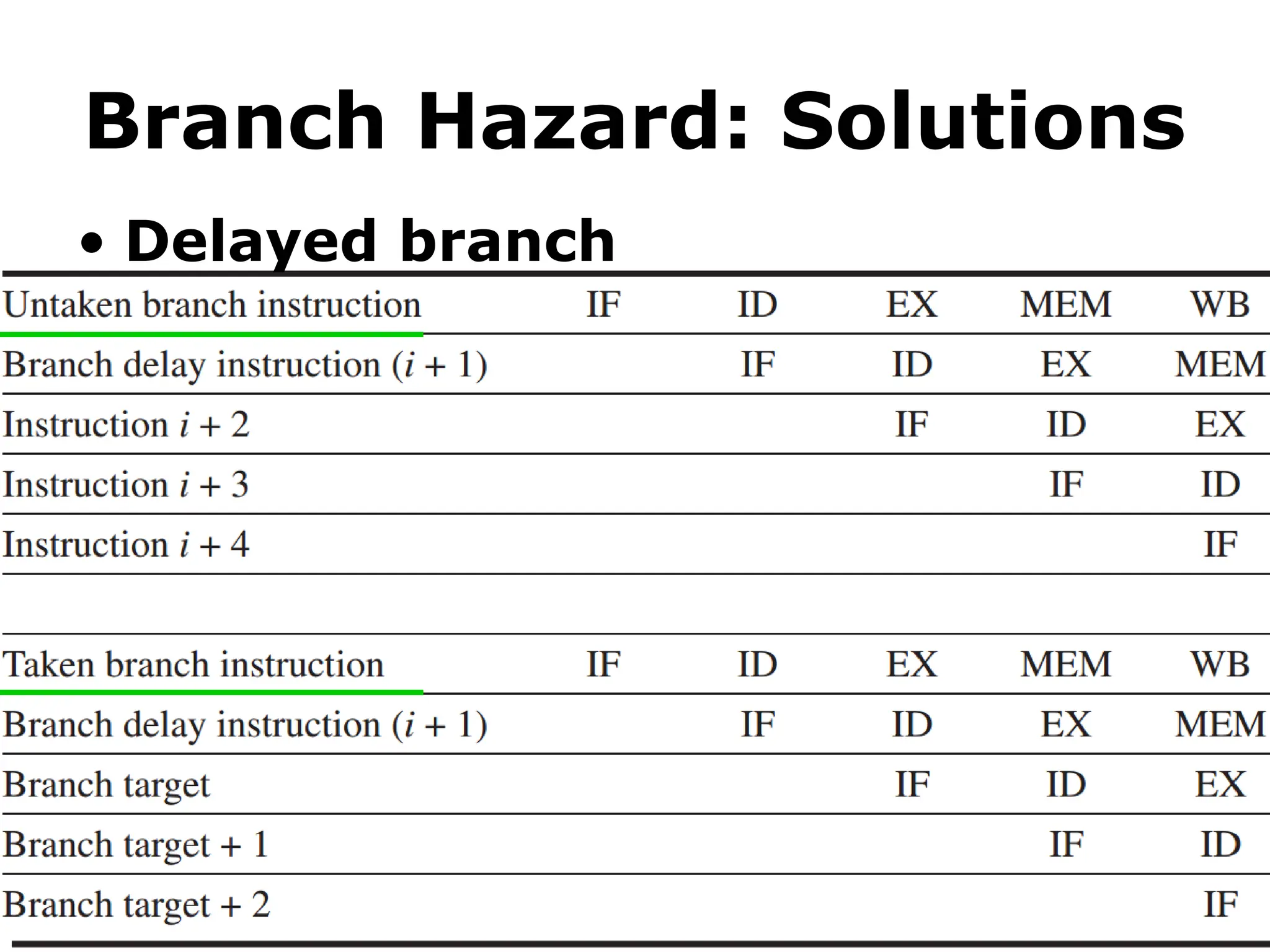
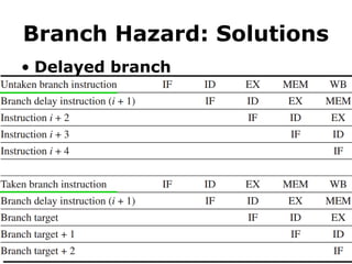
#63 Here are examples of delaying an untaken branch and a taken branch.
We can see that they have the same pipelining efficiency.


![Executing an Instruction
Fetch the contents of the memory location pointed to by
the PC. The contents of this location are loaded into the
IR (fetch phase).
IR ← [[PC]]
Assuming that the memory is byte addressable,
increment the contents of the PC by 4 (fetch phase).
PC ← [PC] + 4
Carry out the actions specified by the instruction in the
IR (execution phase).](https://image.slidesharecdn.com/unit4-250613110406-21835bfa/85/Computer-Organization-Unit-4-Processor-Control-Unit-4-320.jpg)
![3.Fetching a Word from Memory
The response time of each memory access varies (cache miss,
memory-mapped I/O,…).
To accommodate this, the processor waits until it receives an
indication that the requested operation has been completed
(Memory-Function-Completed, MFC).
Move (R1), R2
MAR ← [R1]
Start a Read operation on the memory bus
Wait for the MFC response from the memory
Load MDR from the memory bus
R2 ← [MDR]](https://image.slidesharecdn.com/unit4-250613110406-21835bfa/85/Computer-Organization-Unit-4-Processor-Control-Unit-17-320.jpg)


![Executing an Instruction
Fetch the contents of the memory location pointed to by
the PC. The contents of this location are loaded into the
IR (fetch phase).
IR ← [[PC]]
Assuming that the memory is byte addressable,
increment the contents of the PC by 4 (fetch phase).
PC ← [PC] + 4
Carry out the actions specified by the instruction in the
IR (execution phase).](https://image.slidesharecdn.com/unit4-250613110406-21835bfa/75/Computer-Organization-Unit-4-Processor-Control-Unit-4-2048.jpg)

![3.Fetching a Word from Memory
The response time of each memory access varies (cache miss,
memory-mapped I/O,…).
To accommodate this, the processor waits until it receives an
indication that the requested operation has been completed
(Memory-Function-Completed, MFC).
Move (R1), R2
MAR ← [R1]
Start a Read operation on the memory bus
Wait for the MFC response from the memory
Load MDR from the memory bus
R2 ← [MDR]](https://image.slidesharecdn.com/unit4-250613110406-21835bfa/75/Computer-Organization-Unit-4-Processor-Control-Unit-17-2048.jpg)