Download as PDF, PPTX


![8.References
[1] TJ Hammons, “Integrating renewable energy sources into Europeangrids,” International Journal of Electrical Power & Energy Systems,vol.
30,no. 8, pp. 462-475,2008.[2] Fen Lui and Yun Chen,“Design and control for three phase grid connected inverter with LCL filter,” Proceedings
of IEEE Circuits and Systems International conference,pp.1-4,2009.
[3] Mitra Mirhosseini, Josep Pou and Vassilios G. Agelidis,“Single- and Two-Stage Inverter Based Grid Connected Photovoltaic Power Plants
With Ride-Through Capability Under Grid Faults,” IEEE Transcations on Sustainable Energy, vol.6.,No.3.,July 2015.
[4] S.J.Huang and F.S.Pai,“Design and operation of grid connected phototvoltaicsystem with power factor control and active islanding
detection,” IEEE Proceedings on Generation, Transmission, Distribution,vol.48,No.2,2001.
[5] S.J.Huang and F.S.Pai,“Design and operation of grid connected phototvoltaic system with power factor control and active islanding
detection,” IEEE Proceedings on Generation, Transmission, Distribution, vol.48,No.2,2001.
[6] M. Castilla,J.Miret, A.Camacho, Jos´e Matas,De Vicuna and Luis Garc´ıa,“Reduction of current harmonic distortion in three-phase grid-
connected photovoltaic inverters via resonant current control,”IEEE Transactions on Industrial Electronics,VOL.60, No.4, pp.1464-1472,2013.
[7] T.Hornik and Qing-Chang Zhong ,“A Current-Control Strategy for Voltage-Source Inverters in Microgrids Based on and Repetitive
Control,”IEEE Transactions on Power Electronics,vol.26, No.3, pp.943-952,2011.
[8] T Q Zheng ,“Synchronous PI control for three-phase grid-connected photovoltaic inverter,” Proceedings of 2010 Chinese Control and
Decision Conference,2010.
[9] F. Ruza, A. Reyb, J.M. Torreloc, A. Nietob, F.J. Cnovasa,“Real time test benchmark design for photovoltaic grid-connected control systems,”
Electric Power Systems Research, Elseveir, vol.81,no, 4,pp. 907-914,2011.
[10] Mohammed A. Elgendy and Bashar Zahawi,“Assessment of the incremental conductance maximum power point tracking algorithm,” IEEE
Transactions on Sustainable Energy, vol. 4,no. 1, pp. 108-117,2013.
[11] Kaura and V. Blasko,“Operation of a Phase Locked Loop System Under Distorted Utility Conditions,” Eleventh Annual Proceedings of
Applied Power Electronics Conference and Exposition,vol.2,pp.703-708,1996.
[12] L. Hadjidemetriou, E. Kyriakides, and F. Blaabjerg,“A new hybrid PLL for interconnecting Renewable Energy Systems to the grid,” IEEE
Energy Conversion Congress and Exposition,pp.20752082,2012.
[13] Dean Banerjee,“PLL Performance, Simulation and Design,” 4th Edition,Dog Ear Publishing
[14] “System Generator User Guide,”Documentation, XILINX
3/5/2016 24](https://image.slidesharecdn.com/paperid168-161119022655/85/Multi-string-PV-array-24-320.jpg)


![8.References
[1] TJ Hammons, “Integrating renewable energy sources into Europeangrids,” International Journal of Electrical Power & Energy Systems,vol.
30,no. 8, pp. 462-475,2008.[2] Fen Lui and Yun Chen,“Design and control for three phase grid connected inverter with LCL filter,” Proceedings
of IEEE Circuits and Systems International conference,pp.1-4,2009.
[3] Mitra Mirhosseini, Josep Pou and Vassilios G. Agelidis,“Single- and Two-Stage Inverter Based Grid Connected Photovoltaic Power Plants
With Ride-Through Capability Under Grid Faults,” IEEE Transcations on Sustainable Energy, vol.6.,No.3.,July 2015.
[4] S.J.Huang and F.S.Pai,“Design and operation of grid connected phototvoltaicsystem with power factor control and active islanding
detection,” IEEE Proceedings on Generation, Transmission, Distribution,vol.48,No.2,2001.
[5] S.J.Huang and F.S.Pai,“Design and operation of grid connected phototvoltaic system with power factor control and active islanding
detection,” IEEE Proceedings on Generation, Transmission, Distribution, vol.48,No.2,2001.
[6] M. Castilla,J.Miret, A.Camacho, Jos´e Matas,De Vicuna and Luis Garc´ıa,“Reduction of current harmonic distortion in three-phase grid-
connected photovoltaic inverters via resonant current control,”IEEE Transactions on Industrial Electronics,VOL.60, No.4, pp.1464-1472,2013.
[7] T.Hornik and Qing-Chang Zhong ,“A Current-Control Strategy for Voltage-Source Inverters in Microgrids Based on and Repetitive
Control,”IEEE Transactions on Power Electronics,vol.26, No.3, pp.943-952,2011.
[8] T Q Zheng ,“Synchronous PI control for three-phase grid-connected photovoltaic inverter,” Proceedings of 2010 Chinese Control and
Decision Conference,2010.
[9] F. Ruza, A. Reyb, J.M. Torreloc, A. Nietob, F.J. Cnovasa,“Real time test benchmark design for photovoltaic grid-connected control systems,”
Electric Power Systems Research, Elseveir, vol.81,no, 4,pp. 907-914,2011.
[10] Mohammed A. Elgendy and Bashar Zahawi,“Assessment of the incremental conductance maximum power point tracking algorithm,” IEEE
Transactions on Sustainable Energy, vol. 4,no. 1, pp. 108-117,2013.
[11] Kaura and V. Blasko,“Operation of a Phase Locked Loop System Under Distorted Utility Conditions,” Eleventh Annual Proceedings of
Applied Power Electronics Conference and Exposition,vol.2,pp.703-708,1996.
[12] L. Hadjidemetriou, E. Kyriakides, and F. Blaabjerg,“A new hybrid PLL for interconnecting Renewable Energy Systems to the grid,” IEEE
Energy Conversion Congress and Exposition,pp.20752082,2012.
[13] Dean Banerjee,“PLL Performance, Simulation and Design,” 4th Edition,Dog Ear Publishing
[14] “System Generator User Guide,”Documentation, XILINX
3/5/2016 24](https://image.slidesharecdn.com/paperid168-161119022655/75/Multi-string-PV-array-24-2048.jpg)


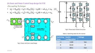
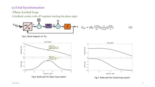
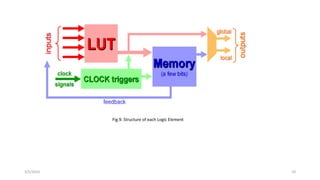
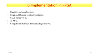
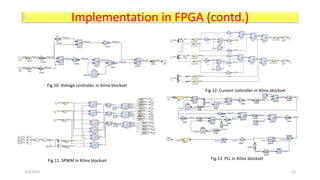
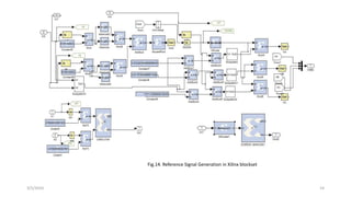
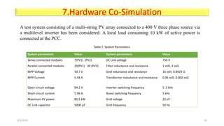
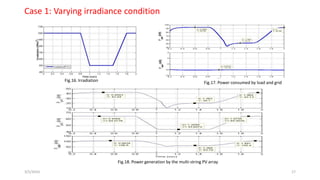
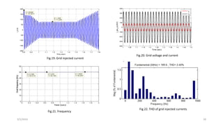
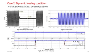
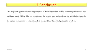
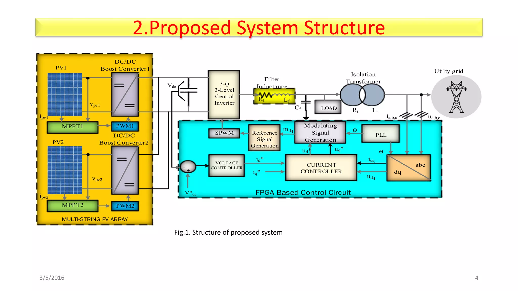
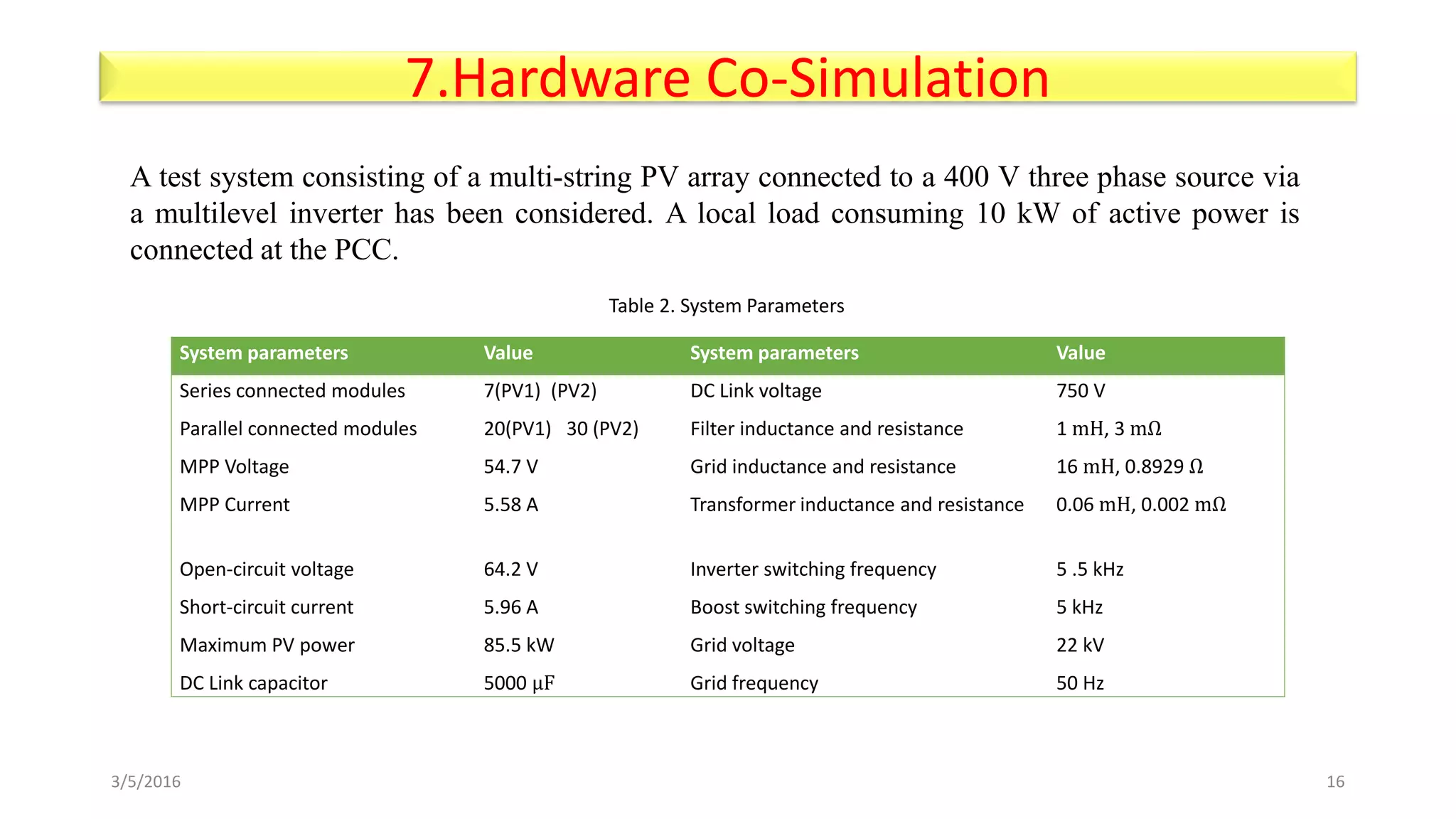
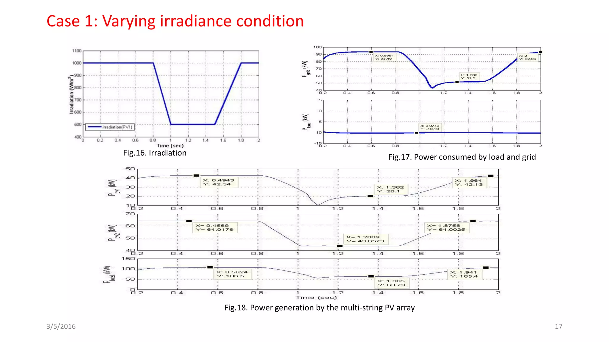
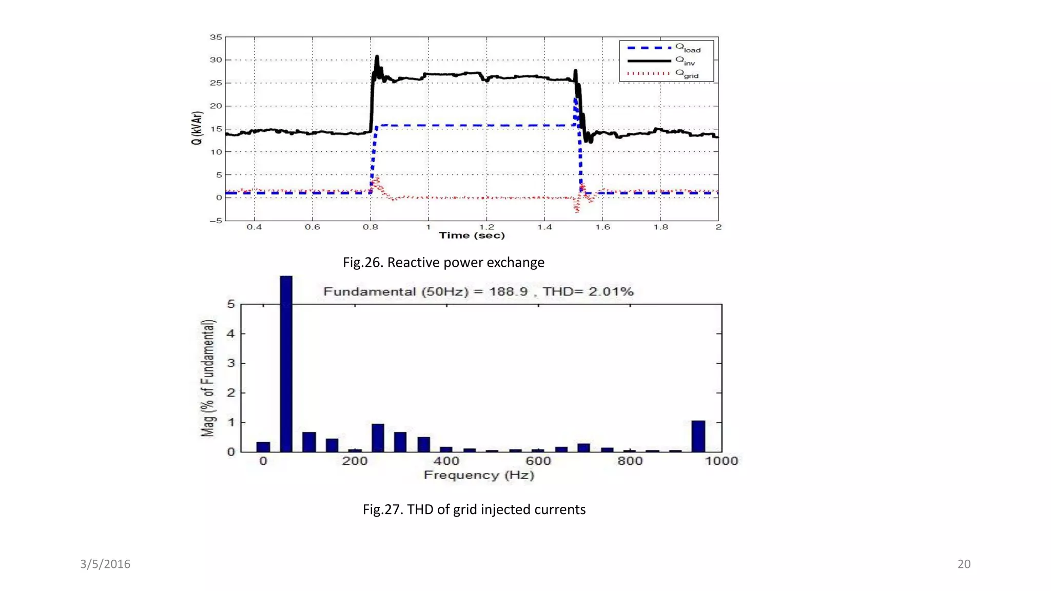
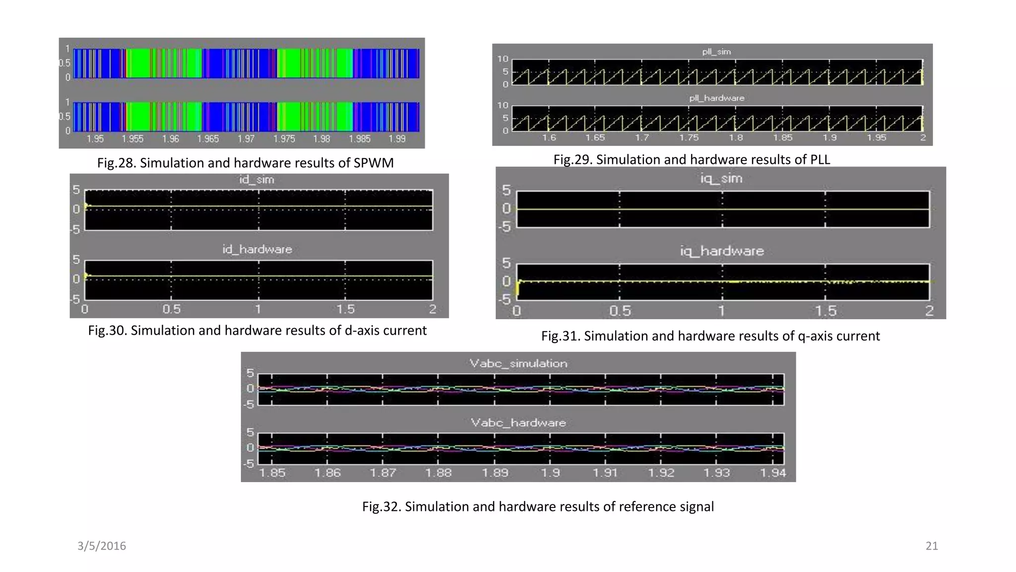
The document describes a real-time analysis and simulation of a multi-string grid-connected photovoltaic inverter using an FPGA. It proposes a system structure with multiple PV arrays connected to a 3-level central inverter. It discusses control algorithms including maximum power point tracking and voltage/current control loops. The system is implemented on an FPGA using Xilinx System Generator. Hardware co-simulation results validate the real-time performance of the proposed system.


