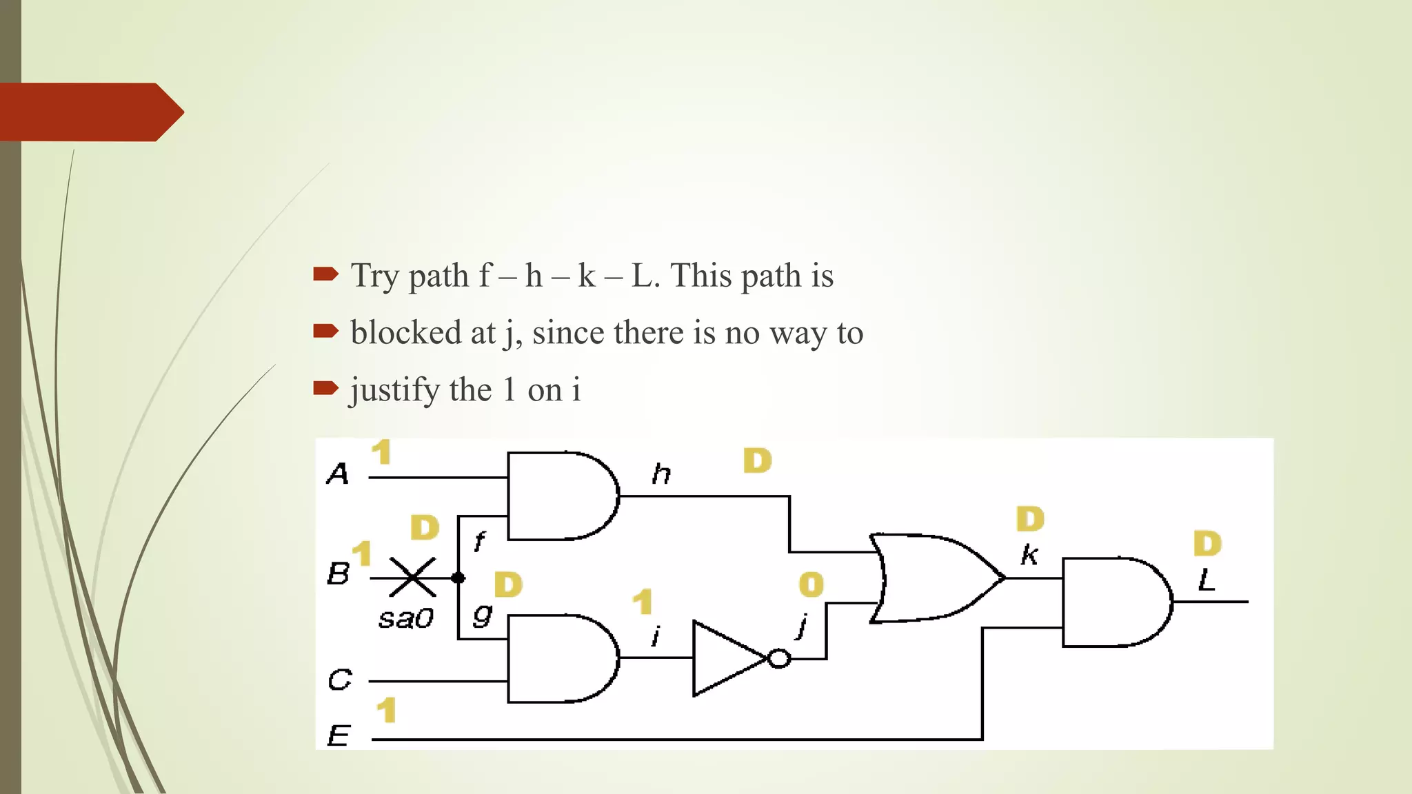
Download as PDF, PPTX
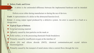


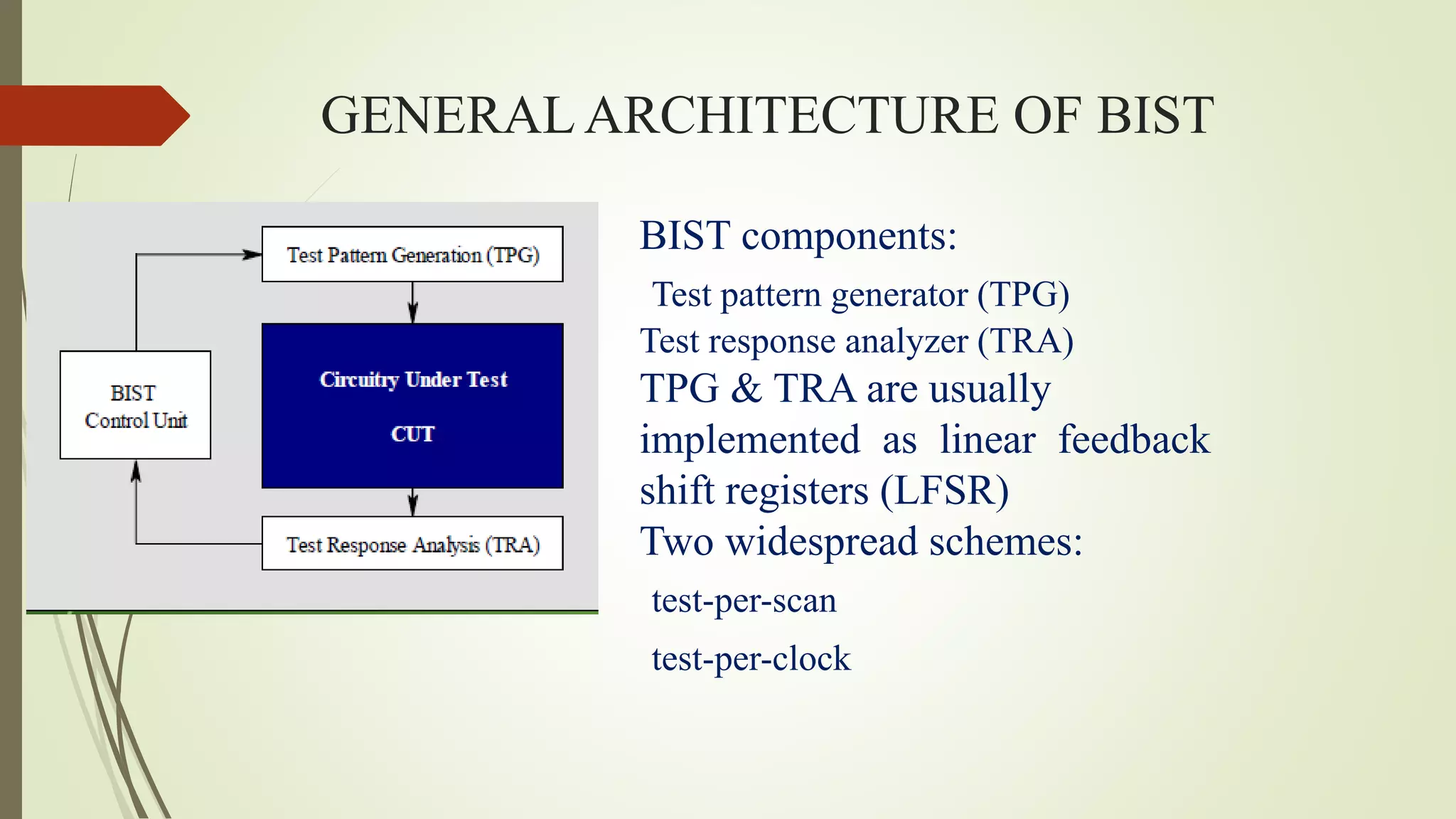


This document discusses VLSI testing and analysis. It defines key terms like defect, fault, and error and describes typical types of defects. It also discusses logical fault models and the role of testing in quality control. Different types of tests like production testing and burn-in testing are described. The testing process, fault simulation, design for testability techniques, and built-in self-test are summarized.


![Design for Test [DFT]-1 (1).pdf DESIGN DFT](https://cdn.slidesharecdn.com/ss_thumbnails/designfortestdft-11-231227151941-28a508a3-thumbnail.jpg?width=600ounds&width=560&fit=bounds)


