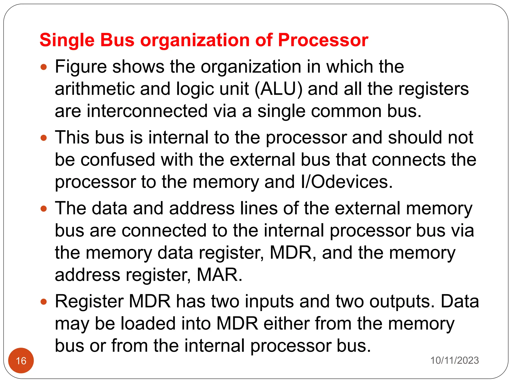
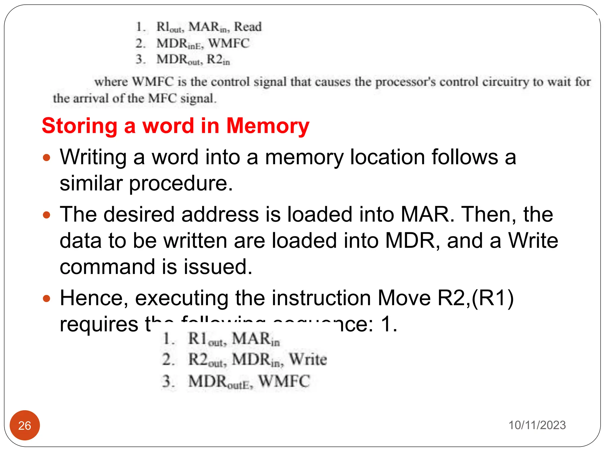
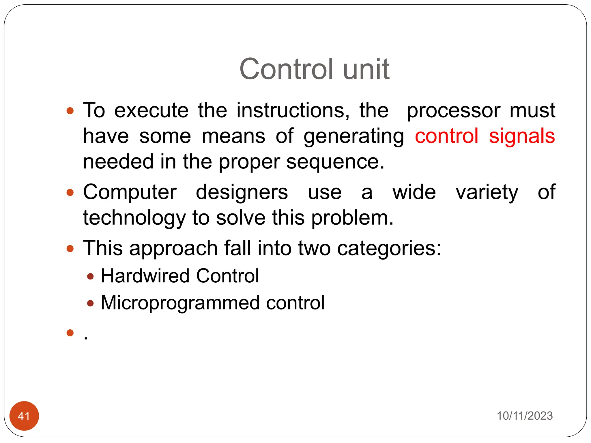
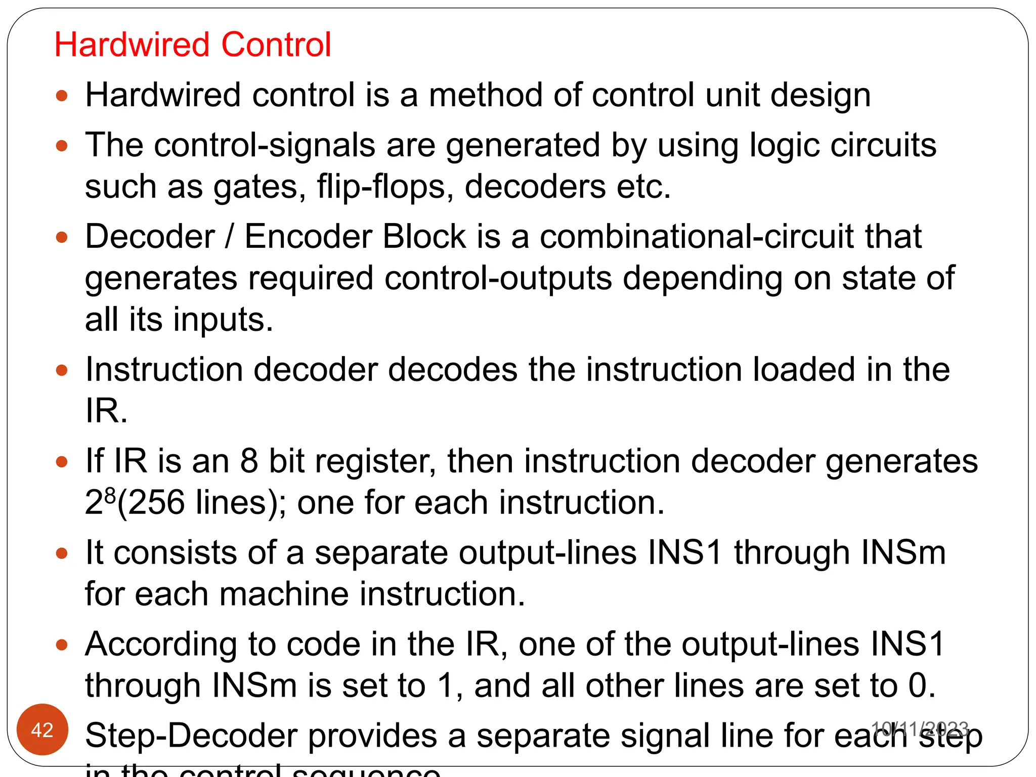
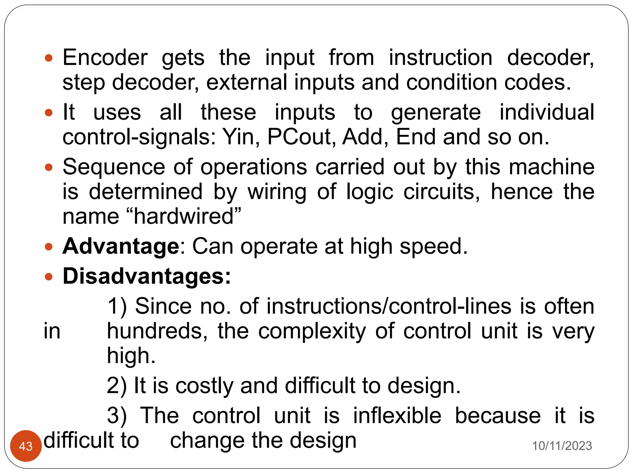
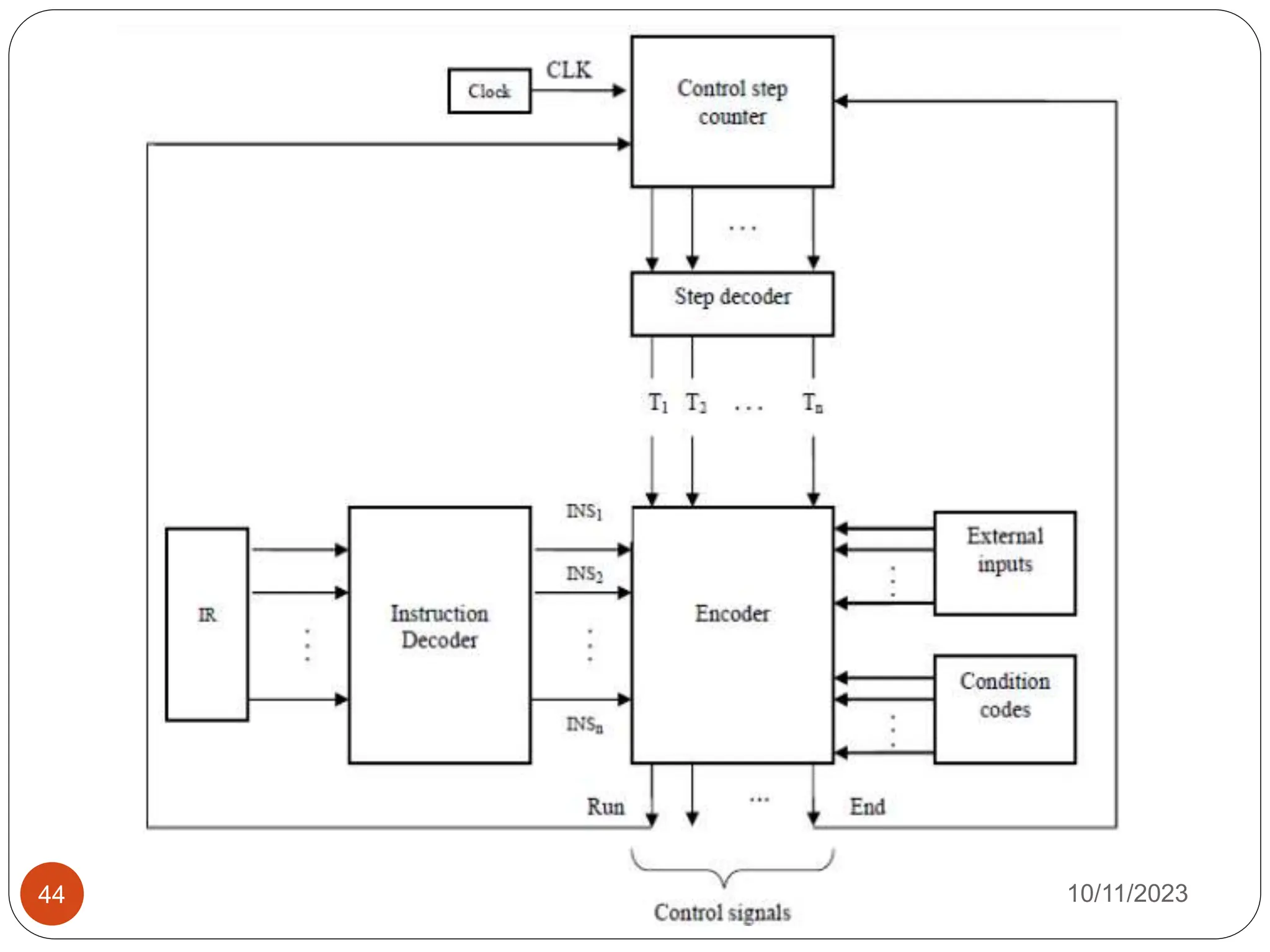
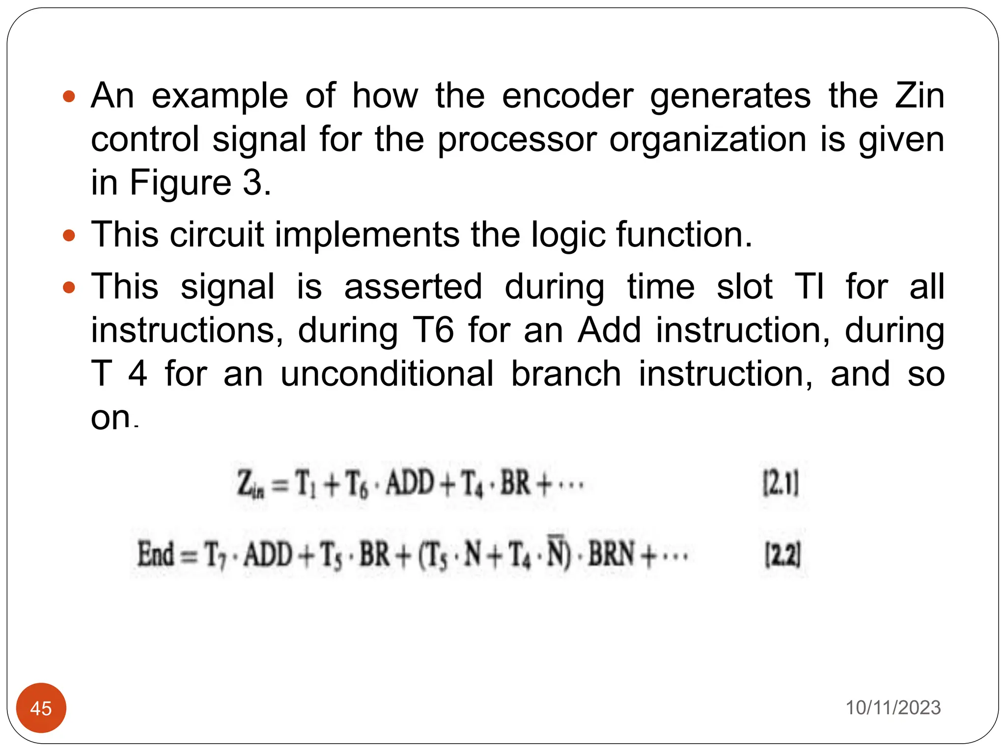
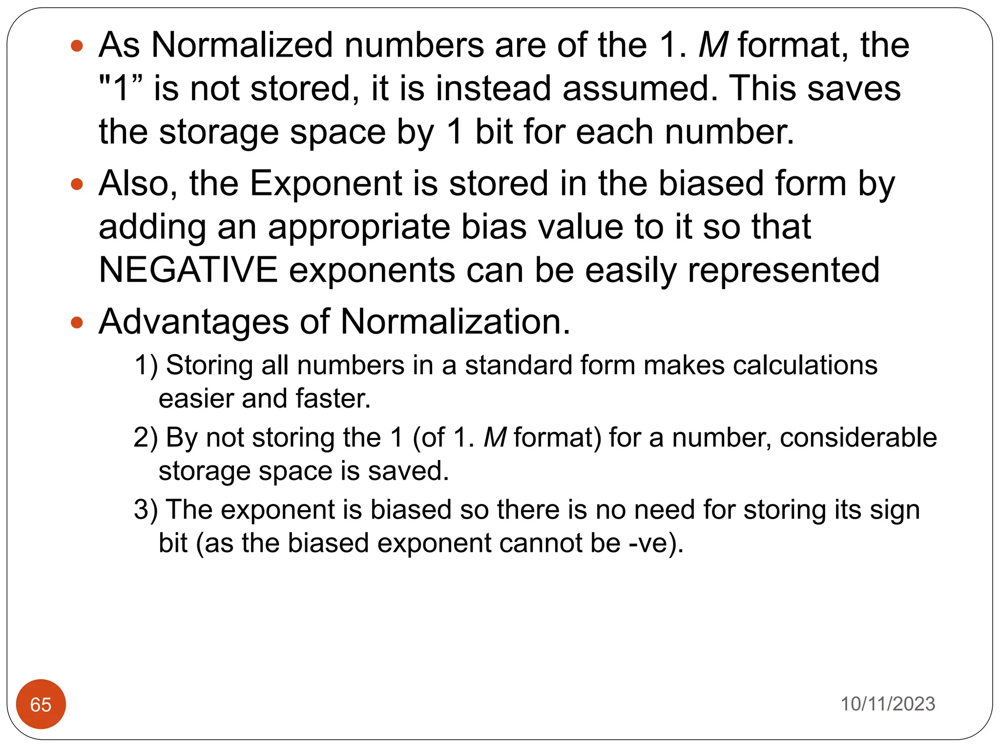
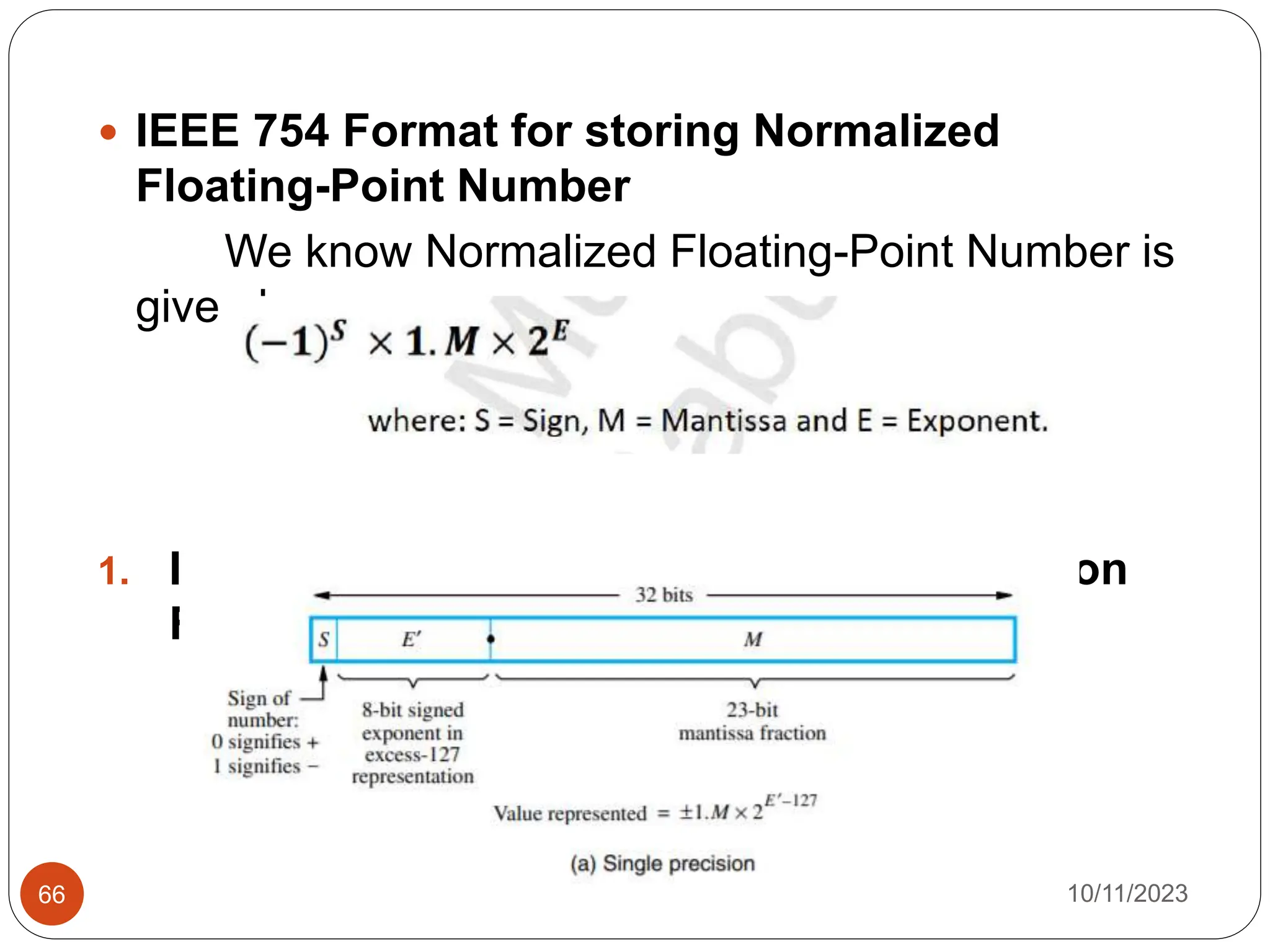
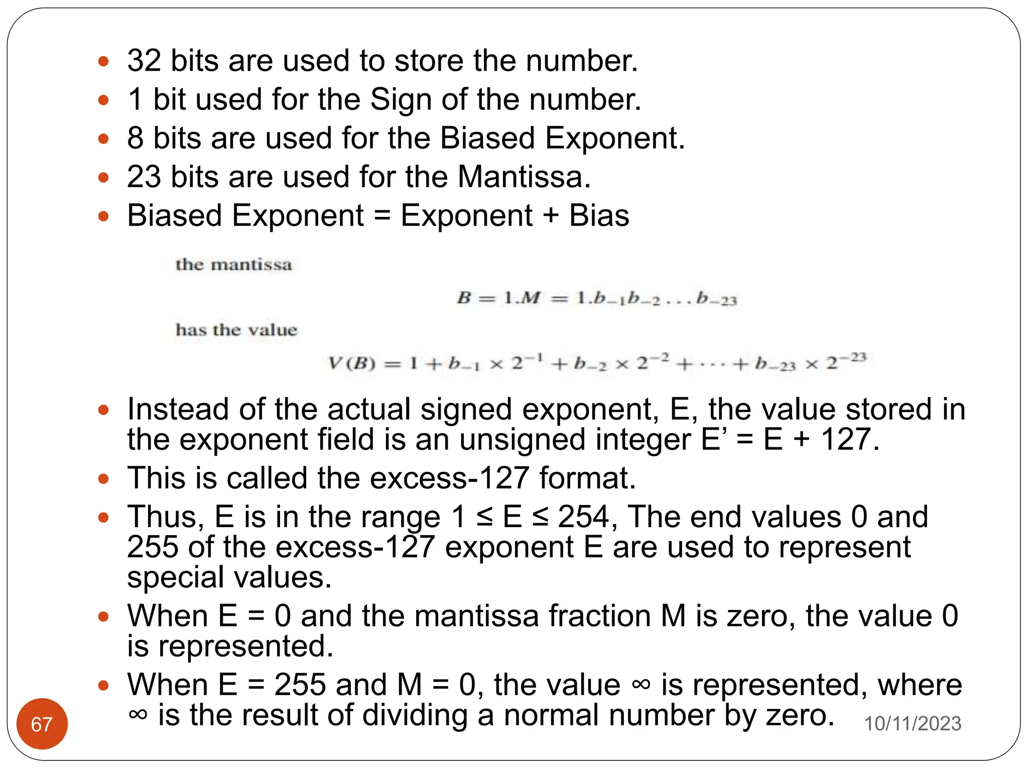
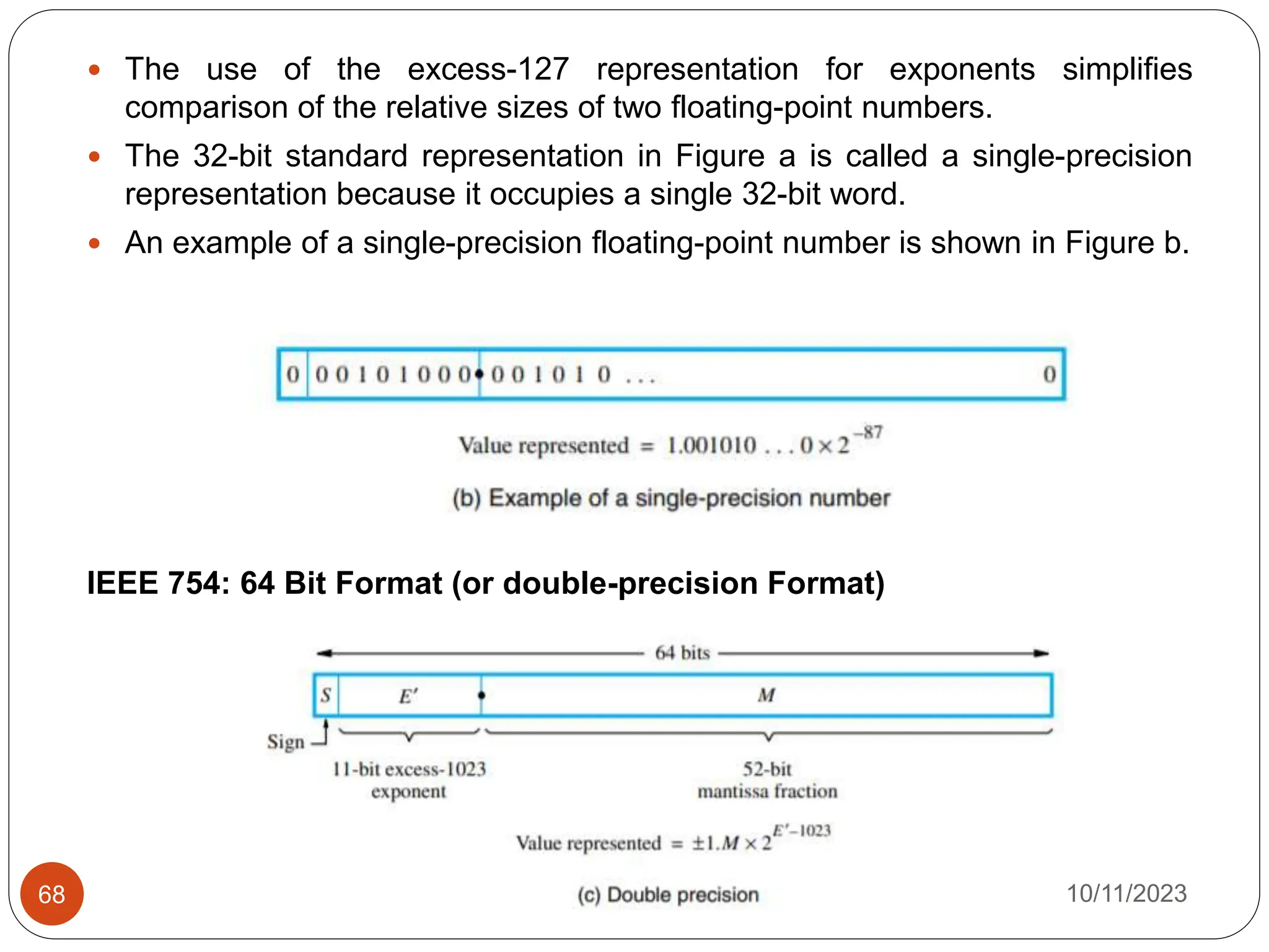
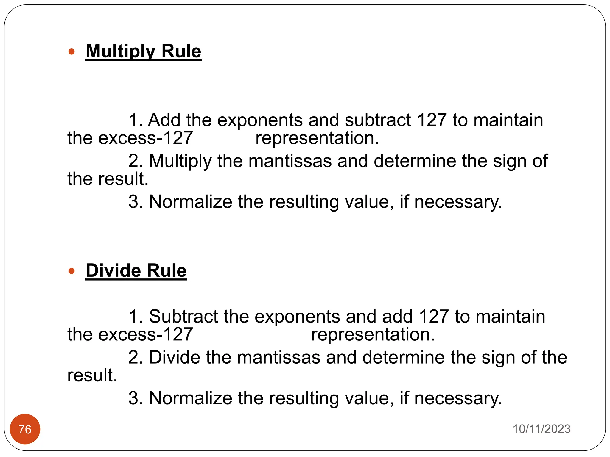
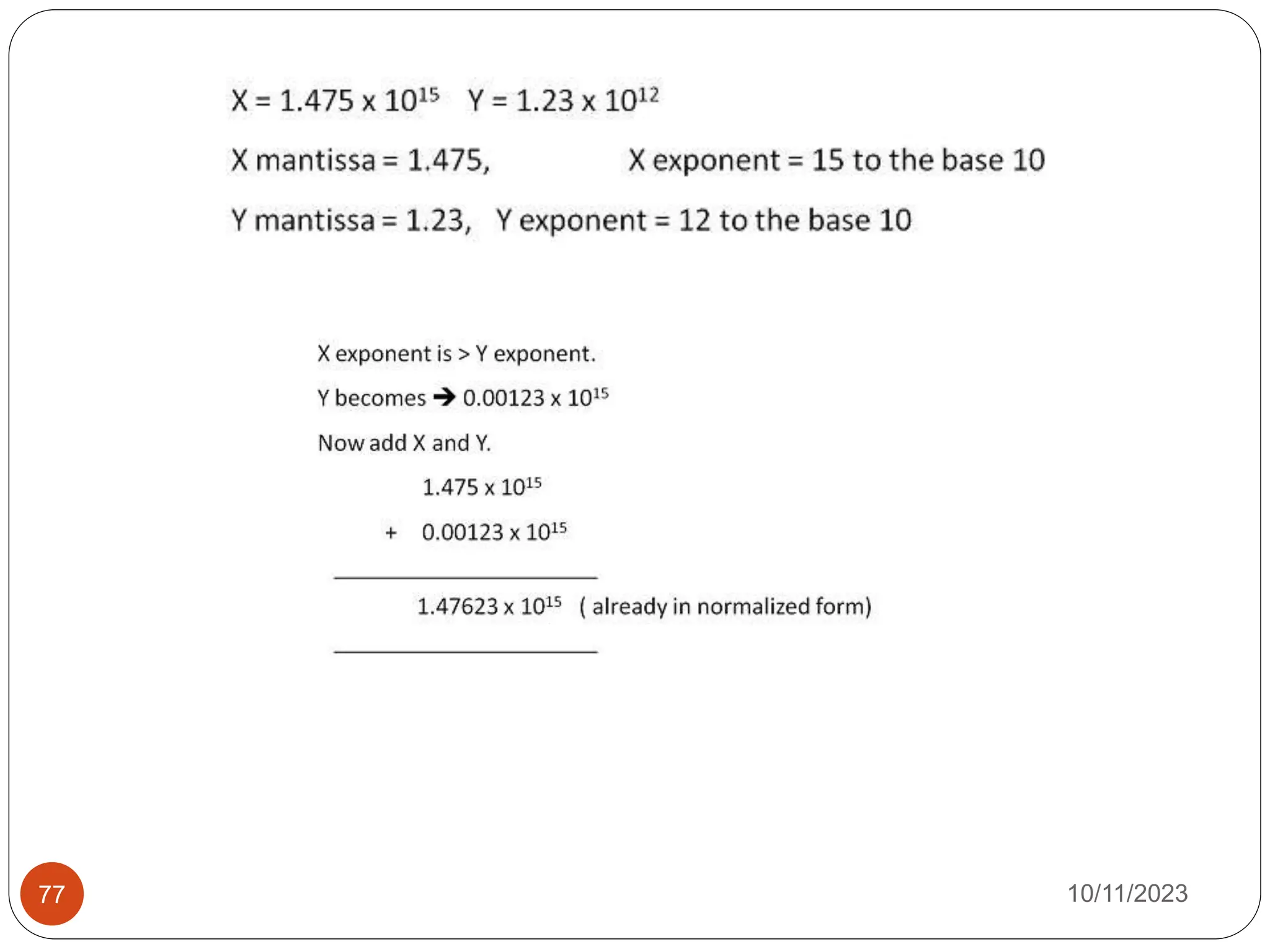
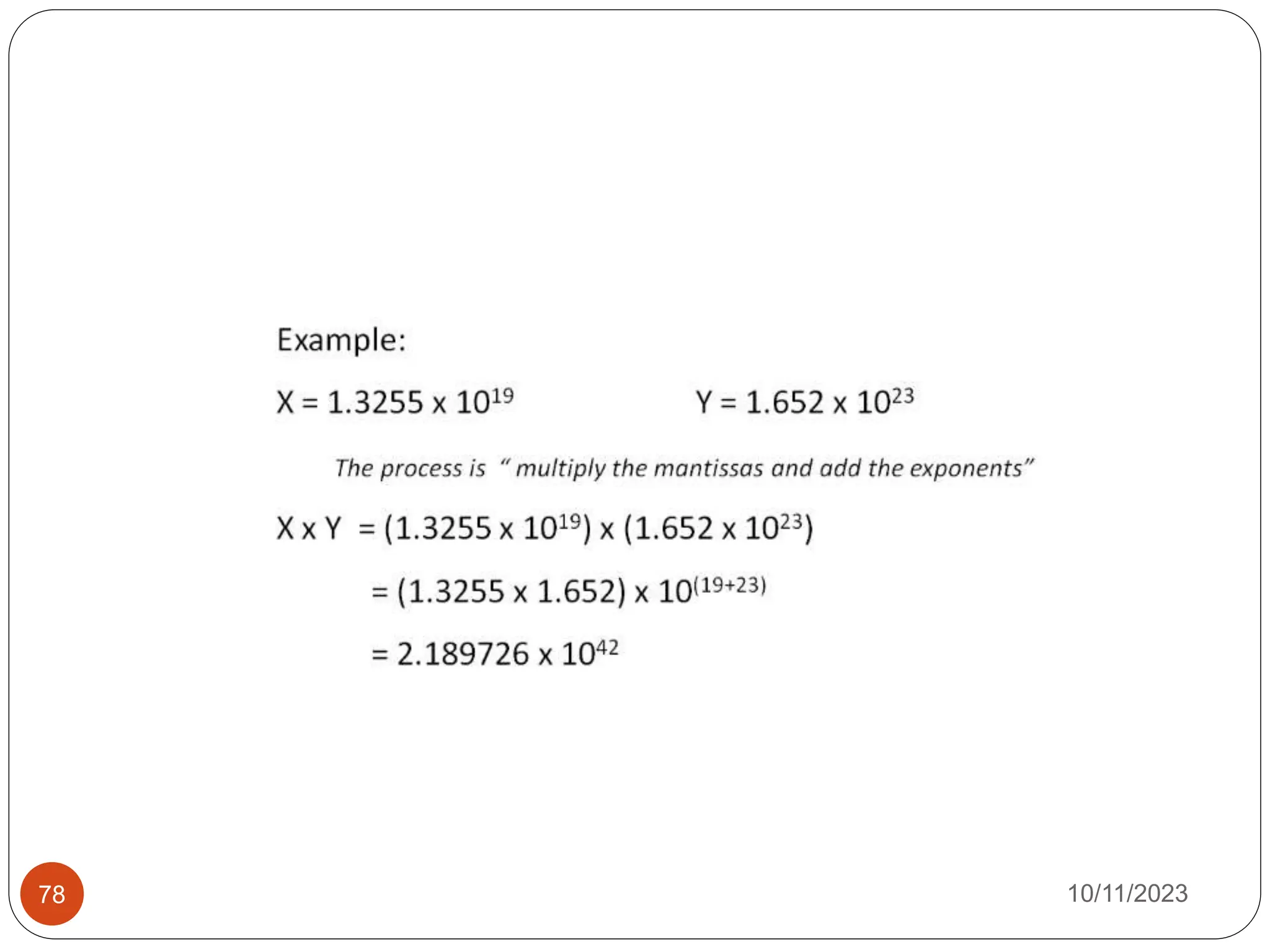
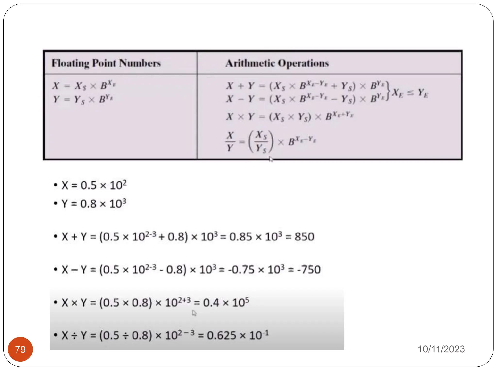
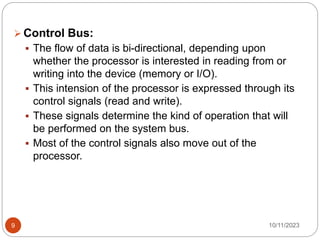
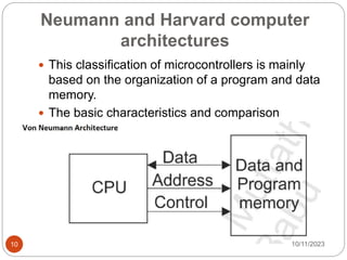
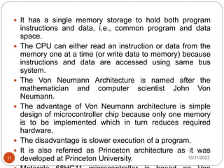
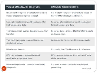
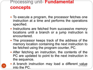
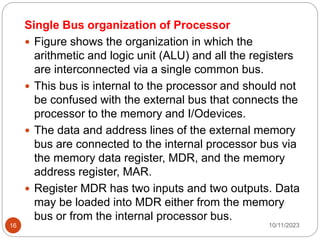
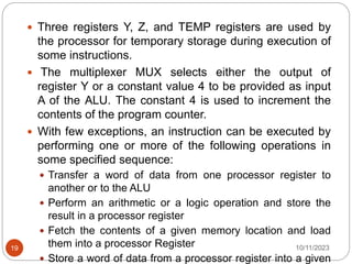
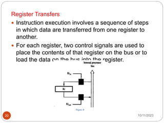
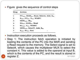
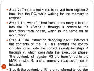
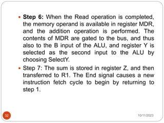
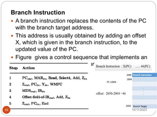
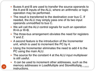
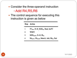
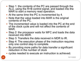
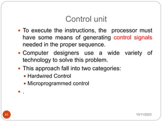
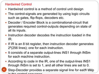
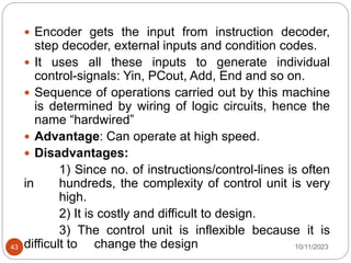
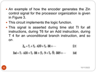
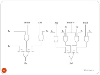
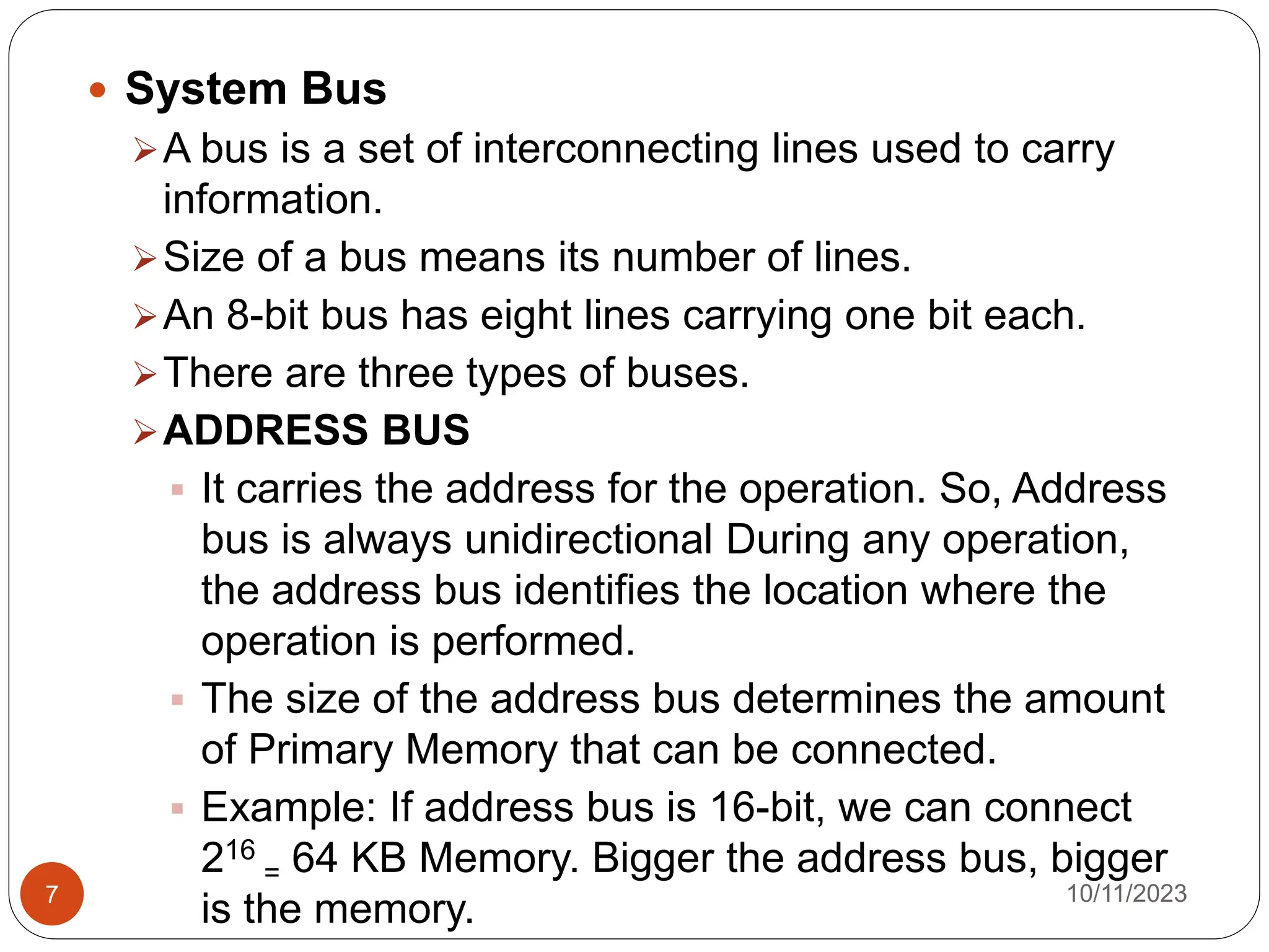
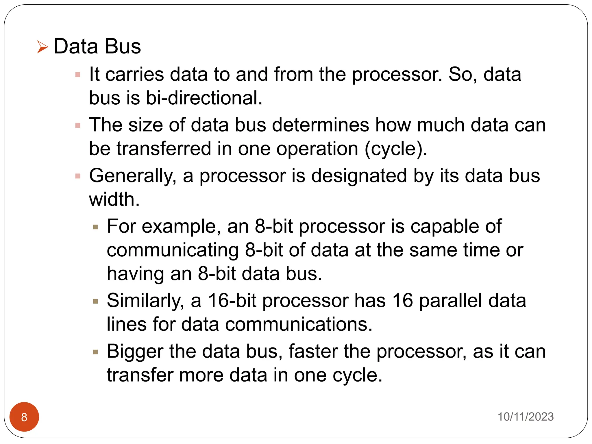
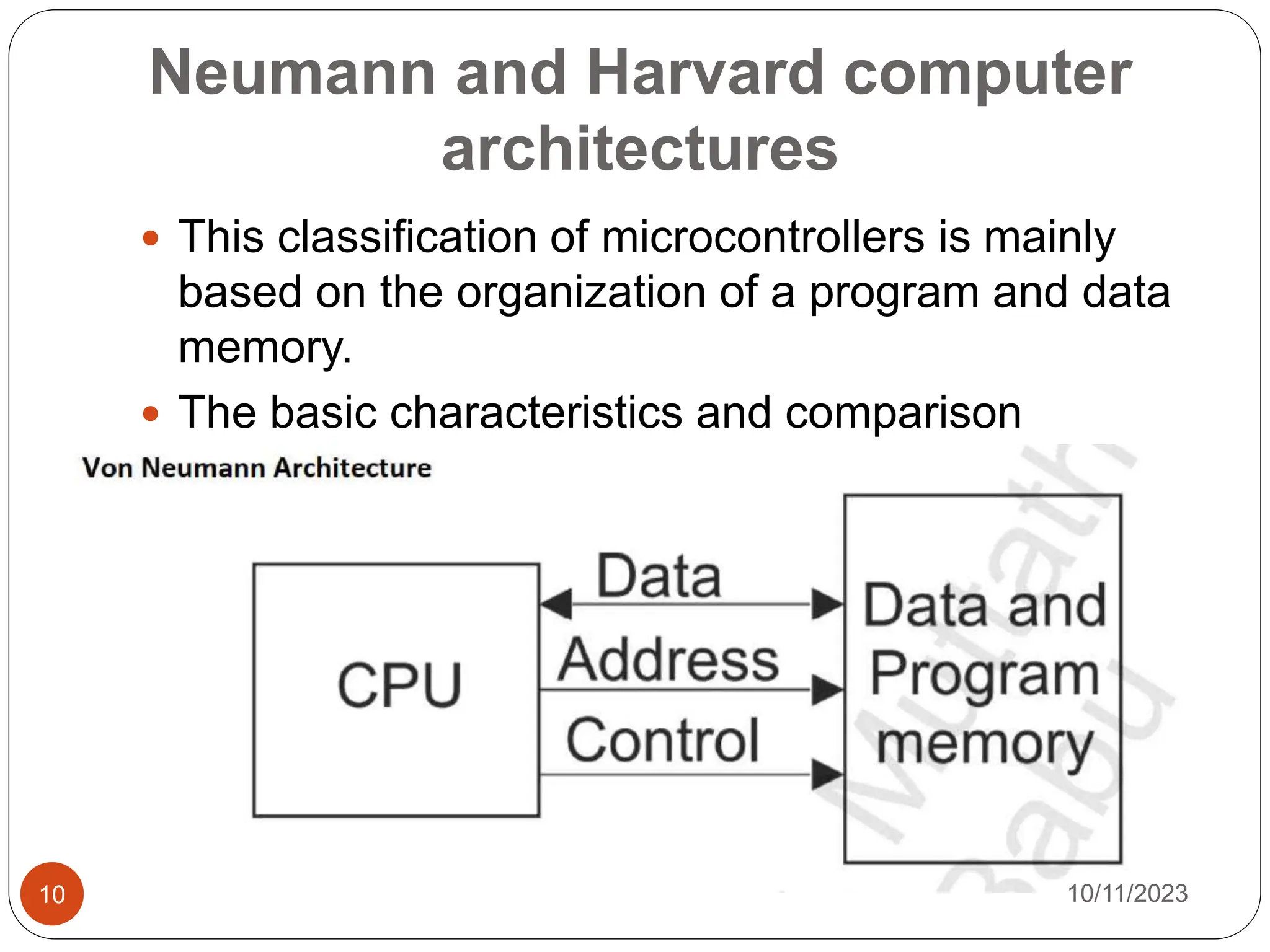
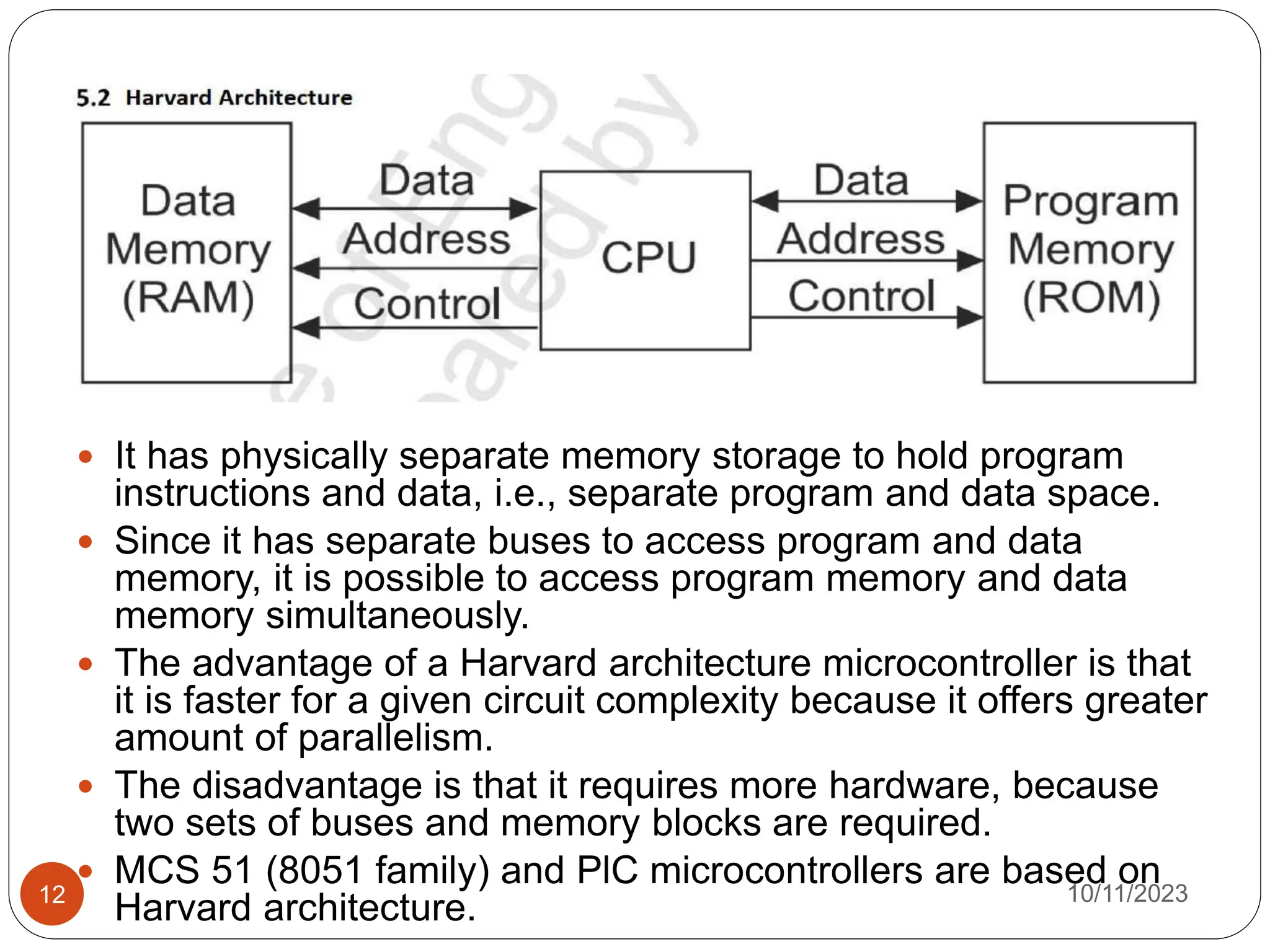
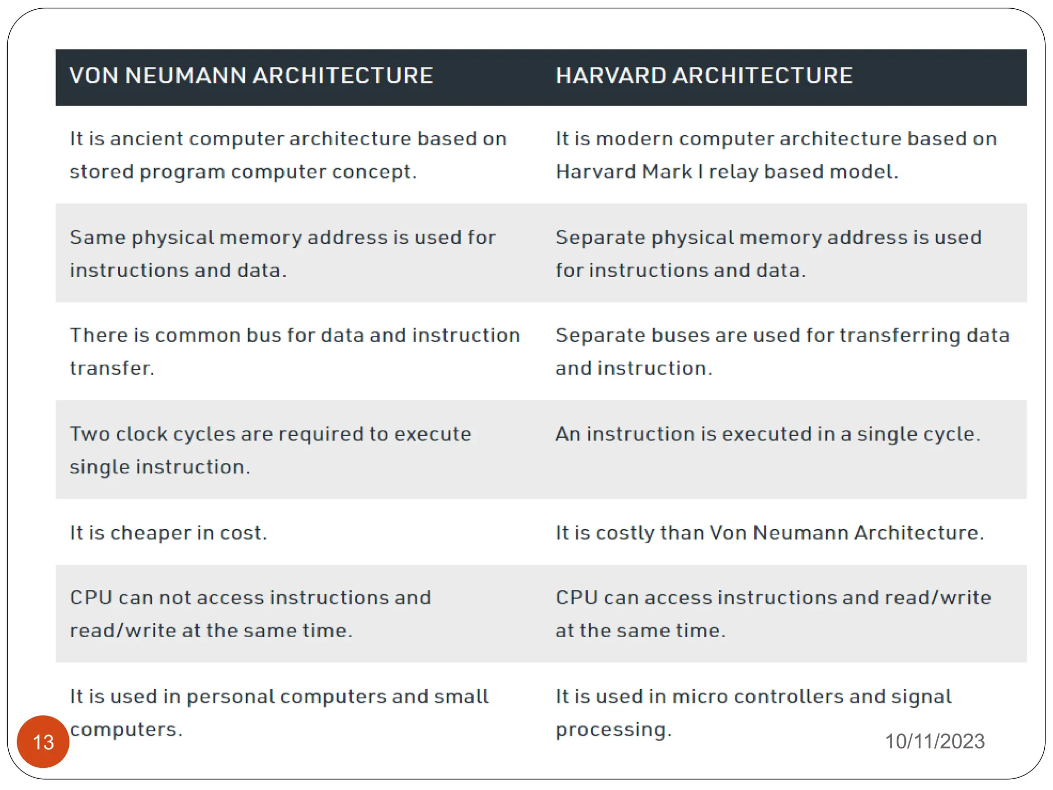
KEMBAR78
Computer Arithmetic and Processor Basics | PPTX
Module 1: Computer Arithmetic and Processor Basics
Functional architectures,. Hardwired
Control, Multiple Bus organization, other enhancements Microprogrammed
control. Number
representations - Fixed and floating point-number representation, Arithmetic
operations on
floating
point numbers
MODULE 1
10/11/2023
1
Functional units of a computer
10/11/2023
2
 A computer system mainly consists of the CPU, Memory,
I/O devices and the System bus used for Interconnections.
 CPU
 The Central Processing Unit is the brain of a computer
 It is also called the microprocessor or simply the processor.
 It consists of the ALU, Registers, Control Unit etc.
 All programs are executed in the CPU.
 A program is a set of instructions stored in the memory.
 The main function of the CPU is to fetch, decode and execute
these instructions.
 Instructions are fetched from the memory using the various
buses.
 Thereafter they are decoded by the Control Unit to analyze
the Opcode.
 Finally, the instruction is executed to perform the desired
operation.
 This execution mainly involves the ALU and the internal
registers of the processor 10/11/2023
3
 MEMORY
 The memory is used to store information.
 It mainly stores programs and data.
 Memory has various locations.
 Each location is identified by its own unique address and
contains some data.
 The most basic form of memory is called Primary Memory,
which consists of RAM and ROM.
 Primary (or main) Memory stores programs along with data,
which are to be executed.
 It also stores necessary programs of the system software,
which are required to execute the user’s program. The main
memory is directly addressed by the CPU.
 RAM is “Volatile”, that means contents of RAM are lost after
power supply is withdrawn.
 All other memories are Non-Volatile memories.
 Then there are secondary storage devices such as hard disk.
 There are portable storage devices like CD, DVD, Pen drives
etc.
10/11/2023
4
 Secondary memory stores operating system, data
files, compilers, assemblers, application programs,
etc.
 The CPU does not read information (residing in the
secondary memory) directly from the secondary
memory.
 The programs and data (residing in secondary
memory), if needed by CPU, are first transferred
from the secondary memory to the primary memory.
 Then the CPU reads them from the primary
memory1
 The results are also stored in the secondary
memory.
 The secondary memory is a mass storage memory.
10/11/2023
5
 Finally, there is a high-speed memory called Cache memory
implemented using SRAM. The Cache memory is placed in
between the CPU and the main memory.
 It is much faster than the main memory.
 It stores instructions and data which are to be immediately
executed.
 It is much costlier than the main memory. Hence, from cost
consideration its capacity is kept much less than that of the
main memory.
 I/O devices
 I/O devices are used for the flow of information in and out of
the computer system.
 Input devices such as keyboard, mouse, etc. are used to
provide inputs into the computer.
 They are used to enter programs and data.
 Output devices such as monitor and printer are used to
generate results. 10/11/2023
6
 System Bus
A bus is a set of interconnecting lines used to carry
information.
Size of a bus means its number of lines.
An 8-bit bus has eight lines carrying one bit each.
There are three types of buses.
ADDRESS BUS
 It carries the address for the operation. So, Address
bus is always unidirectional During any operation,
the address bus identifies the location where the
operation is performed.
 The size of the address bus determines the amount
of Primary Memory that can be connected.
 Example: If address bus is 16-bit, we can connect
216
= 64 KB Memory. Bigger the address bus, bigger
is the memory. 10/11/2023
7
 Data Bus
 It carries data to and from the processor. So, data
bus is bi-directional.
 The size of data bus determines how much data can
be transferred in one operation (cycle).
 Generally, a processor is designated by its data bus
width.
 For example, an 8-bit processor is capable of
communicating 8-bit of data at the same time or
having an 8-bit data bus.
 Similarly, a 16-bit processor has 16 parallel data
lines for data communications.
 Bigger the data bus, faster the processor, as it can
transfer more data in one cycle.
10/11/2023
8
 Control Bus:
 The flow of data is bi-directional, depending upon
whether the processor is interested in reading from or
writing into the device (memory or I/O).
 This intension of the processor is expressed through its
control signals (read and write).
 These signals determine the kind of operation that will
be performed on the system bus.
 Most of the control signals also move out of the
processor.
10/11/2023
9
Neumann and Harvard computer
architectures
 This classification of microcontrollers is mainly
based on the organization of a program and data
memory.
 The basic characteristics and comparison
between these architectures is presented below.
10/11/2023
10
 It has a single memory storage to hold both program
instructions and data, i.e., common program and data
space.
 The CPU can either read an instruction or data from the
memory one at a time (or write data to memory) because
instructions and data are accessed using same bus
system.
 The Von Neumann Architecture is named after the
mathematician and computer scientist John Von
Neumann.
 The advantage of Von Neumann architecture is simple
design of microcontroller chip because only one memory
is to be implemented which in turn reduces required
hardware.
 The disadvantage is slower execution of a program.
 It is also referred as Princeton architecture as it was
developed at Princeton University. 10/11/2023
11
 It has physically separate memory storage to hold program
instructions and data, i.e., separate program and data space.
 Since it has separate buses to access program and data
memory, it is possible to access program memory and data
memory simultaneously.
 The advantage of a Harvard architecture microcontroller is that
it is faster for a given circuit complexity because it offers greater
amount of parallelism.
 The disadvantage is that it requires more hardware, because
two sets of buses and memory blocks are required.
 MCS 51 (8051 family) and PlC microcontrollers are based on
Harvard architecture. 10/11/2023
12
10/11/2023
13
Processing unit- Fundamental
concepts
 To execute a program, the processor fetches one
instruction at a time and performs the operations
specified.
 Instructions are fetched from successive memory
locations until a branch or a jump instruction is
encountered.
 The processor keeps track of the address of the
memory location containing the next instruction to
be fetched using the program counter, PC.
 After fetching an instruction, the contents of the
PC are updated to point to the next instruction in
the sequence.
 A branch instruction may load a different value
into the PC.
10/11/2023
14
 Suppose that each instruction comprises 4 bytes,
and that it is stored in one memory word. To
execute an instruction, the processor has to
perform the following three steps:
1. Fetch the contents of the memory location pointed
to by the PC. The contents of this location are
interpreted as an instruction to be executed.
Hence, they are loaded into the IR. Symbolically,
this can be written as IR ← [[PC]]
2. Assuming that the memory is byte addressable,
increment the contents of the PC by 4 (fetch
phase), that is, PC ← [PC]+ 4
3. Carry out the actions specified by the instruction
in the IR(execution phase).
10/11/2023
15
Single Bus organization of Processor
 Figure shows the organization in which the
arithmetic and logic unit (ALU) and all the registers
are interconnected via a single common bus.
 This bus is internal to the processor and should not
be confused with the external bus that connects the
processor to the memory and I/Odevices.
 The data and address lines of the external memory
bus are connected to the internal processor bus via
the memory data register, MDR, and the memory
address register, MAR.
 Register MDR has two inputs and two outputs. Data
may be loaded into MDR either from the memory
bus or from the internal processor bus.
10/11/2023
16
10/11/2023
17
 The data stored in MDR may be placed on either
bus.
 The input of MAR is connected to the internal
bus, and its output is connected to the external
bus.
 The control lines of the memory bus are
connected to the instruction decoder and control
logic block.
 The number and use of the processor registers
R0 through R(n - 1) vary considerably from one
processor to another. Registers may be provided
for general-purpose use by the programmer.
 Some may be dedicated as special-purpose
registers, such as index registers or stack
pointers.
10/11/2023
18
 Three registers Y, Z, and TEMP registers are used by
the processor for temporary storage during execution of
some instructions.
 The multiplexer MUX selects either the output of
register Y or a constant value 4 to be provided as input
A of the ALU. The constant 4 is used to increment the
contents of the program counter.
 With few exceptions, an instruction can be executed by
performing one or more of the following operations in
some specified sequence:
 Transfer a word of data from one processor register to
another or to the ALU
 Perform an arithmetic or a logic operation and store the
result in a processor register
 Fetch the contents of a given memory location and load
them into a processor Register
 Store a word of data from a processor register into a given
10/11/2023
19
Register Transfers
 Instruction execution involves a sequence of steps
in which data are transferred from one register to
another.
 For each register, two control signals are used to
place the contents of that register on the bus or to
load the data on the bus into the register.
10/11/2023
20
 The input and output of register Ri are connected to the
bus via switches controlled by the signals Riin and Riout,
respectively. When Riin is set to 1, the data on the bus are
loaded into Ri.
 Similarly, when Riout, is set to 1, the contents of register
Ri are placed on the bus. While Riout is equal to 0, the
bus can be used for transferring data from other registers.
 Suppose that we wish to transfer the contents of register
R1 to register R4.
 This can beaccomplished as follows:
 Enable the output of register R1 by setting R1out to 1. This
places the contents of R1 on the processor bus.
 Enable the input of register R4 by setting R4in, to 1. This
loads data from the processor bus into register R4.
 All operations and data transfers within the processor take
place within time periods defined by the processor clock.
10/11/2023
21
 Performing an Arithmetic or Logic Operation
 The ALU is a combinational circuit that has no internal
storage.
 It performs arithmetic and logic operations on the two
operands applied to its A and B inputs, one of the
operands is the output of the multiplexer MUX and the
other operand is obtained directly from the bus.
 The result produced by the ALU is stored temporarily in
register Z.
 Therefore, a sequence of operations to add the contents of
register R1 to those of registerR2 and store the result in
register R3 is
10/11/2023
22
 Step 1:The output of register R1 and the
input of register Y are enabled, causing
the contents of R1 to be transferred over
the bus to Y.
 Step 2:The multiplexer's Select signal is
set to SelectY, causing the multiplexer to
gate the contents of register Y to input A
of the ALU. At the same time, the
contents of register R2 are gated onto
the bus and, hence, to input B.
 The function performed by the ALU
depends on the signals applied to its
control lines.
 In this case, the Add line is set to 1,
causing the output of the ALU to be the
sum of the two numbers at inputs A and
B.
 This sum is loaded into register Z
because its input control signal is
activated.
 Step 3:The contents of register Z are
transferred to the destination register,
10/11/2023
23
Fetching a Word from Memory
 To fetch a word of information from memory, the
processor has to specify the address of the
memory location where this information is stored
and request a Read operation.
 The connections for register MDR are illustrated
in Figure 10.
 It has four control signals: MDRin and MDRout,
control the connection to the internal bus, and
MDRinE and MDRoutE control the connection to
the external bus.
10/11/2023
24
 As an example of a read operation, consider the
instruction Move (R1),R2. The actions needed to
execute this instruction are:
 These actions may be carried out as separate steps, but
some can be combined into a single step.
 Each action can be completed in one clock cycle, except
action 3 which requires one or more clock cycles,
depending on the speed of the addressed device.
 The memory read operation requires three steps, which
can be described by the signals being activated as
follows:
10/11/2023
25
Storing a word in Memory
 Writing a word into a memory location follows a
similar procedure.
 The desired address is loaded into MAR. Then, the
data to be written are loaded into MDR, and a Write
command is issued.
 Hence, executing the instruction Move R2,(R1)
requires the following sequence: 1.
10/11/2023
26
 As in the case of the read operation, the Write
control signal causes the memory bus interface
hardware to issue a Write command on the
memory bus.
 The processor remains in step 3 until the memory
operation is completed and an MFC response is
received.
 Ref:
https://www.youtube.com/watch?v=rU7XPOl_2_I
10/11/2023
27
EXECUTION OF A COMPLETE
INSTRUCTION
 REF:
https://www.youtube.com/watch?v=zcxrrOvZW3s
 Consider the instruction Add (R3),R1 which adds the
contents of a memory location pointed to by R3 to
register R 1.
 Executing this instruction requires the following
actions:
1. Fetch the instruction.
2. Fetch the first operand (the contents of the memory
location pointed to by R3).
3. Perform the addition.
4. Load the result into RI.
10/11/2023
28
10/11/2023
29
 Figure gives the sequence of control steps
 Instruction execution proceeds as follows.
 Step 1: The instruction fetch operation is initiated by
loading the contents of the PC into the MAR and sending
a Read request to the memory. The Select signal is set to
Select4, which causes the multiplexer MUX to select the
constant 4. This value is added to the operand at input B,
which is the contents of the PC, and the result is stored in
register Z. 10/11/2023
30
 Step 2: The updated value is moved from register Z
back into the PC, while waiting for the memory to
respond.
 Step 3:The word fetched from the memory is loaded
into the IR. (Steps 1 through 3 constitute the
instruction fetch phase, which is the same for all
instructions.)
 Step 4: The instruction decoding circuit interprets
the contents of the IR. This enables the control
circuitry to activate the control signals for steps 4
through 7, which constitute the execution phase.
The contents of register R3 are transferred to the
MAR in step 4, and a memory read operation is
initiated.
 Step 5: the contents of R1 are transferred to register
10/11/2023
31
 Step 6: When the Read operation is completed,
the memory operand is available in register MDR,
and the addition operation is performed. The
contents of MDR are gated to the bus, and thus
also to the B input of the ALU, and register Y is
selected as the second input to the ALU by
choosing SelectY.
 Step 7: The sum is stored in register Z, and then
transferred to R1. The End signal causes a new
instruction fetch cycle to begin by returning to
step 1.
10/11/2023
32
Branch Instruction
 A branch instruction replaces the contents of the PC
with the branch target address.
 This address is usually obtained by adding an offset
X, which is given in the branch instruction, to the
updated value of the PC.
 Figure gives a control sequence that implements an
unconditional branch instruction.
10/11/2023
33
 Processing starts, as usual, with the fetch phase.
This phase ends when the instruction is loaded
into the IR in step 3.
 The offset value is extracted from the IR by the
instruction decoding circuit, which will also
perform sign extension if required.
 Since the value of the updated PC is already
available in register Y, the offset X is gated onto
the bus in step 4, and an addition operation is
performed.
 The result, which is the branch target address, is
loaded into the PC in step 5.
 The offset X used in a branch instruction is
usually the difference between the branch target
address and the address immediately following
10/11/2023
34
 For example: if the branch instruction is at location
2000 and if the branch target address is 2050, the
value of X must be 46.
 The PC is incremented during the fetch phase
before knowing the type of the instruction being
executed.
 Thus, when the branch address is computed in
step 4, the PC value uses the updated value, which
points to the instruction following the branch
instruction in the memory.
10/11/2023
35
MULTIPLE BUS
ORGANIZATION
 We used the simple single-bus structure to illustrate the
basic ideas.
 The resulting control sequences are quite long because
only one data item can be transferred over the bus in a
clock cycle.
 To reduce the number of steps needed, most commercial
processors provide multiple internal paths that enable
several transfers to take place in parallel.
 Figure depicts a three-bus structure used to connect the
registers and the ALU of a processor.
 The register file is said to have three ports. There are two
outputs, allowing the contents of two different registers to
be accessed simultaneously and have their contents
placed on buses A and B. The third port allows the data
on bus C to be loaded into a third register during the
10/11/2023
36
10/11/2023
37
 Buses A and B are used to transfer the source operands to
the A and B inputs of the ALU, where an arithmetic or logic
operation may be performed.
 The result is transferred to the destination over bus C. If
needed, the ALU may simply pass one of its two input
operands unmodified to bus C.
 We will call the ALU control signals for such an operation
R=A or R=B.
 The three-bus arrangement obviates the need for registers
Y and Z.
 A second feature is the introduction of the Incrementer
unit, which is used to increment the PC by 4.
 Using the Incrementer eliminates the need to add 4 to the
PC using the main ALU.
 The source for the constant 4 at the ALU input multiplexer
is still useful.
 It can be used to increment other addresses, such as the
memory addresses in LoadMultiple and StoreMultiple
instructions.
10/11/2023
38
 Consider the three-operand instruction
Add R4,R5,R6
 The control sequence for executing this
instruction is given as below
10/11/2023
39
 Step 1: the contents of the PC are passed through the
ALU, using the R=B control signal, and loaded into the
MAR to start a memory read operation.
 At the same time the PC is incremented by 4.
 Note that the value loaded into MAR is the original
contents of the PC.
 The incremented value is loaded into the PC at the end
of the clock cycle and will not affect the contents of
MAR.
 Step 2: the processor waits for MFC and loads the data
received into MDR.
 Step 3: Transfers the data received in MDR to IR.
 Step 4: The execution phase of the instruction requires
only one control step to complete.
 By providing more paths for data transfer a significant
reduction in the number of clock
 cycles needed to execute an instruction is achieved.
10/11/2023
40
Control unit
 To execute the instructions, the processor must
have some means of generating control signals
needed in the proper sequence.
 Computer designers use a wide variety of
technology to solve this problem.
 This approach fall into two categories:
 Hardwired Control
 Microprogrammed control
 .
10/11/2023
41
Hardwired Control
 Hardwired control is a method of control unit design
 The control-signals are generated by using logic circuits
such as gates, flip-flops, decoders etc.
 Decoder / Encoder Block is a combinational-circuit that
generates required control-outputs depending on state of
all its inputs.
 Instruction decoder decodes the instruction loaded in the
IR.
 If IR is an 8 bit register, then instruction decoder generates
28(256 lines); one for each instruction.
 It consists of a separate output-lines INS1 through INSm
for each machine instruction.
 According to code in the IR, one of the output-lines INS1
through INSm is set to 1, and all other lines are set to 0.
 Step-Decoder provides a separate signal line for each step
10/11/2023
42
 Encoder gets the input from instruction decoder,
step decoder, external inputs and condition codes.
 It uses all these inputs to generate individual
control-signals: Yin, PCout, Add, End and so on.
 Sequence of operations carried out by this machine
is determined by wiring of logic circuits, hence the
name “hardwired”
 Advantage: Can operate at high speed.
 Disadvantages:
1) Since no. of instructions/control-lines is often
in hundreds, the complexity of control unit is very
high.
2) It is costly and difficult to design.
3) The control unit is inflexible because it is
difficult to change the design 10/11/2023
43
10/11/2023
44
 An example of how the encoder generates the Zin
control signal for the processor organization is given
in Figure 3.
 This circuit implements the logic function.
 This signal is asserted during time slot Tl for all
instructions, during T6 for an Add instruction, during
T 4 for an unconditional branch instruction, and so
on.
10/11/2023
45
10/11/2023
46
 Figure 4 gives a circuit that generates the End
control signal from the logic function
 The End signal starts a new instruction fetch
cycle by resetting the control step counter to its
starting value.
 Figure 2.11 contains another control signal called
RUN.
 When set to 1, RUN causes the counter to be
incremented by one at the end of every clock
cycle.
 When RUN is equal to 0, the counter stops
counting.
 This is needed whenever the WMFC signal is
issued, to cause the processor to wait for the
10/11/2023
47
 The control hardware shown in Figure 1 or 2 can
be viewed as a state machine that changes from
one state to another in every clock cycle,
depending on the contents of the instruction
register, the condition codes, and the external
inputs.
 The outputs of the state machine are the control
signals.
 The sequence of operations carried out by this
machine is determined by the wiring of the logic
elements, hence the name "hardwired."
 A controller that uses this approach can operate
at high speed.
 However, it has little flexibility, and the complexity
of the instruction set it can implement is limited.
10/11/2023
48
MICROPROGRAMMED CONTROL
UNIT
 Microprogrammed control unit is a control unit
whose binary control variables are stored in
memory.
 The control function that specifies a
microoperation is a binary variable
 Binary variables at any time can be represented
by string of 1 ‘s and 0’s called control word
 Each control word contains a micro instruction
 Microinstruction specifies one or more
microoperations .
 Sequence of microinstructions constitutes a
microprcgram. 10/11/2023
49
 Microoperations - Control word - Microinstructions -
Microprogram - Control Memory
 A computer with microprogrammed control unit will
have 2 memories : Main memory &control memory
 Main memory is available to the user for storing
programs and its contents change when data are
manipulated.
 Control memory holds a fixed microprogram that can’t
be altered by user and it contains instructions that
specifies control signals .
 Control memory can be ROM whose contents are fixed
 Another method is writable control memory(ln dynamic
programming) 10/11/2023
50
 Control memory is a ROM in which all control
information are permanently stored
 Control address register specifies address of
microinstruction Control data register(Pipeline
register) holds microinstruction read from
memory.
 Microinstructions contains control word that
specifies one or more microoperations
10/11/2023
51
 On completing all microoperations , next
instruction address is determined by the next
address generator(Sequencer) and is given to
Control address regiSter
 The main advantage of the microprogrammed
control is the fact that once the hardware
configuration is established, there should be no
need for further hardware or wiring changes
 Only thing to change is the microprogram in
memory
10/11/2023
52
 Hardwired Control
 - Control logic is implemented with gates, flip-flops,
decoders and other digital circuits
 - Optimized to produced fast mode of operation
 - Requires changes in wiring among various
components if the design has to be modified
 Microprogrammed Control
 - Control information is stored in control memory
 - Control memory is programmed to initiate the
required sequence of micro operations
 - Required changes can be done by updating
microprogram in control memory
10/11/2023
53
10/11/2023
54
Number representations
 Digital Computers use Binary number system to
represent all types of information inside the computers.
 Alphanumeric characters are represented using binary
bits (i.e., 0 and 1).
 Digital representations are easier to design, storage is
easy, accuracy and precision are greater.
 There are various types of number representation
techniques for digital number representation, for
example: Binary number system, octal number system,
decimal number system, and hexadecimal number
system etc.
 But Binary number system is most relevant and popular
for representing numbers in digital computer system.
10/11/2023
55
Fixed point number
representation
 Here, radix point or decimal point is fixed. i.e,
fixed number of digits after the decimal point
 There are three parts of a fixed-point number
representation:
a) the sign field,
b) integer field, and
c) fractional field.
10/11/2023
56
 2’s complement representation is preferred in the
computer system because of unambiguous property
and easier arithmetic operations.
 The fixed-point method assumes that the binary point
is always fixed in one position.
 The two widely used positions in the register are
(1) a radix point in the extreme right of the register to
make the stored number a fraction, and
(2) a radix point in the extreme left of the register to
make the stored number an integer.
10/11/2023
57
 Example: Assume number is using a 32-bit format
which reserves 1 bit for the sign, 15 bits for the
Integer part and 16 bits for the fractional part.
 Then, —43.625 is represented as follows:
10/11/2023
58
 Advantage of using a fixed-point representation is
performance.
 Disadvantage is the relatively limited range of
values that they can represent. So, it is usually
inadequate for numerical analysis as it does not
allow enough numbers and accuracy. Very large
numbers cannot be represented, nor can very
small fractions.
10/11/2023
59
Floating point-number representation
 This representation does not reserve a specific
number of bits for the integer part or the fractional
part.
 Instead it reserves a certain number of bits for
the number (called the mantissa or significand)
and a certain number of bits to say where within
that number the decimal place sits (called the
exponent).
 The floating number representation of a number
has two part: the first part represents a signed
fixed point number called mantissa.
 The second part of designates the position of the
decimal (or binary) point and is called the
exponent. 10/11/2023
60
 A floating-point (FP) number is a kind of fraction
where the radix point is allowed to move.
 If the radix point is fixed, then those fractional
numbers are called fixed-point numbers.
 The best example of fixed-point numbers are
those represented in commerce, finance while
that of floating-point is the scientific constants and
values.
10/11/2023
61
10/11/2023
62
10/11/2023
63
10/11/2023
64
 As Normalized numbers are of the 1. M format, the
"1” is not stored, it is instead assumed. This saves
the storage space by 1 bit for each number.
 Also, the Exponent is stored in the biased form by
adding an appropriate bias value to it so that
NEGATIVE exponents can be easily represented
 Advantages of Normalization.
1) Storing all numbers in a standard form makes calculations
easier and faster.
2) By not storing the 1 (of 1. M format) for a number, considerable
storage space is saved.
3) The exponent is biased so there is no need for storing its sign
bit (as the biased exponent cannot be -ve).
10/11/2023
65
 IEEE 754 Format for storing Normalized
Floating-Point Number
We know Normalized Floating-Point Number is
given by
1. IEEE 754: 32 Bit Format (or Single Precision
Format)
10/11/2023
66
 32 bits are used to store the number.
 1 bit used for the Sign of the number.
 8 bits are used for the Biased Exponent.
 23 bits are used for the Mantissa.
 Biased Exponent = Exponent + Bias
 Instead of the actual signed exponent, E, the value stored in
the exponent field is an unsigned integer E’ = E + 127.
 This is called the excess-127 format.
 Thus, E is in the range 1 ≤ E ≤ 254, The end values 0 and
255 of the excess-127 exponent E are used to represent
special values.
 When E = 0 and the mantissa fraction M is zero, the value 0
is represented.
 When E = 255 and M = 0, the value ∞ is represented, where
∞ is the result of dividing a normal number by zero. 10/11/2023
67
 The use of the excess-127 representation for exponents simplifies
comparison of the relative sizes of two floating-point numbers.
 The 32-bit standard representation in Figure a is called a single-precision
representation because it occupies a single 32-bit word.
 An example of a single-precision floating-point number is shown in Figure b.
IEEE 754: 64 Bit Format (or double-precision Format)
10/11/2023
68
 64 bits are used to store the number.
 1 bit used for the Sign of the number.
 11 bits are used for the Biased Exponent
 52 bits are used for the Mantissa.
 The Bias value is 1023.
 The 11-bit excess-1023 exponent E has the range
1 ≤ E ≤ 2046 for normal values, with 0 and 2047
used to indicate special values
10/11/2023
69
 According to IEEE 754 standard, the floating-
point number is represented in following ways:
 Half Precision (16 bit): 1 sign bit, 5 bit exponent,
and 10 bit mantissa
 Single Precision (32 bit): 1 sign bit, 8 bit exponent,
and 23 bit mantissa
 Double Precision (64 bit): 1 sign bit, 11 bit
exponent, and 52 bit mantissa
 Quadruple Precision (128 bit): 1 sign bit, 15 bit
exponent, and 112 bit mantissa
10/11/2023
70
10/11/2023
71
10/11/2023
72
10/11/2023
73
Arithmetic operations on floating
point numbers
 Arithmetic operations on floating point numbers
consist of addition, subtraction, multiplication and
division.
 The operations are done with algorithms similar to
those used on sign magnitude integers (because
of the similarity of representation) — example,
only add numbers of the same sign.
 If the numbers are of opposite sign, must do
subtraction.
10/11/2023
74
 Add/Subtract Rule
1. Choose the number with the smaller
exponent and shift its mantissa right a number of
steps equal to the difference in exponents.
2. Set the exponent of the result equal to the
larger exponent.
3. Perform addition/subtraction on the
mantissas and determine the sign of the result.
4. Normalize the resulting value, if necessary.
10/11/2023
75
 Multiply Rule
1. Add the exponents and subtract 127 to maintain
the excess-127 representation.
2. Multiply the mantissas and determine the sign of
the result.
3. Normalize the resulting value, if necessary.
 Divide Rule
1. Subtract the exponents and add 127 to maintain
the excess-127 representation.
2. Divide the mantissas and determine the sign of the
result.
3. Normalize the resulting value, if necessary.
10/11/2023
76
10/11/2023
77
10/11/2023
78
10/11/2023
79
10/11/2023
80

Computer Arithmetic and Processor Basics

  • 1.
    Module 1: ComputerArithmetic and Processor Basics Functional architectures,. Hardwired Control, Multiple Bus organization, other enhancements Microprogrammed control. Number representations - Fixed and floating point-number representation, Arithmetic operations on floating point numbers MODULE 1 10/11/2023 1
  • 2.
    Functional units ofa computer 10/11/2023 2
  • 3.
     A computersystem mainly consists of the CPU, Memory, I/O devices and the System bus used for Interconnections.  CPU  The Central Processing Unit is the brain of a computer  It is also called the microprocessor or simply the processor.  It consists of the ALU, Registers, Control Unit etc.  All programs are executed in the CPU.  A program is a set of instructions stored in the memory.  The main function of the CPU is to fetch, decode and execute these instructions.  Instructions are fetched from the memory using the various buses.  Thereafter they are decoded by the Control Unit to analyze the Opcode.  Finally, the instruction is executed to perform the desired operation.  This execution mainly involves the ALU and the internal registers of the processor 10/11/2023 3
  • 4.
     MEMORY  Thememory is used to store information.  It mainly stores programs and data.  Memory has various locations.  Each location is identified by its own unique address and contains some data.  The most basic form of memory is called Primary Memory, which consists of RAM and ROM.  Primary (or main) Memory stores programs along with data, which are to be executed.  It also stores necessary programs of the system software, which are required to execute the user’s program. The main memory is directly addressed by the CPU.  RAM is “Volatile”, that means contents of RAM are lost after power supply is withdrawn.  All other memories are Non-Volatile memories.  Then there are secondary storage devices such as hard disk.  There are portable storage devices like CD, DVD, Pen drives etc. 10/11/2023 4
  • 5.
     Secondary memorystores operating system, data files, compilers, assemblers, application programs, etc.  The CPU does not read information (residing in the secondary memory) directly from the secondary memory.  The programs and data (residing in secondary memory), if needed by CPU, are first transferred from the secondary memory to the primary memory.  Then the CPU reads them from the primary memory1  The results are also stored in the secondary memory.  The secondary memory is a mass storage memory. 10/11/2023 5
  • 6.
     Finally, thereis a high-speed memory called Cache memory implemented using SRAM. The Cache memory is placed in between the CPU and the main memory.  It is much faster than the main memory.  It stores instructions and data which are to be immediately executed.  It is much costlier than the main memory. Hence, from cost consideration its capacity is kept much less than that of the main memory.  I/O devices  I/O devices are used for the flow of information in and out of the computer system.  Input devices such as keyboard, mouse, etc. are used to provide inputs into the computer.  They are used to enter programs and data.  Output devices such as monitor and printer are used to generate results. 10/11/2023 6
  • 7.
     System Bus Abus is a set of interconnecting lines used to carry information. Size of a bus means its number of lines. An 8-bit bus has eight lines carrying one bit each. There are three types of buses. ADDRESS BUS  It carries the address for the operation. So, Address bus is always unidirectional During any operation, the address bus identifies the location where the operation is performed.  The size of the address bus determines the amount of Primary Memory that can be connected.  Example: If address bus is 16-bit, we can connect 216 = 64 KB Memory. Bigger the address bus, bigger is the memory. 10/11/2023 7
  • 8.
     Data Bus It carries data to and from the processor. So, data bus is bi-directional.  The size of data bus determines how much data can be transferred in one operation (cycle).  Generally, a processor is designated by its data bus width.  For example, an 8-bit processor is capable of communicating 8-bit of data at the same time or having an 8-bit data bus.  Similarly, a 16-bit processor has 16 parallel data lines for data communications.  Bigger the data bus, faster the processor, as it can transfer more data in one cycle. 10/11/2023 8
  • 9.
     Control Bus: The flow of data is bi-directional, depending upon whether the processor is interested in reading from or writing into the device (memory or I/O).  This intension of the processor is expressed through its control signals (read and write).  These signals determine the kind of operation that will be performed on the system bus.  Most of the control signals also move out of the processor. 10/11/2023 9
  • 10.
    Neumann and Harvardcomputer architectures  This classification of microcontrollers is mainly based on the organization of a program and data memory.  The basic characteristics and comparison between these architectures is presented below. 10/11/2023 10
  • 11.
     It hasa single memory storage to hold both program instructions and data, i.e., common program and data space.  The CPU can either read an instruction or data from the memory one at a time (or write data to memory) because instructions and data are accessed using same bus system.  The Von Neumann Architecture is named after the mathematician and computer scientist John Von Neumann.  The advantage of Von Neumann architecture is simple design of microcontroller chip because only one memory is to be implemented which in turn reduces required hardware.  The disadvantage is slower execution of a program.  It is also referred as Princeton architecture as it was developed at Princeton University. 10/11/2023 11
  • 12.
     It hasphysically separate memory storage to hold program instructions and data, i.e., separate program and data space.  Since it has separate buses to access program and data memory, it is possible to access program memory and data memory simultaneously.  The advantage of a Harvard architecture microcontroller is that it is faster for a given circuit complexity because it offers greater amount of parallelism.  The disadvantage is that it requires more hardware, because two sets of buses and memory blocks are required.  MCS 51 (8051 family) and PlC microcontrollers are based on Harvard architecture. 10/11/2023 12
  • 13.
  • 14.
    Processing unit- Fundamental concepts To execute a program, the processor fetches one instruction at a time and performs the operations specified.  Instructions are fetched from successive memory locations until a branch or a jump instruction is encountered.  The processor keeps track of the address of the memory location containing the next instruction to be fetched using the program counter, PC.  After fetching an instruction, the contents of the PC are updated to point to the next instruction in the sequence.  A branch instruction may load a different value into the PC. 10/11/2023 14
  • 15.
     Suppose thateach instruction comprises 4 bytes, and that it is stored in one memory word. To execute an instruction, the processor has to perform the following three steps: 1. Fetch the contents of the memory location pointed to by the PC. The contents of this location are interpreted as an instruction to be executed. Hence, they are loaded into the IR. Symbolically, this can be written as IR ← [[PC]] 2. Assuming that the memory is byte addressable, increment the contents of the PC by 4 (fetch phase), that is, PC ← [PC]+ 4 3. Carry out the actions specified by the instruction in the IR(execution phase). 10/11/2023 15
  • 16.
    Single Bus organizationof Processor  Figure shows the organization in which the arithmetic and logic unit (ALU) and all the registers are interconnected via a single common bus.  This bus is internal to the processor and should not be confused with the external bus that connects the processor to the memory and I/Odevices.  The data and address lines of the external memory bus are connected to the internal processor bus via the memory data register, MDR, and the memory address register, MAR.  Register MDR has two inputs and two outputs. Data may be loaded into MDR either from the memory bus or from the internal processor bus. 10/11/2023 16
  • 17.
  • 18.
     The datastored in MDR may be placed on either bus.  The input of MAR is connected to the internal bus, and its output is connected to the external bus.  The control lines of the memory bus are connected to the instruction decoder and control logic block.  The number and use of the processor registers R0 through R(n - 1) vary considerably from one processor to another. Registers may be provided for general-purpose use by the programmer.  Some may be dedicated as special-purpose registers, such as index registers or stack pointers. 10/11/2023 18
  • 19.
     Three registersY, Z, and TEMP registers are used by the processor for temporary storage during execution of some instructions.  The multiplexer MUX selects either the output of register Y or a constant value 4 to be provided as input A of the ALU. The constant 4 is used to increment the contents of the program counter.  With few exceptions, an instruction can be executed by performing one or more of the following operations in some specified sequence:  Transfer a word of data from one processor register to another or to the ALU  Perform an arithmetic or a logic operation and store the result in a processor register  Fetch the contents of a given memory location and load them into a processor Register  Store a word of data from a processor register into a given 10/11/2023 19
  • 20.
    Register Transfers  Instructionexecution involves a sequence of steps in which data are transferred from one register to another.  For each register, two control signals are used to place the contents of that register on the bus or to load the data on the bus into the register. 10/11/2023 20
  • 21.
     The inputand output of register Ri are connected to the bus via switches controlled by the signals Riin and Riout, respectively. When Riin is set to 1, the data on the bus are loaded into Ri.  Similarly, when Riout, is set to 1, the contents of register Ri are placed on the bus. While Riout is equal to 0, the bus can be used for transferring data from other registers.  Suppose that we wish to transfer the contents of register R1 to register R4.  This can beaccomplished as follows:  Enable the output of register R1 by setting R1out to 1. This places the contents of R1 on the processor bus.  Enable the input of register R4 by setting R4in, to 1. This loads data from the processor bus into register R4.  All operations and data transfers within the processor take place within time periods defined by the processor clock. 10/11/2023 21
  • 22.
     Performing anArithmetic or Logic Operation  The ALU is a combinational circuit that has no internal storage.  It performs arithmetic and logic operations on the two operands applied to its A and B inputs, one of the operands is the output of the multiplexer MUX and the other operand is obtained directly from the bus.  The result produced by the ALU is stored temporarily in register Z.  Therefore, a sequence of operations to add the contents of register R1 to those of registerR2 and store the result in register R3 is 10/11/2023 22
  • 23.
     Step 1:Theoutput of register R1 and the input of register Y are enabled, causing the contents of R1 to be transferred over the bus to Y.  Step 2:The multiplexer's Select signal is set to SelectY, causing the multiplexer to gate the contents of register Y to input A of the ALU. At the same time, the contents of register R2 are gated onto the bus and, hence, to input B.  The function performed by the ALU depends on the signals applied to its control lines.  In this case, the Add line is set to 1, causing the output of the ALU to be the sum of the two numbers at inputs A and B.  This sum is loaded into register Z because its input control signal is activated.  Step 3:The contents of register Z are transferred to the destination register, 10/11/2023 23
  • 24.
    Fetching a Wordfrom Memory  To fetch a word of information from memory, the processor has to specify the address of the memory location where this information is stored and request a Read operation.  The connections for register MDR are illustrated in Figure 10.  It has four control signals: MDRin and MDRout, control the connection to the internal bus, and MDRinE and MDRoutE control the connection to the external bus. 10/11/2023 24
  • 25.
     As anexample of a read operation, consider the instruction Move (R1),R2. The actions needed to execute this instruction are:  These actions may be carried out as separate steps, but some can be combined into a single step.  Each action can be completed in one clock cycle, except action 3 which requires one or more clock cycles, depending on the speed of the addressed device.  The memory read operation requires three steps, which can be described by the signals being activated as follows: 10/11/2023 25
  • 26.
    Storing a wordin Memory  Writing a word into a memory location follows a similar procedure.  The desired address is loaded into MAR. Then, the data to be written are loaded into MDR, and a Write command is issued.  Hence, executing the instruction Move R2,(R1) requires the following sequence: 1. 10/11/2023 26
  • 27.
     As inthe case of the read operation, the Write control signal causes the memory bus interface hardware to issue a Write command on the memory bus.  The processor remains in step 3 until the memory operation is completed and an MFC response is received.  Ref: https://www.youtube.com/watch?v=rU7XPOl_2_I 10/11/2023 27
  • 28.
    EXECUTION OF ACOMPLETE INSTRUCTION  REF: https://www.youtube.com/watch?v=zcxrrOvZW3s  Consider the instruction Add (R3),R1 which adds the contents of a memory location pointed to by R3 to register R 1.  Executing this instruction requires the following actions: 1. Fetch the instruction. 2. Fetch the first operand (the contents of the memory location pointed to by R3). 3. Perform the addition. 4. Load the result into RI. 10/11/2023 28
  • 29.
  • 30.
     Figure givesthe sequence of control steps  Instruction execution proceeds as follows.  Step 1: The instruction fetch operation is initiated by loading the contents of the PC into the MAR and sending a Read request to the memory. The Select signal is set to Select4, which causes the multiplexer MUX to select the constant 4. This value is added to the operand at input B, which is the contents of the PC, and the result is stored in register Z. 10/11/2023 30
  • 31.
     Step 2:The updated value is moved from register Z back into the PC, while waiting for the memory to respond.  Step 3:The word fetched from the memory is loaded into the IR. (Steps 1 through 3 constitute the instruction fetch phase, which is the same for all instructions.)  Step 4: The instruction decoding circuit interprets the contents of the IR. This enables the control circuitry to activate the control signals for steps 4 through 7, which constitute the execution phase. The contents of register R3 are transferred to the MAR in step 4, and a memory read operation is initiated.  Step 5: the contents of R1 are transferred to register 10/11/2023 31
  • 32.
     Step 6:When the Read operation is completed, the memory operand is available in register MDR, and the addition operation is performed. The contents of MDR are gated to the bus, and thus also to the B input of the ALU, and register Y is selected as the second input to the ALU by choosing SelectY.  Step 7: The sum is stored in register Z, and then transferred to R1. The End signal causes a new instruction fetch cycle to begin by returning to step 1. 10/11/2023 32
  • 33.
    Branch Instruction  Abranch instruction replaces the contents of the PC with the branch target address.  This address is usually obtained by adding an offset X, which is given in the branch instruction, to the updated value of the PC.  Figure gives a control sequence that implements an unconditional branch instruction. 10/11/2023 33
  • 34.
     Processing starts,as usual, with the fetch phase. This phase ends when the instruction is loaded into the IR in step 3.  The offset value is extracted from the IR by the instruction decoding circuit, which will also perform sign extension if required.  Since the value of the updated PC is already available in register Y, the offset X is gated onto the bus in step 4, and an addition operation is performed.  The result, which is the branch target address, is loaded into the PC in step 5.  The offset X used in a branch instruction is usually the difference between the branch target address and the address immediately following 10/11/2023 34
  • 35.
     For example:if the branch instruction is at location 2000 and if the branch target address is 2050, the value of X must be 46.  The PC is incremented during the fetch phase before knowing the type of the instruction being executed.  Thus, when the branch address is computed in step 4, the PC value uses the updated value, which points to the instruction following the branch instruction in the memory. 10/11/2023 35
  • 36.
    MULTIPLE BUS ORGANIZATION  Weused the simple single-bus structure to illustrate the basic ideas.  The resulting control sequences are quite long because only one data item can be transferred over the bus in a clock cycle.  To reduce the number of steps needed, most commercial processors provide multiple internal paths that enable several transfers to take place in parallel.  Figure depicts a three-bus structure used to connect the registers and the ALU of a processor.  The register file is said to have three ports. There are two outputs, allowing the contents of two different registers to be accessed simultaneously and have their contents placed on buses A and B. The third port allows the data on bus C to be loaded into a third register during the 10/11/2023 36
  • 37.
  • 38.
     Buses Aand B are used to transfer the source operands to the A and B inputs of the ALU, where an arithmetic or logic operation may be performed.  The result is transferred to the destination over bus C. If needed, the ALU may simply pass one of its two input operands unmodified to bus C.  We will call the ALU control signals for such an operation R=A or R=B.  The three-bus arrangement obviates the need for registers Y and Z.  A second feature is the introduction of the Incrementer unit, which is used to increment the PC by 4.  Using the Incrementer eliminates the need to add 4 to the PC using the main ALU.  The source for the constant 4 at the ALU input multiplexer is still useful.  It can be used to increment other addresses, such as the memory addresses in LoadMultiple and StoreMultiple instructions. 10/11/2023 38
  • 39.
     Consider thethree-operand instruction Add R4,R5,R6  The control sequence for executing this instruction is given as below 10/11/2023 39
  • 40.
     Step 1:the contents of the PC are passed through the ALU, using the R=B control signal, and loaded into the MAR to start a memory read operation.  At the same time the PC is incremented by 4.  Note that the value loaded into MAR is the original contents of the PC.  The incremented value is loaded into the PC at the end of the clock cycle and will not affect the contents of MAR.  Step 2: the processor waits for MFC and loads the data received into MDR.  Step 3: Transfers the data received in MDR to IR.  Step 4: The execution phase of the instruction requires only one control step to complete.  By providing more paths for data transfer a significant reduction in the number of clock  cycles needed to execute an instruction is achieved. 10/11/2023 40
  • 41.
    Control unit  Toexecute the instructions, the processor must have some means of generating control signals needed in the proper sequence.  Computer designers use a wide variety of technology to solve this problem.  This approach fall into two categories:  Hardwired Control  Microprogrammed control  . 10/11/2023 41
  • 42.
    Hardwired Control  Hardwiredcontrol is a method of control unit design  The control-signals are generated by using logic circuits such as gates, flip-flops, decoders etc.  Decoder / Encoder Block is a combinational-circuit that generates required control-outputs depending on state of all its inputs.  Instruction decoder decodes the instruction loaded in the IR.  If IR is an 8 bit register, then instruction decoder generates 28(256 lines); one for each instruction.  It consists of a separate output-lines INS1 through INSm for each machine instruction.  According to code in the IR, one of the output-lines INS1 through INSm is set to 1, and all other lines are set to 0.  Step-Decoder provides a separate signal line for each step 10/11/2023 42
  • 43.
     Encoder getsthe input from instruction decoder, step decoder, external inputs and condition codes.  It uses all these inputs to generate individual control-signals: Yin, PCout, Add, End and so on.  Sequence of operations carried out by this machine is determined by wiring of logic circuits, hence the name “hardwired”  Advantage: Can operate at high speed.  Disadvantages: 1) Since no. of instructions/control-lines is often in hundreds, the complexity of control unit is very high. 2) It is costly and difficult to design. 3) The control unit is inflexible because it is difficult to change the design 10/11/2023 43
  • 44.
  • 45.
     An exampleof how the encoder generates the Zin control signal for the processor organization is given in Figure 3.  This circuit implements the logic function.  This signal is asserted during time slot Tl for all instructions, during T6 for an Add instruction, during T 4 for an unconditional branch instruction, and so on. 10/11/2023 45
  • 46.
  • 47.
     Figure 4gives a circuit that generates the End control signal from the logic function  The End signal starts a new instruction fetch cycle by resetting the control step counter to its starting value.  Figure 2.11 contains another control signal called RUN.  When set to 1, RUN causes the counter to be incremented by one at the end of every clock cycle.  When RUN is equal to 0, the counter stops counting.  This is needed whenever the WMFC signal is issued, to cause the processor to wait for the 10/11/2023 47
  • 48.
     The controlhardware shown in Figure 1 or 2 can be viewed as a state machine that changes from one state to another in every clock cycle, depending on the contents of the instruction register, the condition codes, and the external inputs.  The outputs of the state machine are the control signals.  The sequence of operations carried out by this machine is determined by the wiring of the logic elements, hence the name "hardwired."  A controller that uses this approach can operate at high speed.  However, it has little flexibility, and the complexity of the instruction set it can implement is limited. 10/11/2023 48
  • 49.
    MICROPROGRAMMED CONTROL UNIT  Microprogrammedcontrol unit is a control unit whose binary control variables are stored in memory.  The control function that specifies a microoperation is a binary variable  Binary variables at any time can be represented by string of 1 ‘s and 0’s called control word  Each control word contains a micro instruction  Microinstruction specifies one or more microoperations .  Sequence of microinstructions constitutes a microprcgram. 10/11/2023 49
  • 50.
     Microoperations -Control word - Microinstructions - Microprogram - Control Memory  A computer with microprogrammed control unit will have 2 memories : Main memory &control memory  Main memory is available to the user for storing programs and its contents change when data are manipulated.  Control memory holds a fixed microprogram that can’t be altered by user and it contains instructions that specifies control signals .  Control memory can be ROM whose contents are fixed  Another method is writable control memory(ln dynamic programming) 10/11/2023 50
  • 51.
     Control memoryis a ROM in which all control information are permanently stored  Control address register specifies address of microinstruction Control data register(Pipeline register) holds microinstruction read from memory.  Microinstructions contains control word that specifies one or more microoperations 10/11/2023 51
  • 52.
     On completingall microoperations , next instruction address is determined by the next address generator(Sequencer) and is given to Control address regiSter  The main advantage of the microprogrammed control is the fact that once the hardware configuration is established, there should be no need for further hardware or wiring changes  Only thing to change is the microprogram in memory 10/11/2023 52
  • 53.
     Hardwired Control - Control logic is implemented with gates, flip-flops, decoders and other digital circuits  - Optimized to produced fast mode of operation  - Requires changes in wiring among various components if the design has to be modified  Microprogrammed Control  - Control information is stored in control memory  - Control memory is programmed to initiate the required sequence of micro operations  - Required changes can be done by updating microprogram in control memory 10/11/2023 53
  • 54.
  • 55.
    Number representations  DigitalComputers use Binary number system to represent all types of information inside the computers.  Alphanumeric characters are represented using binary bits (i.e., 0 and 1).  Digital representations are easier to design, storage is easy, accuracy and precision are greater.  There are various types of number representation techniques for digital number representation, for example: Binary number system, octal number system, decimal number system, and hexadecimal number system etc.  But Binary number system is most relevant and popular for representing numbers in digital computer system. 10/11/2023 55
  • 56.
    Fixed point number representation Here, radix point or decimal point is fixed. i.e, fixed number of digits after the decimal point  There are three parts of a fixed-point number representation: a) the sign field, b) integer field, and c) fractional field. 10/11/2023 56
  • 57.
     2’s complementrepresentation is preferred in the computer system because of unambiguous property and easier arithmetic operations.  The fixed-point method assumes that the binary point is always fixed in one position.  The two widely used positions in the register are (1) a radix point in the extreme right of the register to make the stored number a fraction, and (2) a radix point in the extreme left of the register to make the stored number an integer. 10/11/2023 57
  • 58.
     Example: Assumenumber is using a 32-bit format which reserves 1 bit for the sign, 15 bits for the Integer part and 16 bits for the fractional part.  Then, —43.625 is represented as follows: 10/11/2023 58
  • 59.
     Advantage ofusing a fixed-point representation is performance.  Disadvantage is the relatively limited range of values that they can represent. So, it is usually inadequate for numerical analysis as it does not allow enough numbers and accuracy. Very large numbers cannot be represented, nor can very small fractions. 10/11/2023 59
  • 60.
    Floating point-number representation This representation does not reserve a specific number of bits for the integer part or the fractional part.  Instead it reserves a certain number of bits for the number (called the mantissa or significand) and a certain number of bits to say where within that number the decimal place sits (called the exponent).  The floating number representation of a number has two part: the first part represents a signed fixed point number called mantissa.  The second part of designates the position of the decimal (or binary) point and is called the exponent. 10/11/2023 60
  • 61.
     A floating-point(FP) number is a kind of fraction where the radix point is allowed to move.  If the radix point is fixed, then those fractional numbers are called fixed-point numbers.  The best example of fixed-point numbers are those represented in commerce, finance while that of floating-point is the scientific constants and values. 10/11/2023 61
  • 62.
  • 63.
  • 64.
  • 65.
     As Normalizednumbers are of the 1. M format, the "1” is not stored, it is instead assumed. This saves the storage space by 1 bit for each number.  Also, the Exponent is stored in the biased form by adding an appropriate bias value to it so that NEGATIVE exponents can be easily represented  Advantages of Normalization. 1) Storing all numbers in a standard form makes calculations easier and faster. 2) By not storing the 1 (of 1. M format) for a number, considerable storage space is saved. 3) The exponent is biased so there is no need for storing its sign bit (as the biased exponent cannot be -ve). 10/11/2023 65
  • 66.
     IEEE 754Format for storing Normalized Floating-Point Number We know Normalized Floating-Point Number is given by 1. IEEE 754: 32 Bit Format (or Single Precision Format) 10/11/2023 66
  • 67.
     32 bitsare used to store the number.  1 bit used for the Sign of the number.  8 bits are used for the Biased Exponent.  23 bits are used for the Mantissa.  Biased Exponent = Exponent + Bias  Instead of the actual signed exponent, E, the value stored in the exponent field is an unsigned integer E’ = E + 127.  This is called the excess-127 format.  Thus, E is in the range 1 ≤ E ≤ 254, The end values 0 and 255 of the excess-127 exponent E are used to represent special values.  When E = 0 and the mantissa fraction M is zero, the value 0 is represented.  When E = 255 and M = 0, the value ∞ is represented, where ∞ is the result of dividing a normal number by zero. 10/11/2023 67
  • 68.
     The useof the excess-127 representation for exponents simplifies comparison of the relative sizes of two floating-point numbers.  The 32-bit standard representation in Figure a is called a single-precision representation because it occupies a single 32-bit word.  An example of a single-precision floating-point number is shown in Figure b. IEEE 754: 64 Bit Format (or double-precision Format) 10/11/2023 68
  • 69.
     64 bitsare used to store the number.  1 bit used for the Sign of the number.  11 bits are used for the Biased Exponent  52 bits are used for the Mantissa.  The Bias value is 1023.  The 11-bit excess-1023 exponent E has the range 1 ≤ E ≤ 2046 for normal values, with 0 and 2047 used to indicate special values 10/11/2023 69
  • 70.
     According toIEEE 754 standard, the floating- point number is represented in following ways:  Half Precision (16 bit): 1 sign bit, 5 bit exponent, and 10 bit mantissa  Single Precision (32 bit): 1 sign bit, 8 bit exponent, and 23 bit mantissa  Double Precision (64 bit): 1 sign bit, 11 bit exponent, and 52 bit mantissa  Quadruple Precision (128 bit): 1 sign bit, 15 bit exponent, and 112 bit mantissa 10/11/2023 70
  • 71.
  • 72.
  • 73.
  • 74.
    Arithmetic operations onfloating point numbers  Arithmetic operations on floating point numbers consist of addition, subtraction, multiplication and division.  The operations are done with algorithms similar to those used on sign magnitude integers (because of the similarity of representation) — example, only add numbers of the same sign.  If the numbers are of opposite sign, must do subtraction. 10/11/2023 74
  • 75.
     Add/Subtract Rule 1.Choose the number with the smaller exponent and shift its mantissa right a number of steps equal to the difference in exponents. 2. Set the exponent of the result equal to the larger exponent. 3. Perform addition/subtraction on the mantissas and determine the sign of the result. 4. Normalize the resulting value, if necessary. 10/11/2023 75
  • 76.
     Multiply Rule 1.Add the exponents and subtract 127 to maintain the excess-127 representation. 2. Multiply the mantissas and determine the sign of the result. 3. Normalize the resulting value, if necessary.  Divide Rule 1. Subtract the exponents and add 127 to maintain the excess-127 representation. 2. Divide the mantissas and determine the sign of the result. 3. Normalize the resulting value, if necessary. 10/11/2023 76
  • 77.
  • 78.
  • 79.
  • 80.