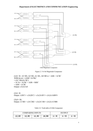
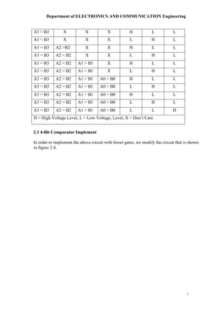
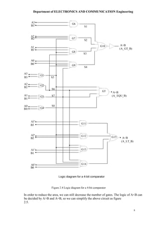
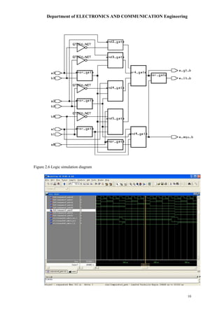
KEMBAR78
Digital 4-bit Comprator | PDF
Department of ELECTRONICS AND COMMUNICATION Engineering
Project Report for
Design of a 4-bit comparator
SSR
Department of ELECTRONICS AND COMMUNICATION Engineering
Abstract………………………………………………………………………2
1 Introduction…………………………………..…………………………….3
1.1Description of the project………………………………………………………………3
1.2 Performance Measures………………………………………………………………...3
1.3 Simulation……………………………………………………………………………..3
1.4 Layout…………………………………………………………………………………3
1.5 Design Kit and process technology ..…………………………………………………3
2 Logic design for 4-bit comparator…………………………………………4
2.1 logic design procedure………………………………………………………………...4
2.2 4-Bit Comparator……………………………………………………………………...6
2.3 4-Bit Comparator Implement………………………………………………………….7
2.4 Logic simulation……………………………………………………………………….9
3 Schematic level design and simulation…………………………………...12
3.1 XNOR circuit and simulation………………………………………………………...12
3.2 NOR circuit and simulation…………………………………………………………..14
3.3 SS1 circuit and simulation……………………………………………………………15 3.4
SS2 (4 Input AND) circuit and simulation…………………………………………...17
3.5 4-Bit comparator circuit and simulation……………………………………………...19
4 Layout and test……………………………………………………………21
4.1 Layout of XNOR……………………………………………………………………..21
4.2 Layout of NOR……………………………………………………………………….22
4.3 Layout of SS1………………………………………………………………………...24
4.4 Layout of SS2………………………………………………………………………...26
4.5 Layout of 4-Bit Comparator………………………………………………………….28
4.6 Conclusion……………………………………………………………………………30
5 Package……………………………………………………………………31
6 Summary………………………………………………………………….34 7
Reference………………………………………………………………….35
1
ABSTRACT
The goal of this project for the course COEN 6511 is to design a 4-bit
comparator, aiming to master the techniques of ASIC design.
The details of designing a 4-bit comparator are given in this report. It involves
the methodology, circuit implementation, schematic simulation, layout and
packaging.
We start from logic gate level, go up to the circuit level and then draw the
layout in the environment of CMOSIS5 in which the minimum drawing layout
size is 0.6μ. Finally we extract the layout as a symbol in the schematic for re-
Department of ELECTRONICS AND COMMUNICATION Engineering
simulation to obtain the results of the performance measure. In designing,
propagation delay, Area (A) and power are considered. All parameters of
circuit are decided and the circuit plot and waveform are produced, and we
would test and verify every part of the CMOS circuit developed by Cadence
development tools . The test results from simulation can meet the requirement.
It means that the logic design, schematic and layout are correct, and our
project can satisfy the requirements.
2
Department of ELECTRONICS AND COMMUNICATION Engineering
3
1. Introduction
1.1 Description of the project
The goal is the design of a 4-bit comparator. Input two 4-bit numbers A & B. Output is 3-bit
(A<B, A>B and A=B). We may use any comparison form and any logic form static,
dynamic, or any variation of these or within these families.
1.2 Performance Measures:
(1) Area (A), Time (T), Power (P), or AT2
are used as circuit performance. Initially we are
allowed to specify anyone of these factors to optimize our design.
(2) Testing: Choose an optimum test vector to test the design.
(3) Noise Margins: we are free to choose logic swing. The noise margins should be at least 10%
of the voltage swing.
(4) Rise and Fall times: All input signals and clocks have rise and fall times of less than 500
psec. The rise and fall times of the output signals (10% to 90%) should not exceed 1.5 nsec.
(5)Load capacitance: Each output bit of the comparator should have a 20 fF load.
1.3 Simulation:
Perform logic simulation, Circuit Simulation, and re-simulate the extracted circuit after
circuit extraction.
1.4 Layout:
Layout two gates of your design fully.
Perform DRC.
Extract the design and simulate it again and characterize these gates.
We are allowed to use any library cell from CADENCE . We are to perform DRC on the final
design, extract it and simulate it again to obtain performance measures. Then we are to place
and route the complete chip including all I/O drivers and PADs. Give a complete
specification for the circuit.
1.5 Design Kit and process technology
We develop our project by using the Schematic Editor and the Analog Artist simulation tools
available from Cadence package (CMOSIS5 design kit). The CMOSIS5 design kit is based
on the Hewlett-Packard CMOS14TB process. This is a high-speed, high-density 0.5 micron
CMOS process that features a 0.6 micron drawn gate length optimized for 3.3 V operation.
2 Logic design for 4-bit comparator
2.1 logic design procedure
Magnitude comparator is a combinational circuit that compares to numbers and determines
their relative magnitude. A comparator is shown as figure 2.1. The output of comparator is
usually 3 binary variables indicating:
A>B
A=B
Department of ELECTRONICS AND COMMUNICATION Engineering
4
A<B
For a 2-bit comparator (Figure 2.2), we have four inputs A1A0 and B1B0 and three outputs:
E (is 1 if two numbers are equal)
G (is 1 when A > B) and
L (is 1 when A < B)
E= A’1A’0B’1B’0 + A’1A0B’1B0 + A1A0B1B0 + A1A’0B1B’0 or E=(( A0 ⊕ B0) + ( A1
⊕ B1))’ G = A1B’1 + A0B’1B’0 + A1A0B’0
L= A’1B1 + A’1A’0B0 + A’0B1B0
Here we use simpler method to find E (called X) and G (called Y) and L (called Z) (1) A=B
if all Ai= Bi
Table 2.1
Ai Bi Xi
0 0 1
0 1 0
1 0 0
1 1 0
It means X0 = A0B0 + A’0B’0 and
X1= A1B1 + A’1B’1
If X0=1 and X1=1 then A0=B0 and A1=B1
Thus, if A=B then X0X1 = 1 it means
X= (A0B0 + A’0B’0)(A1B1 + A’1B’1) since (x ⊕ y)’ = (xy +x’y’)
Figure 2.1 1-bit comparator
Figure 2.2 2-bit comparator
If we use truth table and KMAP, the result is
Department of ELECTRONICS AND COMMUNICATION Engineering
5
X= ( A0⊕B0)’ ( A1⊕B1)’ = (( A0 ⊕ B0) + ( A1 ⊕ B1))’
It means for X we can NOR the result of two exclusive-OR gates.
(2) A>B means
Table 2.2
A1 B1 Y1
0 0 0
0 1 0
1 0 1
1 1 0
If A1=B1 (X1=1) then A0 should be 1 and B0 should be 0
Table 2.3
A0 B0 Y0
0 0 1
0 1 0
1 0 0
1 1 0
For A> B: A1 > B1 or
A1 =B1 and A0 > B0
It means Y= A1B’1 + X1A0B’0 should be 1 for A> B.
(3)For B>A: B1 > A1 or
A1=B1 and B0> A0
Z= A’1B1 + X1A’0B0
2.2 4-Bit Comparator
The procedure for binary numbers with more than 2 bits can also be found in the similar way.
The figure 2.3 shows the 4-bit magnitude comparator.
Input A=A3A2A1A0; B=B3B2B1B0
Department of ELECTRONICS AND COMMUNICATION Engineering
6
4-Bit Magnitude Comparator
Figure 2. 3 4- bit Magnitude Comparator
(1)A= B : A3=B3, A2=B2, A1=B1, A0=B0 xi = AiBi + Ai’Bi’
XOR-Invert = (AiBi’+Ai’Bi)’
= (Ai’+Bi)(Ai+Bi’)
= Ai’Ai + Ai’Bi’ + AiBi + BiBi’
= AiBi + Ai’Bi’
Output: x3x2x1x0
(2)A> B
Output: A3B’3 + x3A2B’2 + x3x2A1B’1+ x3x2x1A0B’0
(3)(A< B)
Output: A’3B3 + x3A’2B2 + x3x2A’1B1+ x3x2x1A’0B0
Table 2.4 Truth table of 4-Bit Comparator
COMPARING INPUTS OUTPUT
A3, B3 A2, B2 A1, B1 A0, B0 A > B A < B A = B
Department of ELECTRONICS AND COMMUNICATION Engineering
7
A3 > B3 X X X H L L
A3 < B3 X X X L H L
A3 = B3 A2 >B2 X X H L L
A3 = B3 A2 < B2 X X L H L
A3 = B3 A2 = B2 A1 > B1 X H L L
A3 = B3 A2 = B2 A1 < B1 X L H L
A3 = B3 A2 = B2 A1 = B1 A0 > B0 H L L
A3 = B3 A2 = B2 A1 = B1 A0 < B0 L H L
A3 = B3 A2 = B2 A1 = B1 A0 = B0 H L L
A3 = B3 A2 = B2 A1 = B1 A0 = B0 L H L
A3 = B3 A2 = B2 A1 = B1 A0 = B0 L L H
H = High Voltage Level, L = Low Voltage, Level, X = Don’t Care
2.3 4-Bit Comparator Implement
In order to implement the above circuit with fewer gates, we modify the circuit that is shown
in figure 2.4.
Department of ELECTRONICS AND COMMUNICATION Engineering
8
In order to reduce the area, we can still decrease the number of gates. The logic of A<B can
be decided by A>B and A=B, so we can simplify the above circuit as figure
2.5.
Department of ELECTRONICS AND COMMUNICATION Engineering
9
2-input NOR is used here to realize the function of A<B. The area of 2-input NOR is much
less than that of G11~G15. On the other hand, fewer gates means fewer power, so this
modification can greatly reduce the power dissipation. Therefore, the logic optimization is
completed.
Seeing from the above diagram, we can use 11 gates to implement the 4-Bit comparator
beside the inverters. The kind of gates includes XOR, AND, NOR. 4 gates of XOR are the
same. 5 gates of AND have different number of inputs, but the principle of layout is the same.
So does the NOR gate.
2.4 Logic simulation
In order to verify above design, we start to do logic simulation. The diagram is shown as
figure 2.6
Department of ELECTRONICS AND COMMUNICATION Engineering
10
Figure 2.6 Logic simulation diagram
Department of ELECTRONICS AND COMMUNICATION Engineering
11
Figure 2.7 Logic simulation result
From the simulation results (figure 2.7), we can get the conclusion that our logic analysis is
strictly right and then we begin to develop schematic level design.
3. Schematic level design and simulation
From the simplified logic diagram, we can see that the circuit include 4 XOR gates, 5 AND
gates with inputs from 2 to 5, 4 inputs and 2 inputs NOR and 5 inverters. In designing, we
select the time and the area as performance index for optimization. Although area is an
advantage for pseudo-Nmos, we will not adopt it after entirely thinking about td, tphl, tplh, area,
power dissipation and other performance parameters.
The time performance that we consider in this project includes propagation delay, Tr and Tf.
As shown in the simplified logic diagram, The SS1 block is more complicated than other
parts of circuit, so we choose propagation as the first index. We initially choose the size
Wp_eff=1.73Wn_eff. In other blocks we initially choose Wp_eff= 3Wn_eff to make Tr equal
to Tf.
In the diagram(figure 2.5), we can see that a 4 input NOR is used in the circuit. As we know,
NOR gates are costly. For the same performance, it results in increased area, power, delay,
output load capacitance (due to an increase in drain diffusion capacitance) and increase in
input capacitance presenting higher load to driver circuit. Normally we convert our circuit to
NAND and avoid use of large fan in NOR. But in this project, we still choose 2 inputs NOR
as for practice since its fan-in is only 2, and measure the performance to get the detailed data
with which we can compare the characteristics.
Here we display four parts of comparator schematic: XNOR, NOR, SS1, SS2, and measure
it after simulation.
3.1 XNOR circuit and simulation
XNOR schematic diagram is shown as figure 3.1
Department of ELECTRONICS AND COMMUNICATION Engineering
12
In the circuit, Wp=5.4microns Wn= 1.8microns, L= 0.6microns,
The simulation is done in the Synopsys simulation platform. The simulation
The test result is shown as table 3.1
Figure 3.1 Schematic of XNOR
waveform is shown as figure 3.2:
Figure 3.2 XNOR simulation waveform
Department of ELECTRONICS AND COMMUNICATION Engineering
13
table 3.1
TPLH TPHL Tr Tf Average power
106.7ps 113.5ps 179.3ps 107.0ps 3.755e-7w
3.2 NOR circuit and simulation
For each transistor in the circuit, L= 0.6microns, Wp=9.6microns, Wn=1.6micron The
simulation waveform is shown as figure 3.4:
2 inputs NOR schematic diagram is shown as figure 3.3
Figure 3.3 Schematic of NOR
Department of ELECTRONICS AND COMMUNICATION Engineering
14
own as table 3.2 table 3.2
TPLH TPHL Tr Tf Average power
72.3ps 57.01ps 115.0ps 26.5ps 1.636e-8w
3.3 SS1 circuit and simulation
The part of SS1 circuit includes G6,G7,G8,G9,G10 shown in the diagram. Its schematic
diagram is shown as figure 3.5:
Figure 3.4 NOR simulation waveform
Department of ELECTRONICS AND COMMUNICATION Engineering
15
In the circuit,Wp= 10.8microns, Wn=3.6microns, L= 0.6micron The simulation waveform
is shown as figure 3.6:
Figure 3.5 Schematic of SS1
Department of ELECTRONICS AND COMMUNICATION Engineering
16
The test result is shown as table 3.3
table 3.3
TPLH TPHL Tr Tf
Average power
689.4ps 257.6ps 1209.0ps 716.0ps 1.744e-5w
3.4 SS2 (4 Input AND) circuit and simulation
The schematic diagram of SS2 is shown as figure 3.7
Figure 3.6 SS1 simulation waveform
Department of ELECTRONICS AND COMMUNICATION Engineering
17
In the circuit, Wp=3.6microns, Wn=2.7micron, L=0.6micron
Figure 3.7 Schematic of SS2
The simulation waveform is shown as figure 3.8:
Figure 3.8 SS2 simulation waveform
Department of ELECTRONICS AND COMMUNICATION Engineering
18
The test result is shown as table 3.4
Table 3.4
TPLH TPHL Tr Tf
Average power
106.9p 111.0p 156.9p 146.2p 1.606e-07w
3.5 4-Bit comparator circuit and simulation
As we finished the above gates and circuit, we can integrate them as the whole 4-Bit
comparator. The following (figure 3.9) is the testbench schematic of 4-Bit comparator.
The simulation waveform is shown as figure 3.10
Figure 3.9 Testbench schematic of whole 4-bit comparator
Department of ELECTRONICS AND COMMUNICATION Engineering
19
The test result is shown as table 3.5:
Table 3.5
TPLH TPHL Tr Tf
Average power
992.33ps 1102.7ps 349.5ps 340.5ps 2.447e-06w
As shown in the waveform and table, our design can meet the project requirements, and then
we can start to develop the layout.
4 Layout and test
Having finished the schematic level design and simulation successfully, we can do the layout
and extract it to the schematic for test.
Although we only need to layout 2 gates in this project and can use any standard library, we
plan to layout all the gates by ourselves. The first reason is that the standard library maybe
cannot meet our requirement. In most situations, we need to adjust the parameter of the
transistor to meet the requirements of the project. For example, we need to adjust the Wp/Wn,
Spacing, width to obtain the desired characteristics. However, the layout from standard
library is difficult to adjust to meet our requirements. In addition, more layouts by hand can
help us to improve the skills, and it is one of the purposes of the project we believe.
Figure 3.10 4-bit comparator simulation waveform
Department of ELECTRONICS AND COMMUNICATION Engineering
20
4.1 Layout of XNOR
The layout of XNOR is shown as figure 4.1
We extract it as a symbol and test it in the test schematic. The simulation waveform is shown
as figure 4.2:
Figure 4.1 the layout of XNOR
Department of ELECTRONICS AND COMMUNICATION Engineering
21
The test result is shown as table 4.1
Table 4.1
TPLH TPHL Tr Tf NML NMH Aaverage
power
Area
(um2
)
230.0ps 305.2ps 349.6ps 271.1ps 0.93v 1.80v 1.812e-06w 19.8*16.4
4.2 Layout of NOR
The layout of AND is shown as figure 4.3.
Figure 4.2 Extracted XNOR simulation waveform
Department of ELECTRONICS AND COMMUNICATION Engineering
22
We extract it as a symbol and test it in the test schematic. The simulation waveform is
Figure 4.3 the layout of NOR
shown as figure 4.4:
Figure 4.4 Extracted NOR simulation waveform
Department of ELECTRONICS AND COMMUNICATION Engineering
23
The test result is shown as table 4.2:
Table 4.2
TPLH TPHL Tr Tf NML NMH Average
power
Area
(um2
)
103.4ps 80.63ps 166.3ps 96.6ps 0.82v 1.76v 1.14e-06w 47.7*32.4
4.3 Layout of SS1
SS1 is the most complicated part in the project. Euler network of SS1 is shown as below
according which we can minimize the area of layout.
Figure 4.5 Euler network of SS1
The layout of SS1 is shown as figure 4.6:
3 3A B
22A B
33A B
11A B
22A B
33A B
0A
0A
1A
1A
2B 2A
3A
3B
33A B
22A B
11A B
2 2A B
33A B
2A
33A B
3B
1B
0B3A 2A
1A
Department of ELECTRONICS AND COMMUNICATION Engineering
24
Figure 4.6 the layout of SS1
We extract it as a symbol and test it in the test schematic. The simulation waveform is shown
as figure 4.7:
Department of ELECTRONICS AND COMMUNICATION Engineering
25
The test result is shown as table 4.3:
Table 4.3
TPLH TPHL Tr Tf NML NMH Average
power
Area
(um2
)
712.4ps 593.8ps 1130.3ps 1041.2ps 0.98v 1.86v 4.3e-06w 47.7*32.4
4.4 Layout of SS2
The layout of SS2 is shown as figure 4.8:
Figure 4.7 Extracted SS1 simulation waveform
Department of ELECTRONICS AND COMMUNICATION Engineering
26
We extract it as a symbol and test it in the test schematic. The simulation waveform is shown
as figure 4.9:
Figure 4.8 the layout of SS1
Department of ELECTRONICS AND COMMUNICATION Engineering
27
The test result is shown as table 4.4:
Table 4.4
TPLH TPHL Tr Tf NML NMH average
power
Area (um2
)
212.3ps 195.2ps 265.5ps 164.6ps 0.85v 1.70v 1.77e-06w 16.5*16.7
4.5 Layout of 4-Bit Comparator
The layout of 4-Bit comparator is shown as figure 4.10:
Figure 4.9 Extracted SS2 simulation waveform
Department of ELECTRONICS AND COMMUNICATION Engineering
28
We extract it as a symbol and test it in the test schematic. The simulation waveform is
Figure 4.10 the layout of whole 4-bit comparator
shown as figure 4.9:
Department of ELECTRONICS AND COMMUNICATION Engineering
29
m above, the objective test results can be shown as table 4.5: Table4.5
TPLH TPHL Tr Tf NML NMH Average
power
Area (um2
)
983.61ps 1162.2ps 314.3ps 363.1ps 0.88v 1.82v 7.842e-06w 114.8*124.3
4.6 Conclusion
From the layouts and tables, we can see that our design can satisfy the requirements. Area is
a very important index in ASIC design. As for us, it is first time to layout gates and whole
circuit. One of the experiences is that the minimum area of each gate does not mean the
minimum area of whole circuit can be reached. For integration of gates, we also need to
consider the direction of signal and its connection. Unreasonable layout of signal direction
will waste much area when we integrate gates to a whole layout.
5 Packaging
In our chip, there are 8 input pads : A0-A3,B0-B3. We use the pads of PADINC in hells
library, then make the connection with the correspondent input in the circuit using metal1 dg
layer. There are 3 output pads: G(A>B), E(A=B), L(A<B); The other two pads is VDD and
VSS. The PAD connections are shown as figure 5.1:
Figure 4.9 Extracted 4-bit comparator simulation waveform
Department of ELECTRONICS AND COMMUNICATION Engineering
30
Figure 5.1 PAD connection
Figure 5.2 is the whole circuit layout with I/O drivers.
Department of ELECTRONICS AND COMMUNICATION Engineering
31
Figure 5.2 the whole circuit layout
The Pins are defined as figure 5.3 and table 5.1
Department of ELECTRONICS AND COMMUNICATION Engineering
32
Table 5.1
Pin
Number
Signal Input Output VDD VSS(GND)
1 A0 √
2 B0 √
3 A1 √
4 B1 √
5 A2 √
6 B2 √
7 VSS √
8 A3 √
9 B3 √
10 IDLE
11 L √
12 E √
13 G √
14 VDD √
Department of ELECTRONICS AND COMMUNICATION Engineering
33
6 Summary
From the logic design, schematic level design and simulation, layout, re-simulation and
packaging, it is clear that the logic design is correct and simple to implement. According to
the basic principles of CMOS circuit design, the appropriate parameters can be decided after
several attempts to get better performance during the course of the circuit schematic design.
Guided by the schematic design and CMOSIS5 design Rules, the layout can be obtained after
the rational arrangement of all parts of circuit. And re-simulating the extracted circuit after
layout extraction, we attained the values of td, tplh, tphl, area, power dissipation and other
performance parameters closer to the real application.
The difference between the results from circuit design simulation and layout simulation
provides us specific clues for improving the layout and at the same time, we must see that the
layout is closer to real IC. For the practical application, some effects will be unavoidable,
which is different from the circuit design simulation. Ordinarily, the time performance
parameters from layout simulation are always greater than those from circuit design
simulation. Another experience for layout is that the locally reasonable arrangement is not
equal to the wholly reasonable arrangement and the wholly reasonable arrangement will be
more significant for the design of large-scaled IC design.
In general, we have learned many CMOS digital integrated circuits analysis methods and
design techniques.

Digital 4-bit Comprator

  • 1.
    Department of ELECTRONICSAND COMMUNICATION Engineering Project Report for Design of a 4-bit comparator SSR
  • 2.
    Department of ELECTRONICSAND COMMUNICATION Engineering Abstract………………………………………………………………………2 1 Introduction…………………………………..…………………………….3 1.1Description of the project………………………………………………………………3 1.2 Performance Measures………………………………………………………………...3 1.3 Simulation……………………………………………………………………………..3 1.4 Layout…………………………………………………………………………………3 1.5 Design Kit and process technology ..…………………………………………………3 2 Logic design for 4-bit comparator…………………………………………4 2.1 logic design procedure………………………………………………………………...4 2.2 4-Bit Comparator……………………………………………………………………...6 2.3 4-Bit Comparator Implement………………………………………………………….7 2.4 Logic simulation……………………………………………………………………….9 3 Schematic level design and simulation…………………………………...12 3.1 XNOR circuit and simulation………………………………………………………...12 3.2 NOR circuit and simulation…………………………………………………………..14 3.3 SS1 circuit and simulation……………………………………………………………15 3.4 SS2 (4 Input AND) circuit and simulation…………………………………………...17 3.5 4-Bit comparator circuit and simulation……………………………………………...19 4 Layout and test……………………………………………………………21 4.1 Layout of XNOR……………………………………………………………………..21 4.2 Layout of NOR……………………………………………………………………….22 4.3 Layout of SS1………………………………………………………………………...24 4.4 Layout of SS2………………………………………………………………………...26 4.5 Layout of 4-Bit Comparator………………………………………………………….28 4.6 Conclusion……………………………………………………………………………30 5 Package……………………………………………………………………31 6 Summary………………………………………………………………….34 7 Reference………………………………………………………………….35 1 ABSTRACT The goal of this project for the course COEN 6511 is to design a 4-bit comparator, aiming to master the techniques of ASIC design. The details of designing a 4-bit comparator are given in this report. It involves the methodology, circuit implementation, schematic simulation, layout and packaging. We start from logic gate level, go up to the circuit level and then draw the layout in the environment of CMOSIS5 in which the minimum drawing layout size is 0.6μ. Finally we extract the layout as a symbol in the schematic for re-
  • 3.
    Department of ELECTRONICSAND COMMUNICATION Engineering simulation to obtain the results of the performance measure. In designing, propagation delay, Area (A) and power are considered. All parameters of circuit are decided and the circuit plot and waveform are produced, and we would test and verify every part of the CMOS circuit developed by Cadence development tools . The test results from simulation can meet the requirement. It means that the logic design, schematic and layout are correct, and our project can satisfy the requirements. 2
  • 4.
    Department of ELECTRONICSAND COMMUNICATION Engineering 3 1. Introduction 1.1 Description of the project The goal is the design of a 4-bit comparator. Input two 4-bit numbers A & B. Output is 3-bit (A<B, A>B and A=B). We may use any comparison form and any logic form static, dynamic, or any variation of these or within these families. 1.2 Performance Measures: (1) Area (A), Time (T), Power (P), or AT2 are used as circuit performance. Initially we are allowed to specify anyone of these factors to optimize our design. (2) Testing: Choose an optimum test vector to test the design. (3) Noise Margins: we are free to choose logic swing. The noise margins should be at least 10% of the voltage swing. (4) Rise and Fall times: All input signals and clocks have rise and fall times of less than 500 psec. The rise and fall times of the output signals (10% to 90%) should not exceed 1.5 nsec. (5)Load capacitance: Each output bit of the comparator should have a 20 fF load. 1.3 Simulation: Perform logic simulation, Circuit Simulation, and re-simulate the extracted circuit after circuit extraction. 1.4 Layout: Layout two gates of your design fully. Perform DRC. Extract the design and simulate it again and characterize these gates. We are allowed to use any library cell from CADENCE . We are to perform DRC on the final design, extract it and simulate it again to obtain performance measures. Then we are to place and route the complete chip including all I/O drivers and PADs. Give a complete specification for the circuit. 1.5 Design Kit and process technology We develop our project by using the Schematic Editor and the Analog Artist simulation tools available from Cadence package (CMOSIS5 design kit). The CMOSIS5 design kit is based on the Hewlett-Packard CMOS14TB process. This is a high-speed, high-density 0.5 micron CMOS process that features a 0.6 micron drawn gate length optimized for 3.3 V operation. 2 Logic design for 4-bit comparator 2.1 logic design procedure Magnitude comparator is a combinational circuit that compares to numbers and determines their relative magnitude. A comparator is shown as figure 2.1. The output of comparator is usually 3 binary variables indicating: A>B A=B
  • 5.
    Department of ELECTRONICSAND COMMUNICATION Engineering 4 A<B For a 2-bit comparator (Figure 2.2), we have four inputs A1A0 and B1B0 and three outputs: E (is 1 if two numbers are equal) G (is 1 when A > B) and L (is 1 when A < B) E= A’1A’0B’1B’0 + A’1A0B’1B0 + A1A0B1B0 + A1A’0B1B’0 or E=(( A0 ⊕ B0) + ( A1 ⊕ B1))’ G = A1B’1 + A0B’1B’0 + A1A0B’0 L= A’1B1 + A’1A’0B0 + A’0B1B0 Here we use simpler method to find E (called X) and G (called Y) and L (called Z) (1) A=B if all Ai= Bi Table 2.1 Ai Bi Xi 0 0 1 0 1 0 1 0 0 1 1 0 It means X0 = A0B0 + A’0B’0 and X1= A1B1 + A’1B’1 If X0=1 and X1=1 then A0=B0 and A1=B1 Thus, if A=B then X0X1 = 1 it means X= (A0B0 + A’0B’0)(A1B1 + A’1B’1) since (x ⊕ y)’ = (xy +x’y’) Figure 2.1 1-bit comparator Figure 2.2 2-bit comparator If we use truth table and KMAP, the result is
  • 6.
    Department of ELECTRONICSAND COMMUNICATION Engineering 5 X= ( A0⊕B0)’ ( A1⊕B1)’ = (( A0 ⊕ B0) + ( A1 ⊕ B1))’ It means for X we can NOR the result of two exclusive-OR gates. (2) A>B means Table 2.2 A1 B1 Y1 0 0 0 0 1 0 1 0 1 1 1 0 If A1=B1 (X1=1) then A0 should be 1 and B0 should be 0 Table 2.3 A0 B0 Y0 0 0 1 0 1 0 1 0 0 1 1 0 For A> B: A1 > B1 or A1 =B1 and A0 > B0 It means Y= A1B’1 + X1A0B’0 should be 1 for A> B. (3)For B>A: B1 > A1 or A1=B1 and B0> A0 Z= A’1B1 + X1A’0B0 2.2 4-Bit Comparator The procedure for binary numbers with more than 2 bits can also be found in the similar way. The figure 2.3 shows the 4-bit magnitude comparator. Input A=A3A2A1A0; B=B3B2B1B0
  • 7.
    Department of ELECTRONICSAND COMMUNICATION Engineering 6 4-Bit Magnitude Comparator Figure 2. 3 4- bit Magnitude Comparator (1)A= B : A3=B3, A2=B2, A1=B1, A0=B0 xi = AiBi + Ai’Bi’ XOR-Invert = (AiBi’+Ai’Bi)’ = (Ai’+Bi)(Ai+Bi’) = Ai’Ai + Ai’Bi’ + AiBi + BiBi’ = AiBi + Ai’Bi’ Output: x3x2x1x0 (2)A> B Output: A3B’3 + x3A2B’2 + x3x2A1B’1+ x3x2x1A0B’0 (3)(A< B) Output: A’3B3 + x3A’2B2 + x3x2A’1B1+ x3x2x1A’0B0 Table 2.4 Truth table of 4-Bit Comparator COMPARING INPUTS OUTPUT A3, B3 A2, B2 A1, B1 A0, B0 A > B A < B A = B
  • 8.
    Department of ELECTRONICSAND COMMUNICATION Engineering 7 A3 > B3 X X X H L L A3 < B3 X X X L H L A3 = B3 A2 >B2 X X H L L A3 = B3 A2 < B2 X X L H L A3 = B3 A2 = B2 A1 > B1 X H L L A3 = B3 A2 = B2 A1 < B1 X L H L A3 = B3 A2 = B2 A1 = B1 A0 > B0 H L L A3 = B3 A2 = B2 A1 = B1 A0 < B0 L H L A3 = B3 A2 = B2 A1 = B1 A0 = B0 H L L A3 = B3 A2 = B2 A1 = B1 A0 = B0 L H L A3 = B3 A2 = B2 A1 = B1 A0 = B0 L L H H = High Voltage Level, L = Low Voltage, Level, X = Don’t Care 2.3 4-Bit Comparator Implement In order to implement the above circuit with fewer gates, we modify the circuit that is shown in figure 2.4.
  • 9.
    Department of ELECTRONICSAND COMMUNICATION Engineering 8 In order to reduce the area, we can still decrease the number of gates. The logic of A<B can be decided by A>B and A=B, so we can simplify the above circuit as figure 2.5.
  • 10.
    Department of ELECTRONICSAND COMMUNICATION Engineering 9 2-input NOR is used here to realize the function of A<B. The area of 2-input NOR is much less than that of G11~G15. On the other hand, fewer gates means fewer power, so this modification can greatly reduce the power dissipation. Therefore, the logic optimization is completed. Seeing from the above diagram, we can use 11 gates to implement the 4-Bit comparator beside the inverters. The kind of gates includes XOR, AND, NOR. 4 gates of XOR are the same. 5 gates of AND have different number of inputs, but the principle of layout is the same. So does the NOR gate. 2.4 Logic simulation In order to verify above design, we start to do logic simulation. The diagram is shown as figure 2.6
  • 11.
    Department of ELECTRONICSAND COMMUNICATION Engineering 10 Figure 2.6 Logic simulation diagram
  • 12.
    Department of ELECTRONICSAND COMMUNICATION Engineering 11 Figure 2.7 Logic simulation result From the simulation results (figure 2.7), we can get the conclusion that our logic analysis is strictly right and then we begin to develop schematic level design. 3. Schematic level design and simulation From the simplified logic diagram, we can see that the circuit include 4 XOR gates, 5 AND gates with inputs from 2 to 5, 4 inputs and 2 inputs NOR and 5 inverters. In designing, we select the time and the area as performance index for optimization. Although area is an advantage for pseudo-Nmos, we will not adopt it after entirely thinking about td, tphl, tplh, area, power dissipation and other performance parameters. The time performance that we consider in this project includes propagation delay, Tr and Tf. As shown in the simplified logic diagram, The SS1 block is more complicated than other parts of circuit, so we choose propagation as the first index. We initially choose the size Wp_eff=1.73Wn_eff. In other blocks we initially choose Wp_eff= 3Wn_eff to make Tr equal to Tf. In the diagram(figure 2.5), we can see that a 4 input NOR is used in the circuit. As we know, NOR gates are costly. For the same performance, it results in increased area, power, delay, output load capacitance (due to an increase in drain diffusion capacitance) and increase in input capacitance presenting higher load to driver circuit. Normally we convert our circuit to NAND and avoid use of large fan in NOR. But in this project, we still choose 2 inputs NOR as for practice since its fan-in is only 2, and measure the performance to get the detailed data with which we can compare the characteristics. Here we display four parts of comparator schematic: XNOR, NOR, SS1, SS2, and measure it after simulation. 3.1 XNOR circuit and simulation XNOR schematic diagram is shown as figure 3.1
  • 13.
    Department of ELECTRONICSAND COMMUNICATION Engineering 12 In the circuit, Wp=5.4microns Wn= 1.8microns, L= 0.6microns, The simulation is done in the Synopsys simulation platform. The simulation The test result is shown as table 3.1 Figure 3.1 Schematic of XNOR waveform is shown as figure 3.2: Figure 3.2 XNOR simulation waveform
  • 14.
    Department of ELECTRONICSAND COMMUNICATION Engineering 13 table 3.1 TPLH TPHL Tr Tf Average power 106.7ps 113.5ps 179.3ps 107.0ps 3.755e-7w 3.2 NOR circuit and simulation For each transistor in the circuit, L= 0.6microns, Wp=9.6microns, Wn=1.6micron The simulation waveform is shown as figure 3.4: 2 inputs NOR schematic diagram is shown as figure 3.3 Figure 3.3 Schematic of NOR
  • 15.
    Department of ELECTRONICSAND COMMUNICATION Engineering 14 own as table 3.2 table 3.2 TPLH TPHL Tr Tf Average power 72.3ps 57.01ps 115.0ps 26.5ps 1.636e-8w 3.3 SS1 circuit and simulation The part of SS1 circuit includes G6,G7,G8,G9,G10 shown in the diagram. Its schematic diagram is shown as figure 3.5: Figure 3.4 NOR simulation waveform
  • 16.
    Department of ELECTRONICSAND COMMUNICATION Engineering 15 In the circuit,Wp= 10.8microns, Wn=3.6microns, L= 0.6micron The simulation waveform is shown as figure 3.6: Figure 3.5 Schematic of SS1
  • 17.
    Department of ELECTRONICSAND COMMUNICATION Engineering 16 The test result is shown as table 3.3 table 3.3 TPLH TPHL Tr Tf Average power 689.4ps 257.6ps 1209.0ps 716.0ps 1.744e-5w 3.4 SS2 (4 Input AND) circuit and simulation The schematic diagram of SS2 is shown as figure 3.7 Figure 3.6 SS1 simulation waveform
  • 18.
    Department of ELECTRONICSAND COMMUNICATION Engineering 17 In the circuit, Wp=3.6microns, Wn=2.7micron, L=0.6micron Figure 3.7 Schematic of SS2 The simulation waveform is shown as figure 3.8: Figure 3.8 SS2 simulation waveform
  • 19.
    Department of ELECTRONICSAND COMMUNICATION Engineering 18 The test result is shown as table 3.4 Table 3.4 TPLH TPHL Tr Tf Average power 106.9p 111.0p 156.9p 146.2p 1.606e-07w 3.5 4-Bit comparator circuit and simulation As we finished the above gates and circuit, we can integrate them as the whole 4-Bit comparator. The following (figure 3.9) is the testbench schematic of 4-Bit comparator. The simulation waveform is shown as figure 3.10 Figure 3.9 Testbench schematic of whole 4-bit comparator
  • 20.
    Department of ELECTRONICSAND COMMUNICATION Engineering 19 The test result is shown as table 3.5: Table 3.5 TPLH TPHL Tr Tf Average power 992.33ps 1102.7ps 349.5ps 340.5ps 2.447e-06w As shown in the waveform and table, our design can meet the project requirements, and then we can start to develop the layout. 4 Layout and test Having finished the schematic level design and simulation successfully, we can do the layout and extract it to the schematic for test. Although we only need to layout 2 gates in this project and can use any standard library, we plan to layout all the gates by ourselves. The first reason is that the standard library maybe cannot meet our requirement. In most situations, we need to adjust the parameter of the transistor to meet the requirements of the project. For example, we need to adjust the Wp/Wn, Spacing, width to obtain the desired characteristics. However, the layout from standard library is difficult to adjust to meet our requirements. In addition, more layouts by hand can help us to improve the skills, and it is one of the purposes of the project we believe. Figure 3.10 4-bit comparator simulation waveform
  • 21.
    Department of ELECTRONICSAND COMMUNICATION Engineering 20 4.1 Layout of XNOR The layout of XNOR is shown as figure 4.1 We extract it as a symbol and test it in the test schematic. The simulation waveform is shown as figure 4.2: Figure 4.1 the layout of XNOR
  • 22.
    Department of ELECTRONICSAND COMMUNICATION Engineering 21 The test result is shown as table 4.1 Table 4.1 TPLH TPHL Tr Tf NML NMH Aaverage power Area (um2 ) 230.0ps 305.2ps 349.6ps 271.1ps 0.93v 1.80v 1.812e-06w 19.8*16.4 4.2 Layout of NOR The layout of AND is shown as figure 4.3. Figure 4.2 Extracted XNOR simulation waveform
  • 23.
    Department of ELECTRONICSAND COMMUNICATION Engineering 22 We extract it as a symbol and test it in the test schematic. The simulation waveform is Figure 4.3 the layout of NOR shown as figure 4.4: Figure 4.4 Extracted NOR simulation waveform
  • 24.
    Department of ELECTRONICSAND COMMUNICATION Engineering 23 The test result is shown as table 4.2: Table 4.2 TPLH TPHL Tr Tf NML NMH Average power Area (um2 ) 103.4ps 80.63ps 166.3ps 96.6ps 0.82v 1.76v 1.14e-06w 47.7*32.4 4.3 Layout of SS1 SS1 is the most complicated part in the project. Euler network of SS1 is shown as below according which we can minimize the area of layout. Figure 4.5 Euler network of SS1 The layout of SS1 is shown as figure 4.6: 3 3A B 22A B 33A B 11A B 22A B 33A B 0A 0A 1A 1A 2B 2A 3A 3B 33A B 22A B 11A B 2 2A B 33A B 2A 33A B 3B 1B 0B3A 2A 1A
  • 25.
    Department of ELECTRONICSAND COMMUNICATION Engineering 24 Figure 4.6 the layout of SS1 We extract it as a symbol and test it in the test schematic. The simulation waveform is shown as figure 4.7:
  • 26.
    Department of ELECTRONICSAND COMMUNICATION Engineering 25 The test result is shown as table 4.3: Table 4.3 TPLH TPHL Tr Tf NML NMH Average power Area (um2 ) 712.4ps 593.8ps 1130.3ps 1041.2ps 0.98v 1.86v 4.3e-06w 47.7*32.4 4.4 Layout of SS2 The layout of SS2 is shown as figure 4.8: Figure 4.7 Extracted SS1 simulation waveform
  • 27.
    Department of ELECTRONICSAND COMMUNICATION Engineering 26 We extract it as a symbol and test it in the test schematic. The simulation waveform is shown as figure 4.9: Figure 4.8 the layout of SS1
  • 28.
    Department of ELECTRONICSAND COMMUNICATION Engineering 27 The test result is shown as table 4.4: Table 4.4 TPLH TPHL Tr Tf NML NMH average power Area (um2 ) 212.3ps 195.2ps 265.5ps 164.6ps 0.85v 1.70v 1.77e-06w 16.5*16.7 4.5 Layout of 4-Bit Comparator The layout of 4-Bit comparator is shown as figure 4.10: Figure 4.9 Extracted SS2 simulation waveform
  • 29.
    Department of ELECTRONICSAND COMMUNICATION Engineering 28 We extract it as a symbol and test it in the test schematic. The simulation waveform is Figure 4.10 the layout of whole 4-bit comparator shown as figure 4.9:
  • 30.
    Department of ELECTRONICSAND COMMUNICATION Engineering 29 m above, the objective test results can be shown as table 4.5: Table4.5 TPLH TPHL Tr Tf NML NMH Average power Area (um2 ) 983.61ps 1162.2ps 314.3ps 363.1ps 0.88v 1.82v 7.842e-06w 114.8*124.3 4.6 Conclusion From the layouts and tables, we can see that our design can satisfy the requirements. Area is a very important index in ASIC design. As for us, it is first time to layout gates and whole circuit. One of the experiences is that the minimum area of each gate does not mean the minimum area of whole circuit can be reached. For integration of gates, we also need to consider the direction of signal and its connection. Unreasonable layout of signal direction will waste much area when we integrate gates to a whole layout. 5 Packaging In our chip, there are 8 input pads : A0-A3,B0-B3. We use the pads of PADINC in hells library, then make the connection with the correspondent input in the circuit using metal1 dg layer. There are 3 output pads: G(A>B), E(A=B), L(A<B); The other two pads is VDD and VSS. The PAD connections are shown as figure 5.1: Figure 4.9 Extracted 4-bit comparator simulation waveform
  • 31.
    Department of ELECTRONICSAND COMMUNICATION Engineering 30 Figure 5.1 PAD connection Figure 5.2 is the whole circuit layout with I/O drivers.
  • 32.
    Department of ELECTRONICSAND COMMUNICATION Engineering 31 Figure 5.2 the whole circuit layout The Pins are defined as figure 5.3 and table 5.1
  • 33.
    Department of ELECTRONICSAND COMMUNICATION Engineering 32 Table 5.1 Pin Number Signal Input Output VDD VSS(GND) 1 A0 √ 2 B0 √ 3 A1 √ 4 B1 √ 5 A2 √ 6 B2 √ 7 VSS √ 8 A3 √ 9 B3 √ 10 IDLE 11 L √ 12 E √ 13 G √ 14 VDD √
  • 34.
    Department of ELECTRONICSAND COMMUNICATION Engineering 33 6 Summary From the logic design, schematic level design and simulation, layout, re-simulation and packaging, it is clear that the logic design is correct and simple to implement. According to the basic principles of CMOS circuit design, the appropriate parameters can be decided after several attempts to get better performance during the course of the circuit schematic design. Guided by the schematic design and CMOSIS5 design Rules, the layout can be obtained after the rational arrangement of all parts of circuit. And re-simulating the extracted circuit after layout extraction, we attained the values of td, tplh, tphl, area, power dissipation and other performance parameters closer to the real application. The difference between the results from circuit design simulation and layout simulation provides us specific clues for improving the layout and at the same time, we must see that the layout is closer to real IC. For the practical application, some effects will be unavoidable, which is different from the circuit design simulation. Ordinarily, the time performance parameters from layout simulation are always greater than those from circuit design simulation. Another experience for layout is that the locally reasonable arrangement is not equal to the wholly reasonable arrangement and the wholly reasonable arrangement will be more significant for the design of large-scaled IC design. In general, we have learned many CMOS digital integrated circuits analysis methods and design techniques.