Digital logic and computer design with Unit 2 topics
1.
09/25/2025 UNIT-IV
Digital Logicand Computer Architecture
B23DA0101-Academic Year 2024-25 Odd Semester
BCA, School of CSA
P ro f. P a d m a v a t h i R
A s s i s t a n t P ro f e s s o r
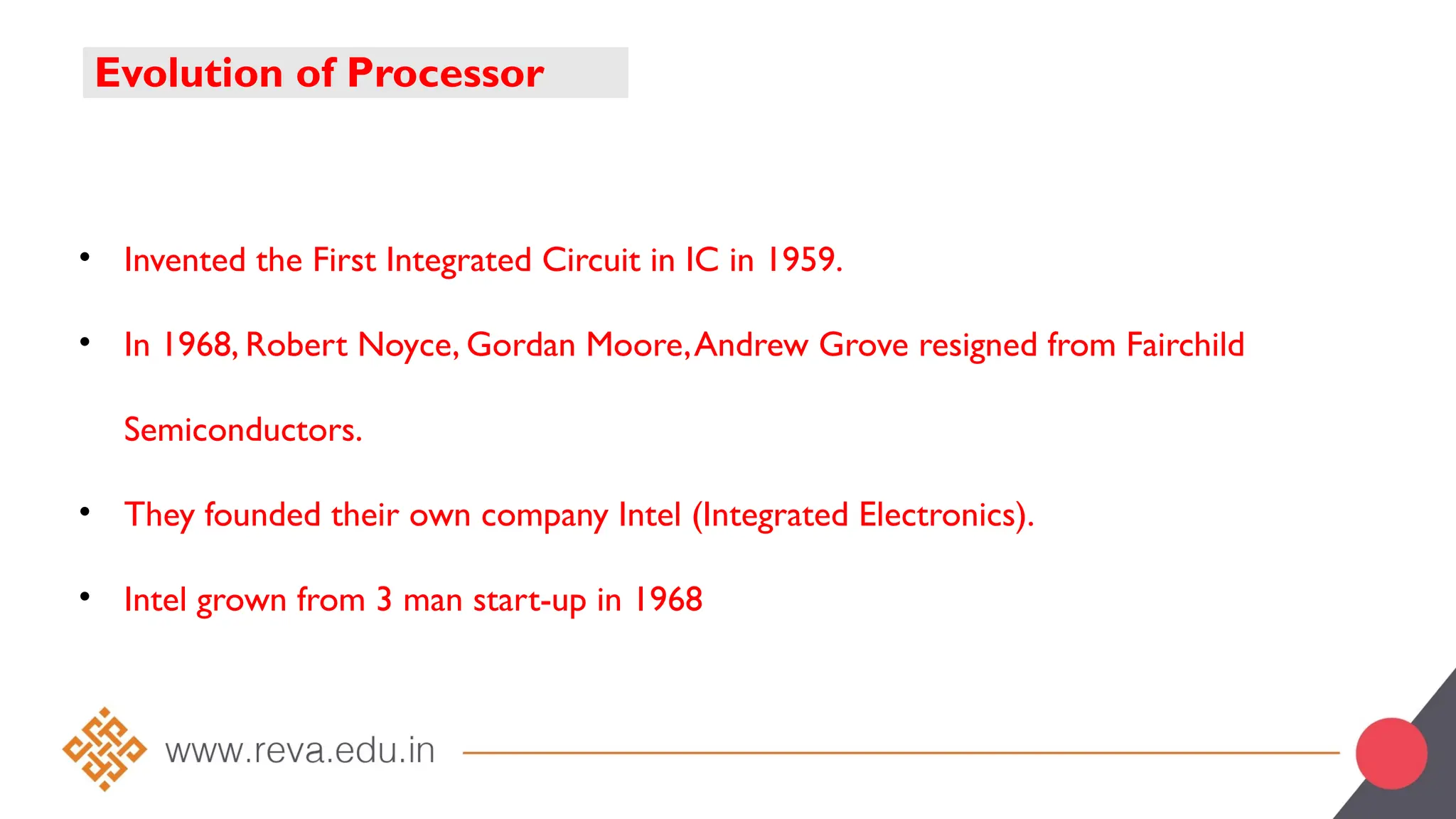
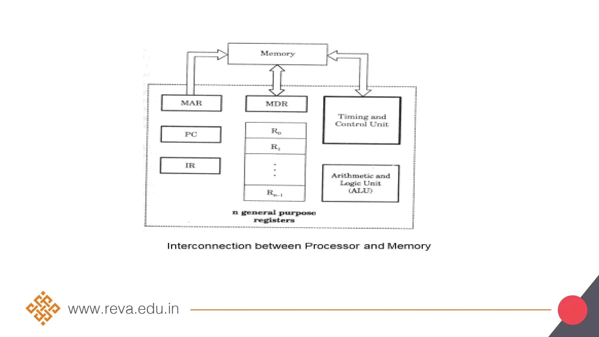
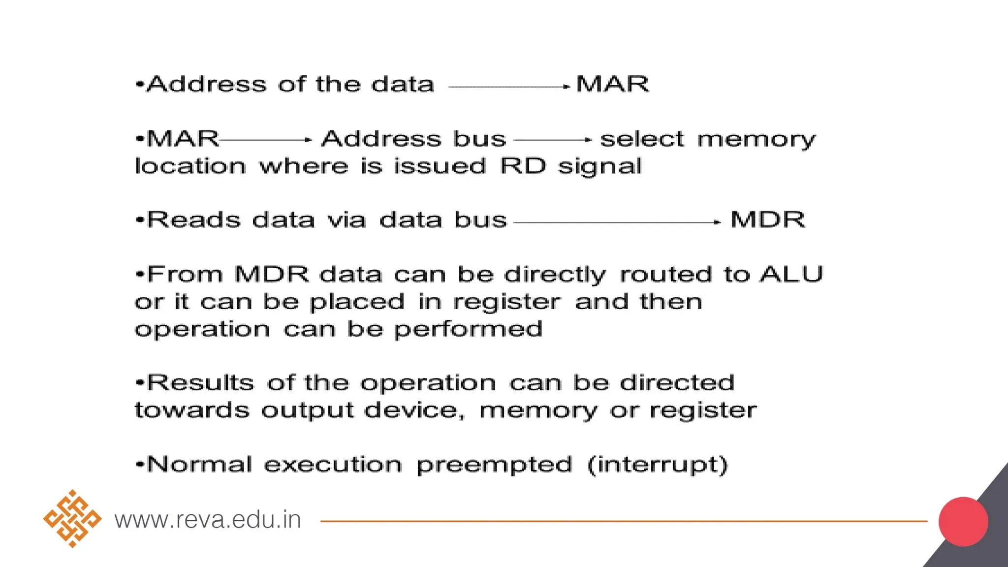
Evolution of Processor
•Invented the First Integrated Circuit in IC in 1959.
• In 1968, Robert Noyce, Gordan Moore,Andrew Grove resigned from Fairchild
Semiconductors.
• They founded their own company Intel (Integrated Electronics).
• Intel grown from 3 man start-up in 1968
4.
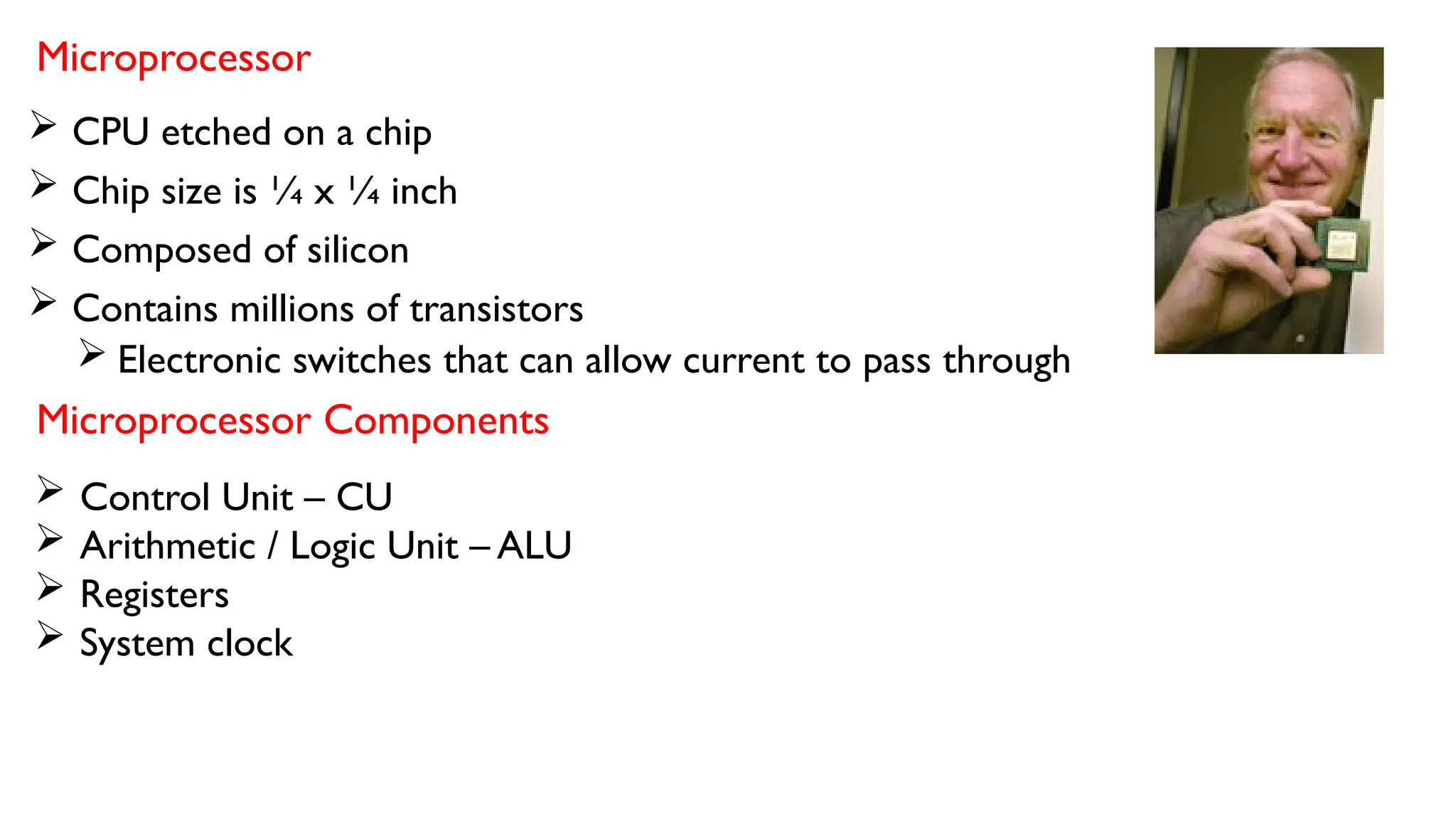
Microprocessor
CPU etchedon a chip
Chip size is ¼ x ¼ inch
Composed of silicon
Contains millions of transistors
Electronic switches that can allow current to pass through
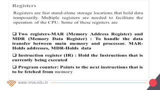
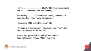
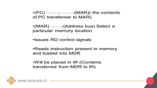
Microprocessor Components
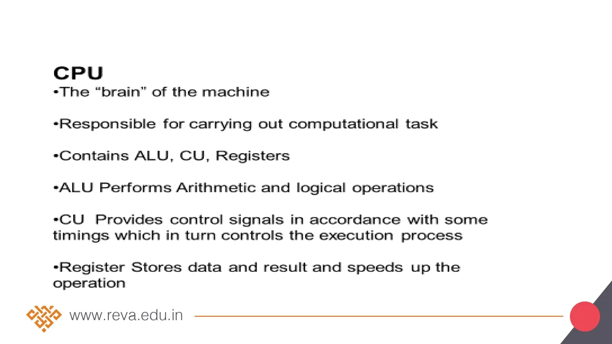
Control Unit – CU
Arithmetic / Logic Unit – ALU
Registers
System clock
5.
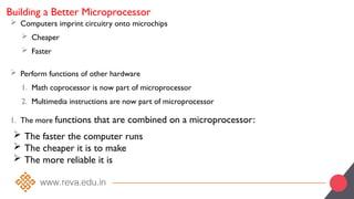
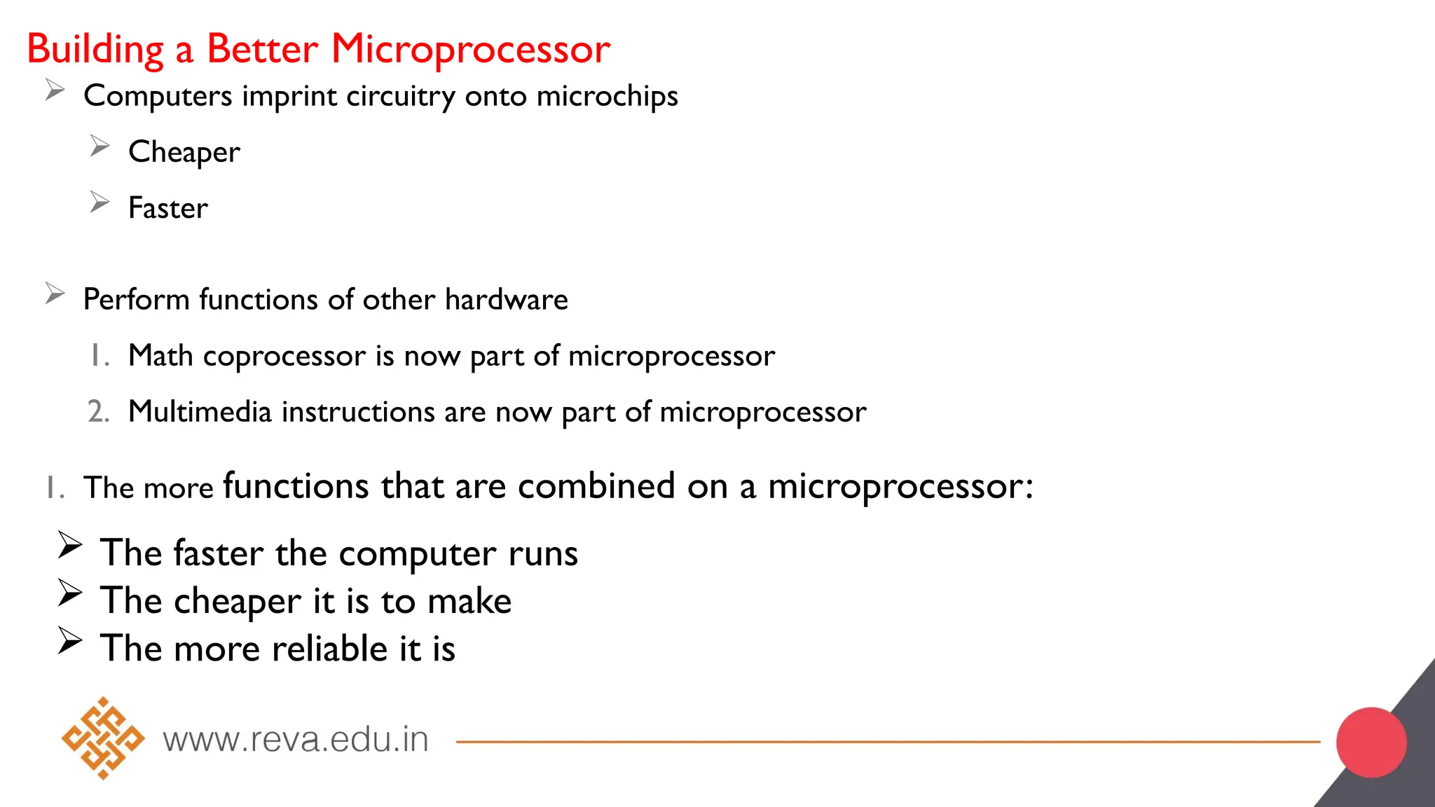
Building a BetterMicroprocessor
Computers imprint circuitry onto microchips
Cheaper
Faster
Perform functions of other hardware
1. Math coprocessor is now part of microprocessor
2. Multimedia instructions are now part of microprocessor
1. The more functions that are combined on a microprocessor:
The faster the computer runs
The cheaper it is to make
The more reliable it is
6.
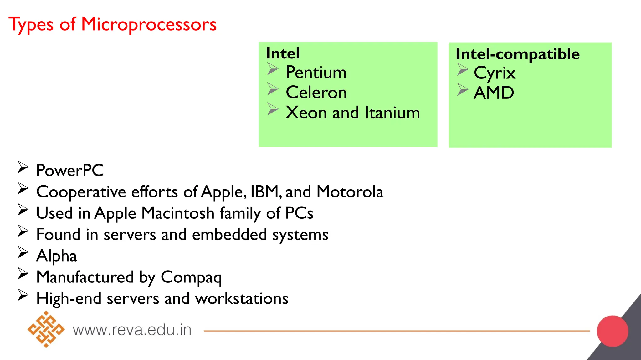
Types of Microprocessors
Intel
Pentium
Celeron
Xeon and Itanium
Intel-compatible
Cyrix
AMD
PowerPC
Cooperative efforts of Apple, IBM, and Motorola
Used in Apple Macintosh family of PCs
Found in servers and embedded systems
Alpha
Manufactured by Compaq
High-end servers and workstations
7.
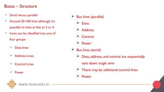
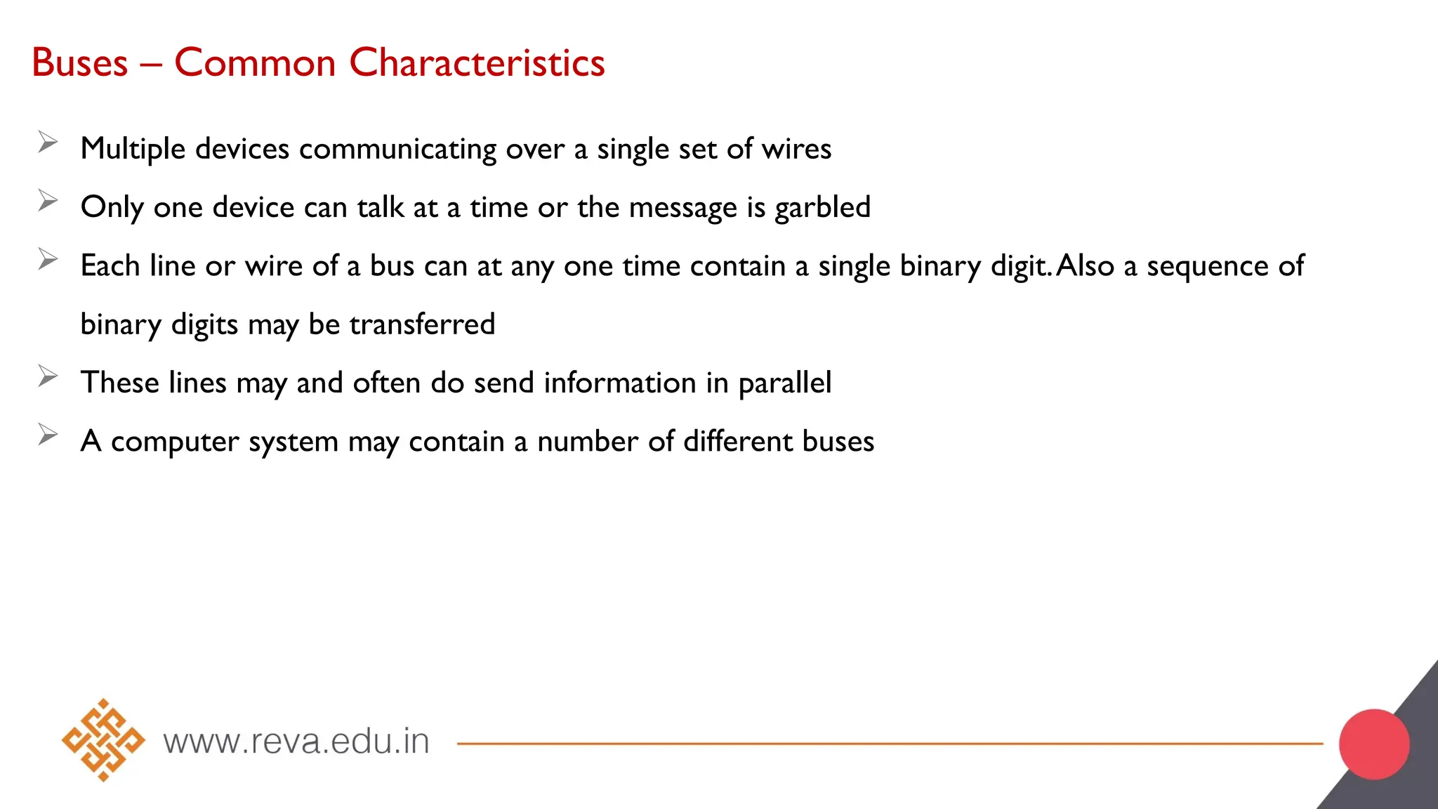
Buses – CommonCharacteristics
Multiple devices communicating over a single set of wires
Only one device can talk at a time or the message is garbled
Each line or wire of a bus can at any one time contain a single binary digit.Also a sequence of
binary digits may be transferred
These lines may and often do send information in parallel
A computer system may contain a number of different buses
8.
Buses – Structure
Serial versus parallel
Around 50-100 lines although it's
possible to have as few as 3 or 4
Lines can be classified into one of
four groups
Data lines
Address Lines
Control Lines
Power
Bus lines (parallel)
Data
Address
Control
Power
Bus lines (serial)
Data, address, and control are sequentially
sent down single wire
There may be additional control lines
Power
9.
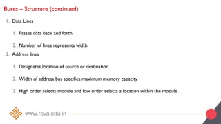
Buses – Structure(continued)
1. Data Lines
1. Passes data back and forth
2. Number of lines represents width
2. Address lines
1. Designates location of source or destination
2. Width of address bus specifies maximum memory capacity
3. High order selects module and low order selects a location within the module
10.
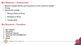
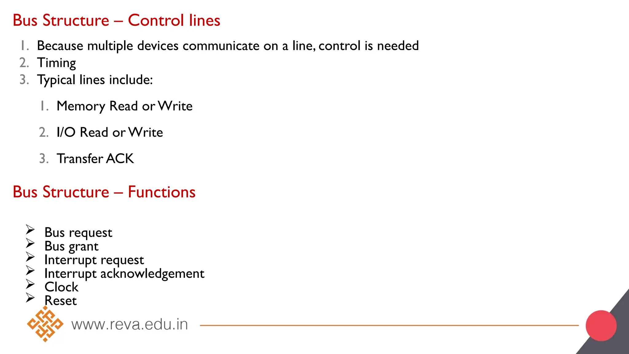
Bus Structure –Control lines
1. Because multiple devices communicate on a line, control is needed
2. Timing
3. Typical lines include:
1. Memory Read or Write
2. I/O Read or Write
3. Transfer ACK
Bus request
Bus grant
Interrupt request
Interrupt acknowledgement
Clock
Reset
Bus Structure – Functions
11.
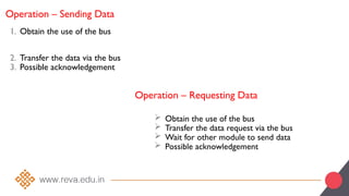
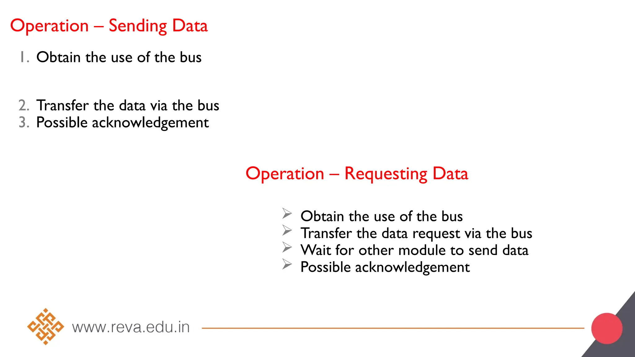
Operation – SendingData
1. Obtain the use of the bus
2. Transfer the data via the bus
3. Possible acknowledgement
Operation – Requesting Data
Obtain the use of the bus
Transfer the data request via the bus
Wait for other module to send data
Possible acknowledgement
12.
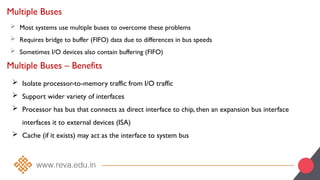
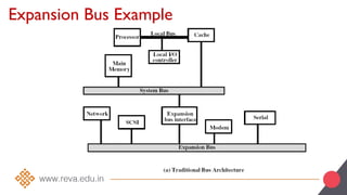
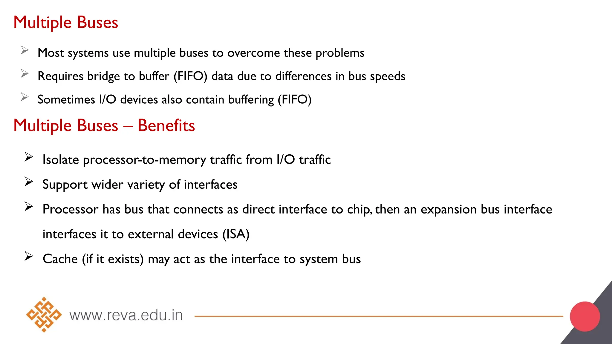
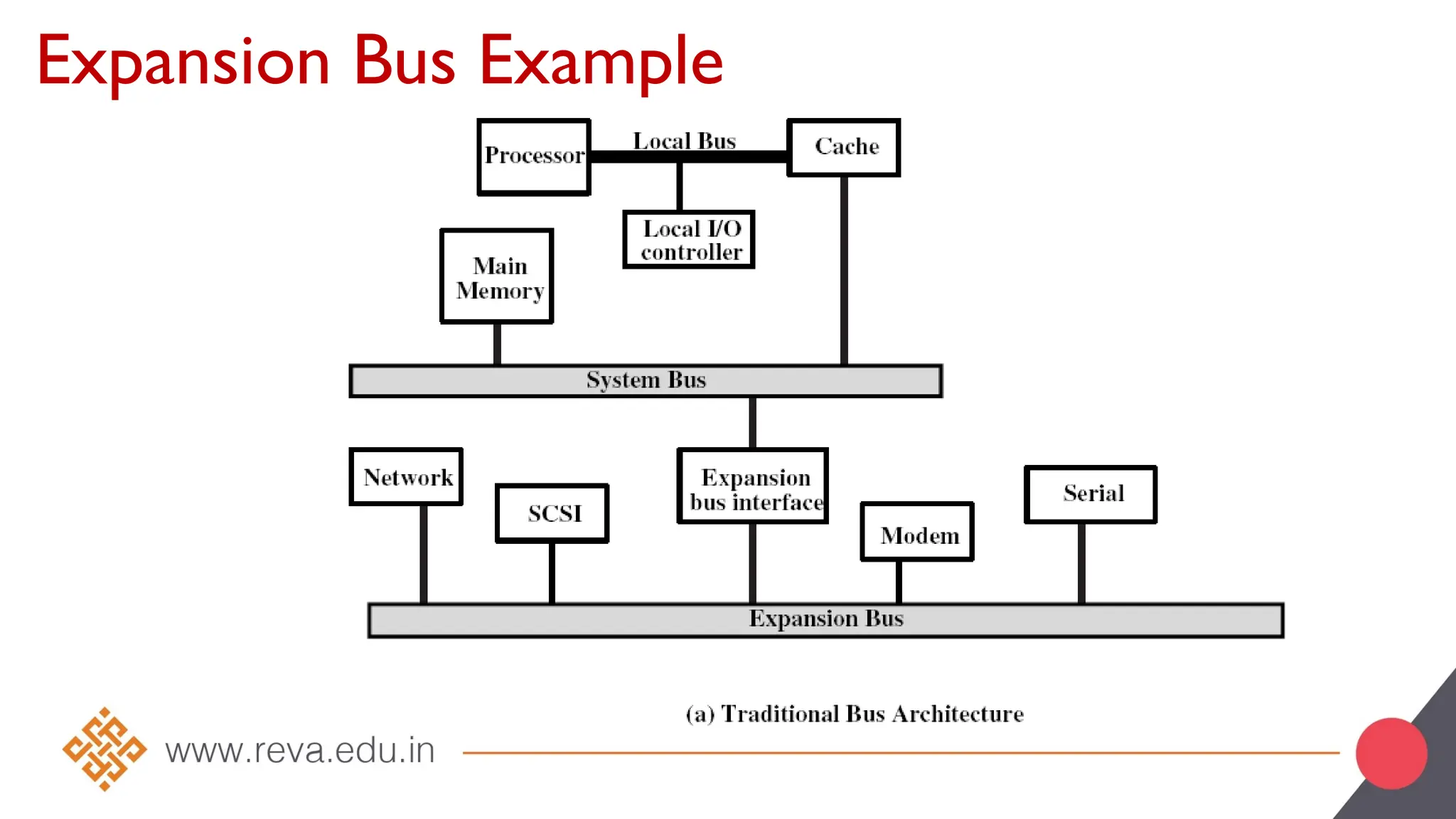
Multiple Buses
Mostsystems use multiple buses to overcome these problems
Requires bridge to buffer (FIFO) data due to differences in bus speeds
Sometimes I/O devices also contain buffering (FIFO)
Multiple Buses – Benefits
Isolate processor-to-memory traffic from I/O traffic
Support wider variety of interfaces
Processor has bus that connects as direct interface to chip, then an expansion bus interface
interfaces it to external devices (ISA)
Cache (if it exists) may act as the interface to system bus
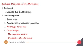
Bus Types- Dedicatedvs.Time Multiplexed
1. Dedicated
1. Separate data & address lines
2. Time multiplexed
1. Shared lines
2. Address valid or data valid control line
3. Advantage - fewer lines
4. Disadvantages
More complex control
Degradation of performance
15.
Bus Types-Physical Dedication
1.Physically separating buses and controlling them with a "channel changer”
2. Advantages – faster
3. Disadvantages – physically larger
Bus Arbitration
Listening to the bus is not usually a problem
Talking on the bus is a problem – need arbitration to allow more than one module
to control the bus at one time
Arbitration may be centralised or distributed
16.
Bus Timing
1. Co-ordinationof events on bus
2. Synchronous – controlled by a clock
3. Asynchronous – timing is handled by well-defined specifications, i.e., a response is
delivered within a specified time after a request
Synchronous Bus Timing
Events determined by clock signals
Control Bus includes clock line
A single 1-0 cycle is a bus cycle
All devices can read clock line
Usually sync on leading/rising edge
Usually a single cycle for an event
Analogy – Orchestra conductor with baton
Usually stricter in terms of its timing requirements
17.
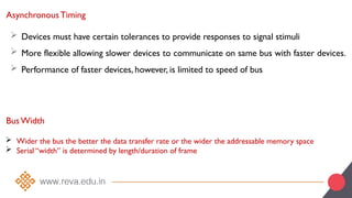
Asynchronous Timing
Devicesmust have certain tolerances to provide responses to signal stimuli
More flexible allowing slower devices to communicate on same bus with faster devices.
Performance of faster devices, however, is limited to speed of bus
Bus Width
Wider the bus the better the data transfer rate or the wider the addressable memory space
Serial “width” is determined by length/duration of frame
18.
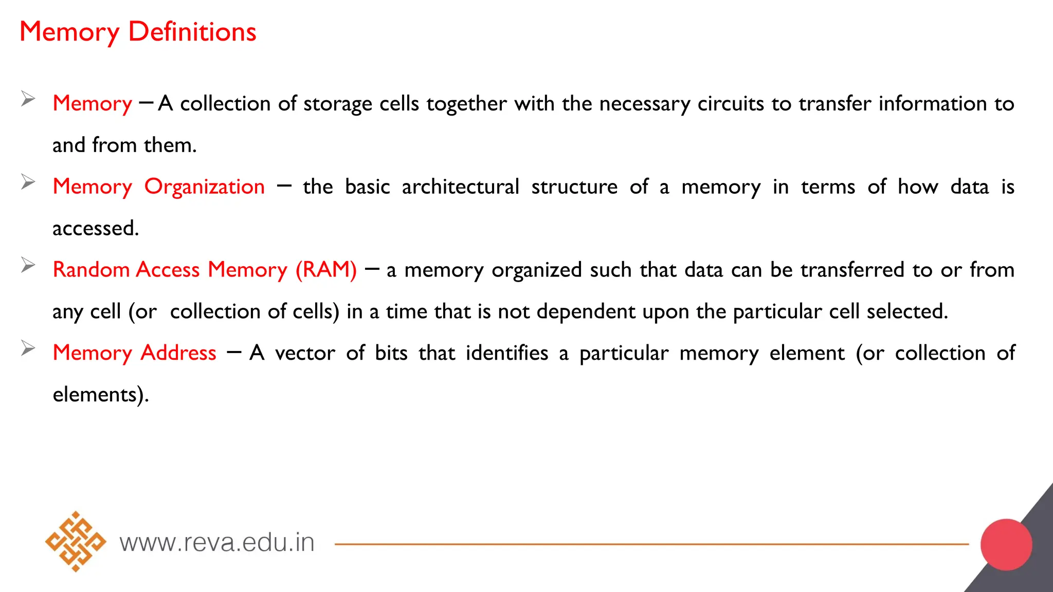
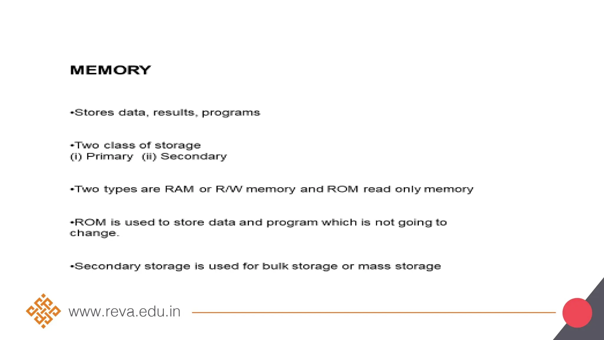
Memory Definitions
MemoryA collection of storage cells together with the necessary circuits to transfer information to
─
and from them.
Memory Organization the basic architectural structure of a memory in terms of how data is
─
accessed.
Random Access Memory (RAM) a memory organized such that data can be transferred to or from
─
any cell (or collection of cells) in a time that is not dependent upon the particular cell selected.
Memory Address A vector of bits that identifies a particular memory element (or collection of
─
elements).
19.
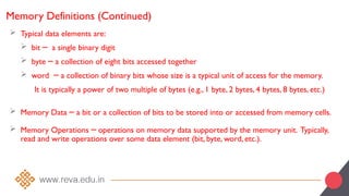
Memory Definitions (Continued)
Typical data elements are:
bit a single binary digit
─
byte a collection of eight bits accessed together
─
word a collection of binary bits whose size is a typical unit of access for the memory.
─
It is typically a power of two multiple of bytes (e.g., 1 byte, 2 bytes, 4 bytes, 8 bytes, etc.)
Memory Data a bit or a collection of bits to be stored into or accessed from memory cells.
─
Memory Operations operations on memory data supported by the memory unit. Typically,
─
read and write operations over some data element (bit, byte, word, etc.).
20.
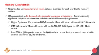
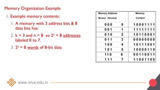
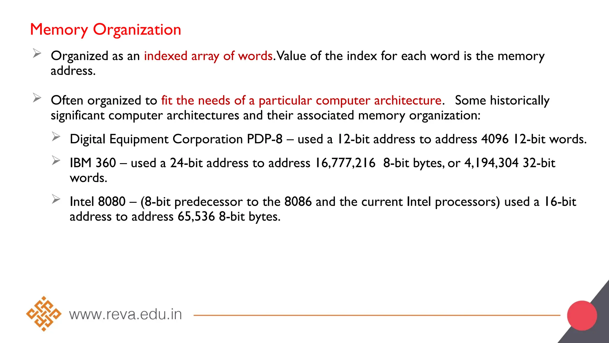
Memory Organization
Organizedas an indexed array of words.Value of the index for each word is the memory
address.
Often organized to fit the needs of a particular computer architecture. Some historically
significant computer architectures and their associated memory organization:
Digital Equipment Corporation PDP-8 – used a 12-bit address to address 4096 12-bit words.
IBM 360 – used a 24-bit address to address 16,777,216 8-bit bytes, or 4,194,304 32-bit
words.
Intel 8080 – (8-bit predecessor to the 8086 and the current Intel processors) used a 16-bit
address to address 65,536 8-bit bytes.
21.
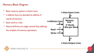
Memory Block Diagram
Basic memory system is shown here:
k address lines are decoded to address 2k
words of memory.
Each word is n bits.
Read and Write are single control lines defining
the simplest of memory operations.
n Data Input Lines
k Address Lines
Read
Write
n Data Output Lines
Memory
Unit
2k
Words
n Bits per Word
k
1
1
n
n
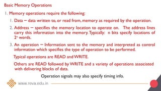
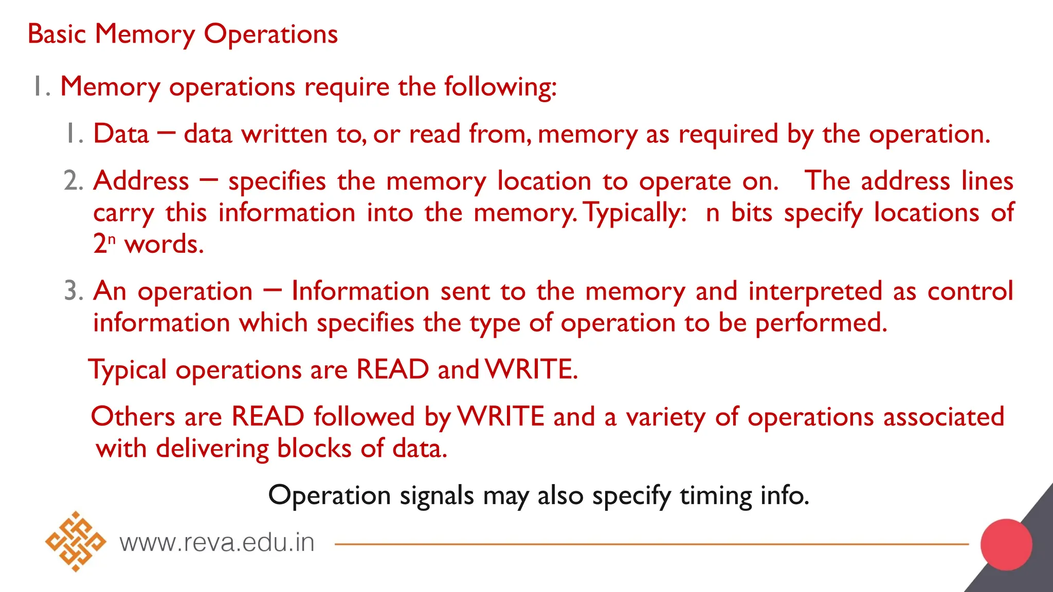
Basic Memory Operations
1.Memory operations require the following:
1. Data data written to, or read from, memory as required by the operation.
─
2. Address specifies the memory location to operate on. The address lines
─
carry this information into the memory.Typically: n bits specify locations of
2n
words.
3. An operation Information sent to the memory and interpreted as control
─
information which specifies the type of operation to be performed.
Typical operations are READ and WRITE.
Others are READ followed by WRITE and a variety of operations associated
with delivering blocks of data.
Operation signals may also specify timing info.
24.
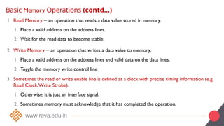
Basic Memory Operations(contd…)
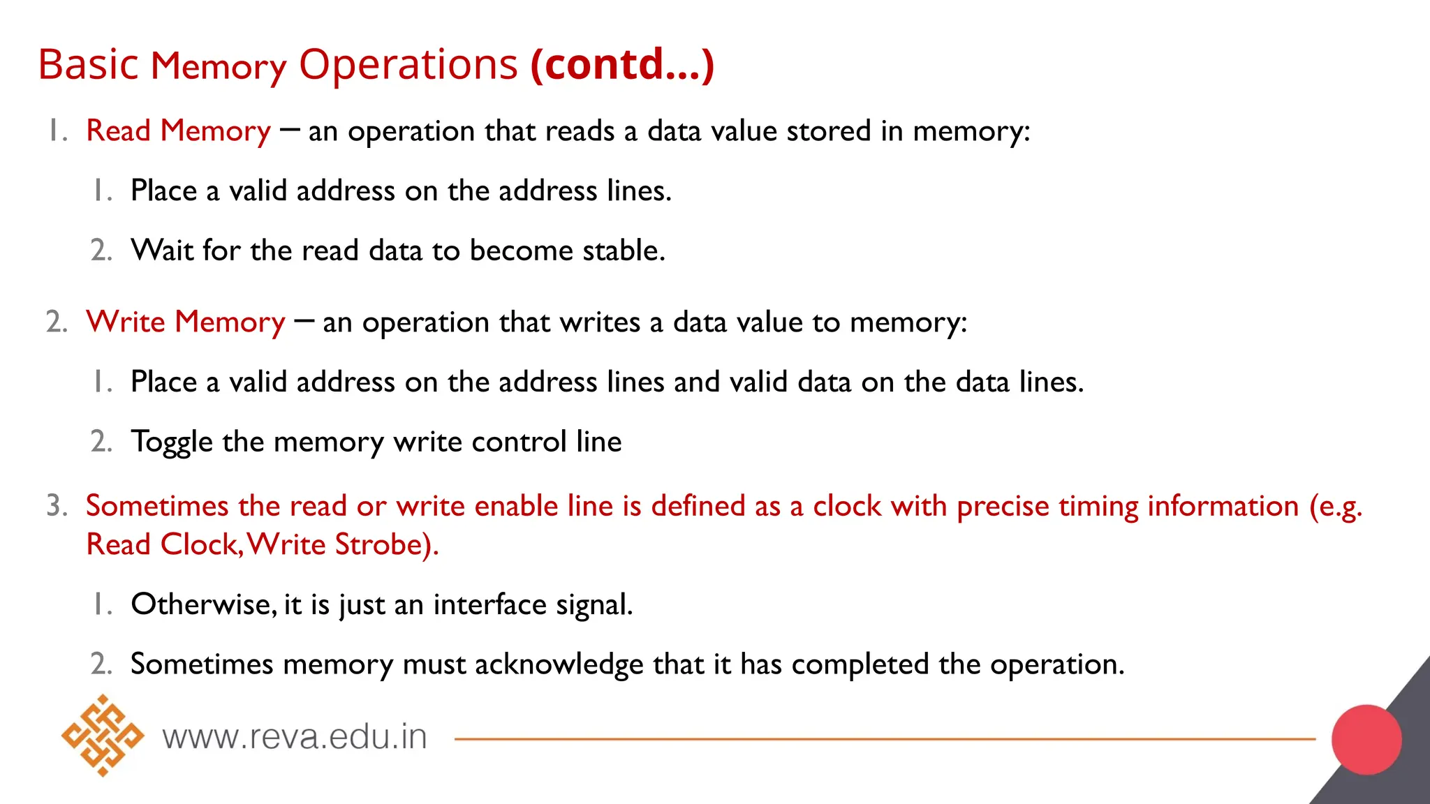
1. Read Memory an operation that reads a data value stored in memory:
─
1. Place a valid address on the address lines.
2. Wait for the read data to become stable.
2. Write Memory an operation that writes a data value to memory:
─
1. Place a valid address on the address lines and valid data on the data lines.
2. Toggle the memory write control line
3. Sometimes the read or write enable line is defined as a clock with precise timing information (e.g.
Read Clock,Write Strobe).
1. Otherwise, it is just an interface signal.
2. Sometimes memory must acknowledge that it has completed the operation.
25.
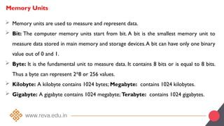
Memory Units
Memoryunits are used to measure and represent data.
Bit: The computer memory units start from bit. A bit is the smallest memory unit to
measure data stored in main memory and storage devices.A bit can have only one binary
value out of 0 and 1.
Byte: It is the fundamental unit to measure data. It contains 8 bits or is equal to 8 bits.
Thus a byte can represent 2*8 or 256 values.
Kilobyte: A kilobyte contains 1024 bytes; Megabyte: contains 1024 kilobytes.
Gigabyte: A gigabyte contains 1024 megabyte; Terabyte: contains 1024 gigabytes.
26.
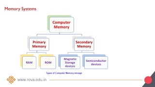
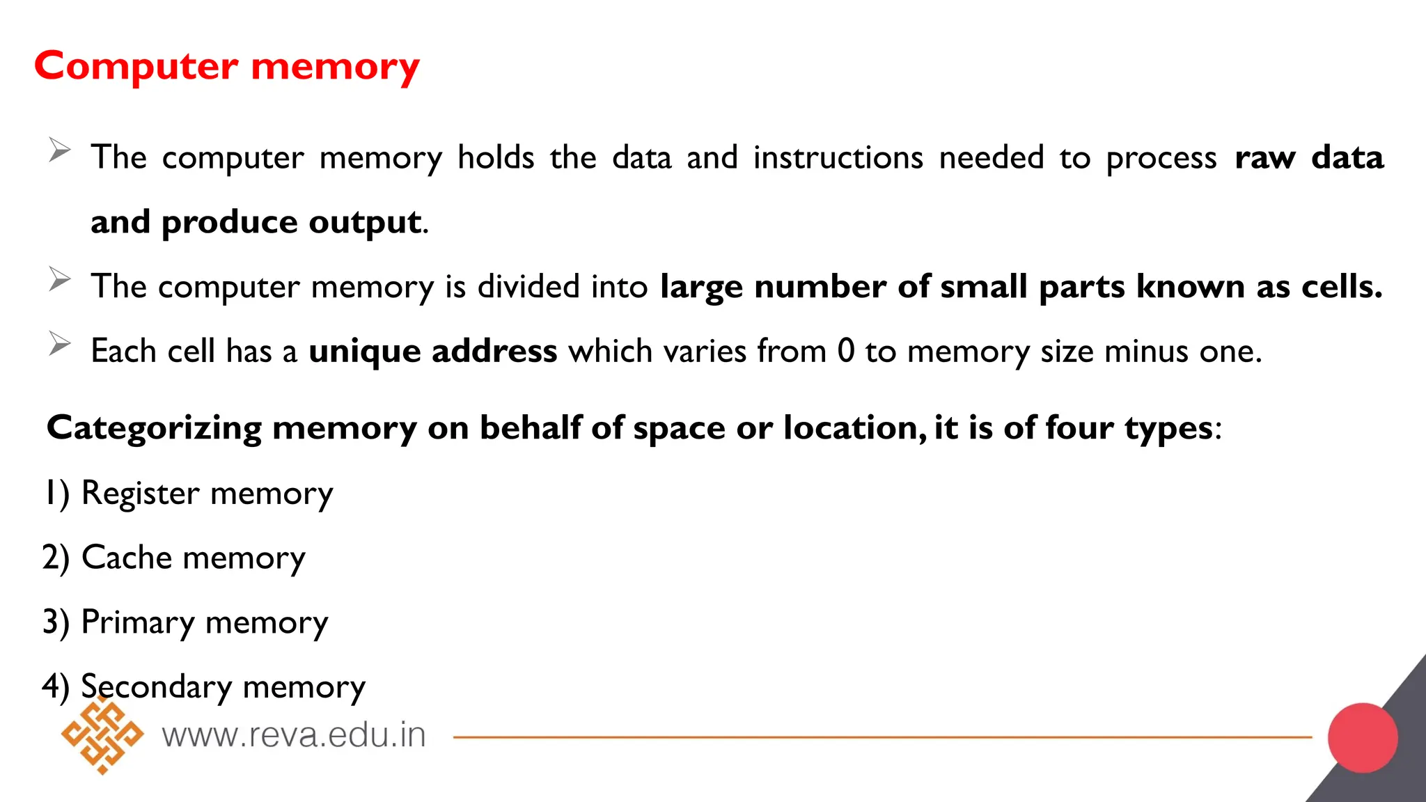
Computer memory
Thecomputer memory holds the data and instructions needed to process raw data
and produce output.
The computer memory is divided into large number of small parts known as cells.
Each cell has a unique address which varies from 0 to memory size minus one.
Categorizing memory on behalf of space or location, it is of four types:
1) Register memory
2) Cache memory
3) Primary memory
4) Secondary memory
27.
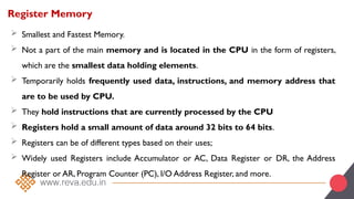
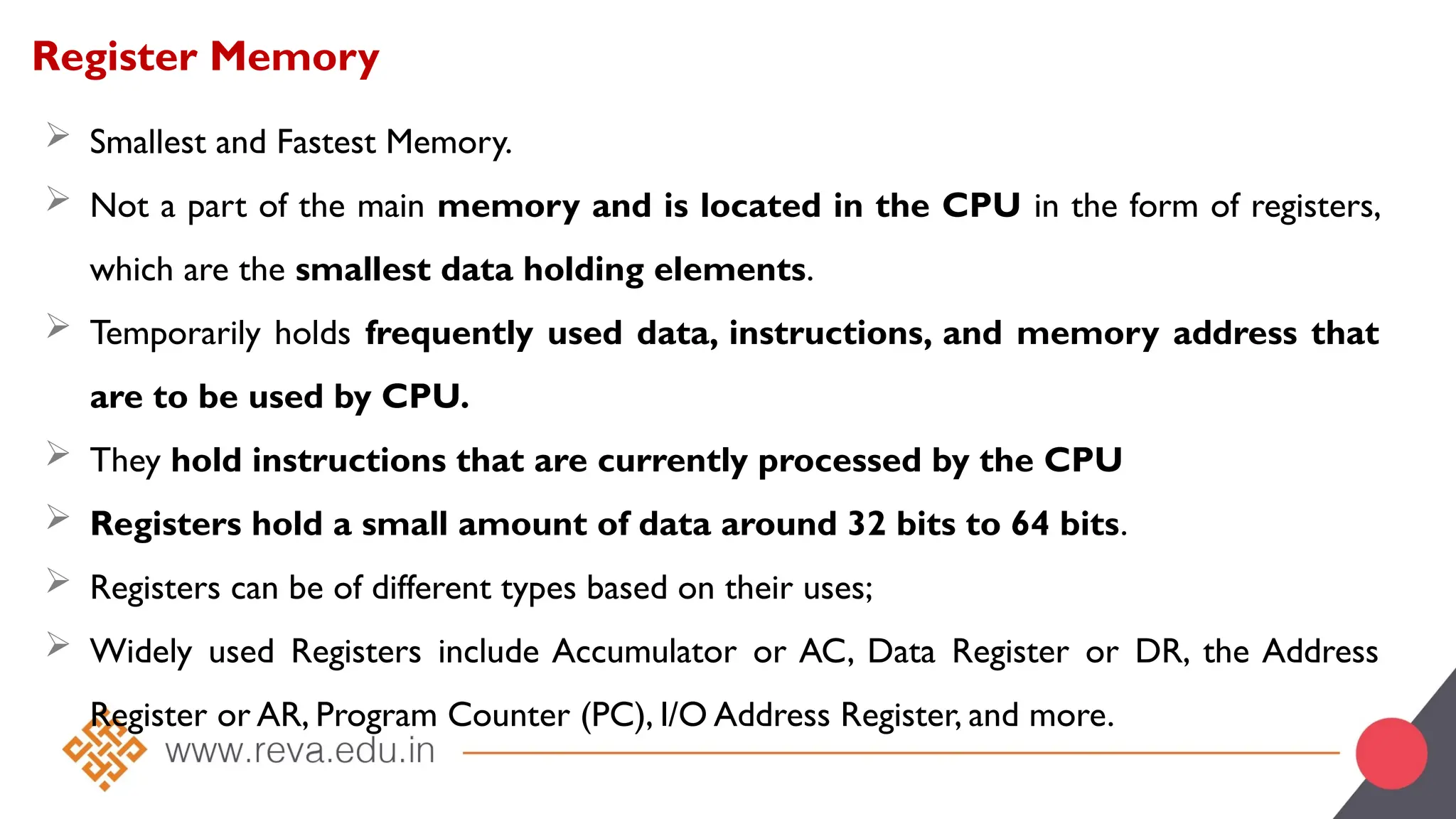
Register Memory
Smallestand Fastest Memory.
Not a part of the main memory and is located in the CPU in the form of registers,
which are the smallest data holding elements.
Temporarily holds frequently used data, instructions, and memory address that
are to be used by CPU.
They hold instructions that are currently processed by the CPU
Registers hold a small amount of data around 32 bits to 64 bits.
Registers can be of different types based on their uses;
Widely used Registers include Accumulator or AC, Data Register or DR, the Address
Register or AR, Program Counter (PC), I/O Address Register, and more.
28.
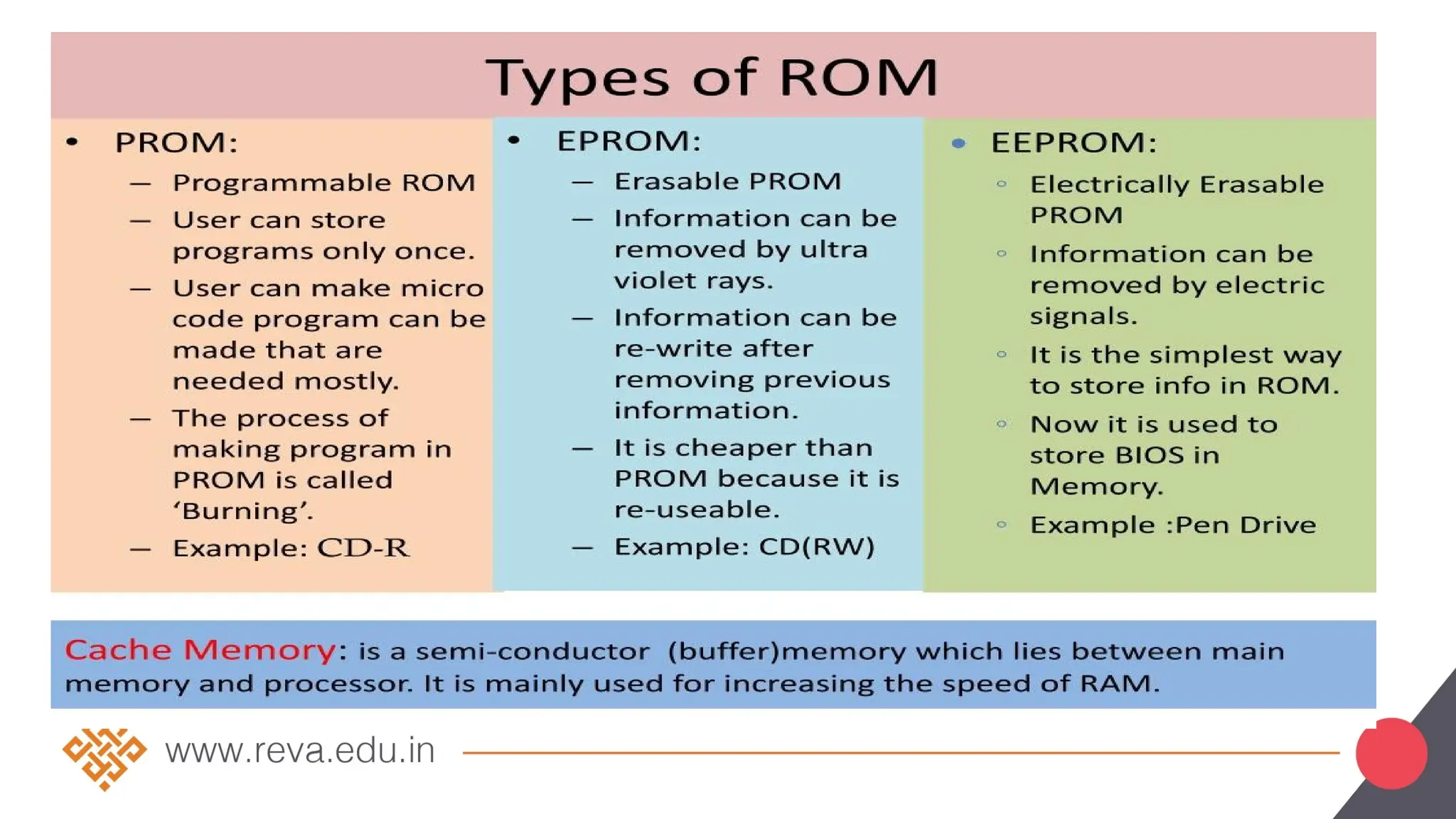
Cache Memory
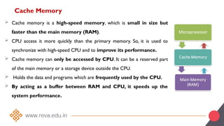
Cachememory is a high-speed memory, which is small in size but
faster than the main memory (RAM).
CPU access it more quickly than the primary memory. So, it is used to
synchronize with high-speed CPU and to improve its performance.
Cache memory can only be accessed by CPU. It can be a reserved part
of the main memory or a storage device outside the CPU.
Holds the data and programs which are frequently used by the CPU.
By acting as a buffer between RAM and CPU, it speeds up the
system performance.
29.
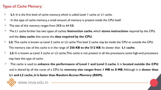
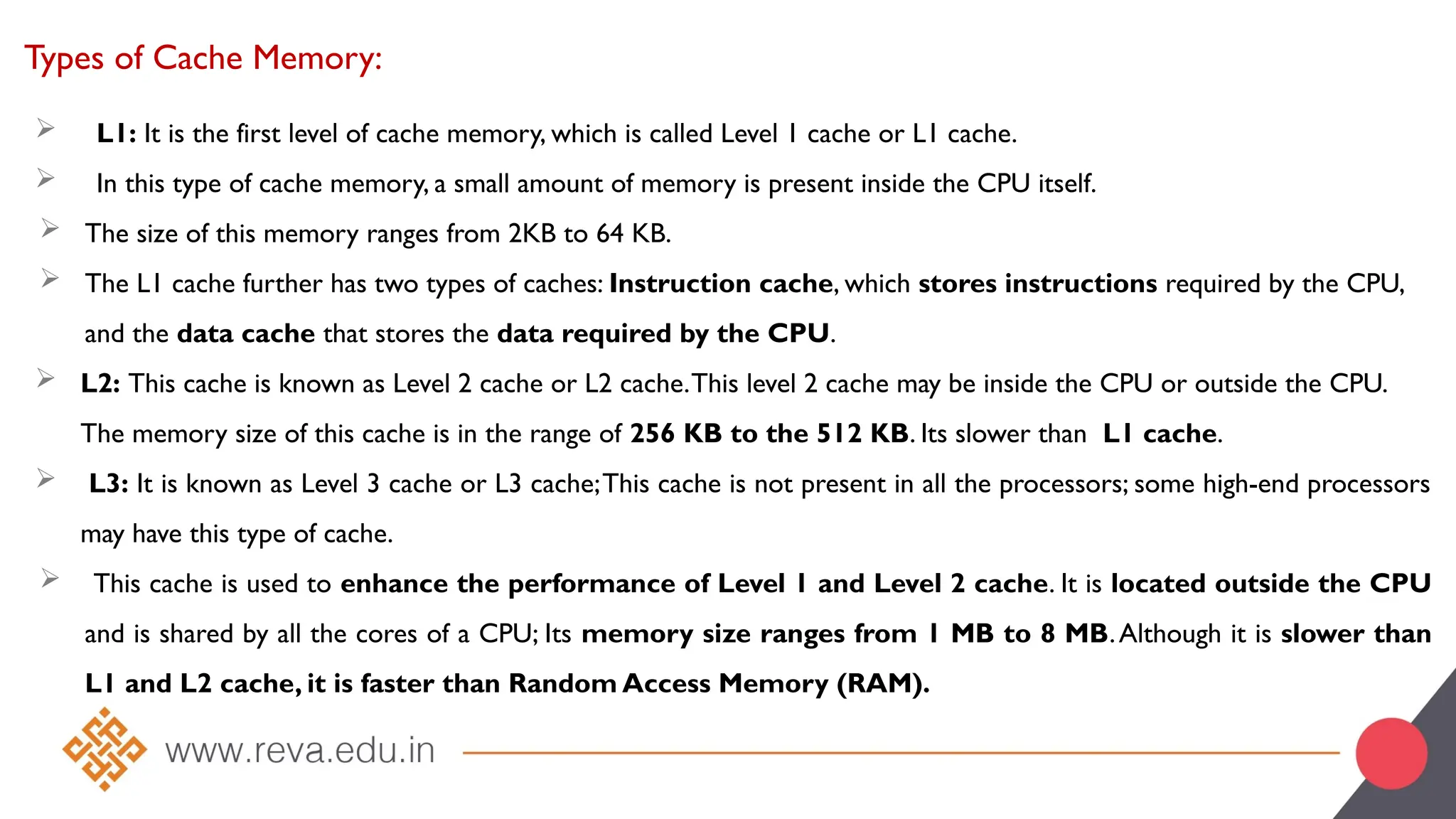
Types of CacheMemory:
L1: It is the first level of cache memory, which is called Level 1 cache or L1 cache.
In this type of cache memory, a small amount of memory is present inside the CPU itself.
The size of this memory ranges from 2KB to 64 KB.
The L1 cache further has two types of caches: Instruction cache, which stores instructions required by the CPU,
and the data cache that stores the data required by the CPU.
L2: This cache is known as Level 2 cache or L2 cache.This level 2 cache may be inside the CPU or outside the CPU.
The memory size of this cache is in the range of 256 KB to the 512 KB. Its slower than L1 cache.
L3: It is known as Level 3 cache or L3 cache;This cache is not present in all the processors; some high-end processors
may have this type of cache.
This cache is used to enhance the performance of Level 1 and Level 2 cache. It is located outside the CPU
and is shared by all the cores of a CPU; Its memory size ranges from 1 MB to 8 MB.Although it is slower than
L1 and L2 cache, it is faster than Random Access Memory (RAM).
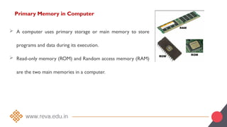
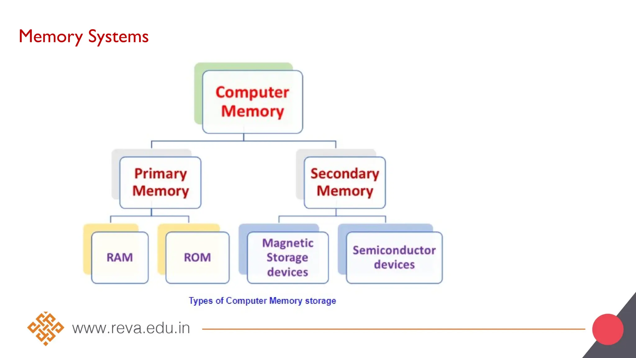
Primary Memory inComputer
A computer uses primary storage or main memory to store
programs and data during its execution.
Read-only memory (ROM) and Random access memory (RAM)
are the two main memories in a computer.
32.
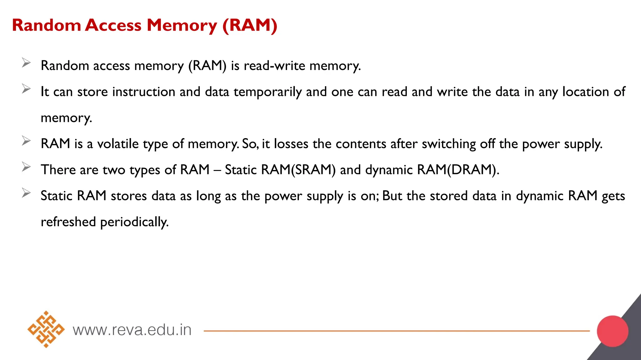
Random Access Memory(RAM)
Random access memory (RAM) is read-write memory.
It can store instruction and data temporarily and one can read and write the data in any location of
memory.
RAM is a volatile type of memory. So, it losses the contents after switching off the power supply.
There are two types of RAM – Static RAM(SRAM) and dynamic RAM(DRAM).
Static RAM stores data as long as the power supply is on; But the stored data in dynamic RAM gets
refreshed periodically.
33.
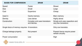
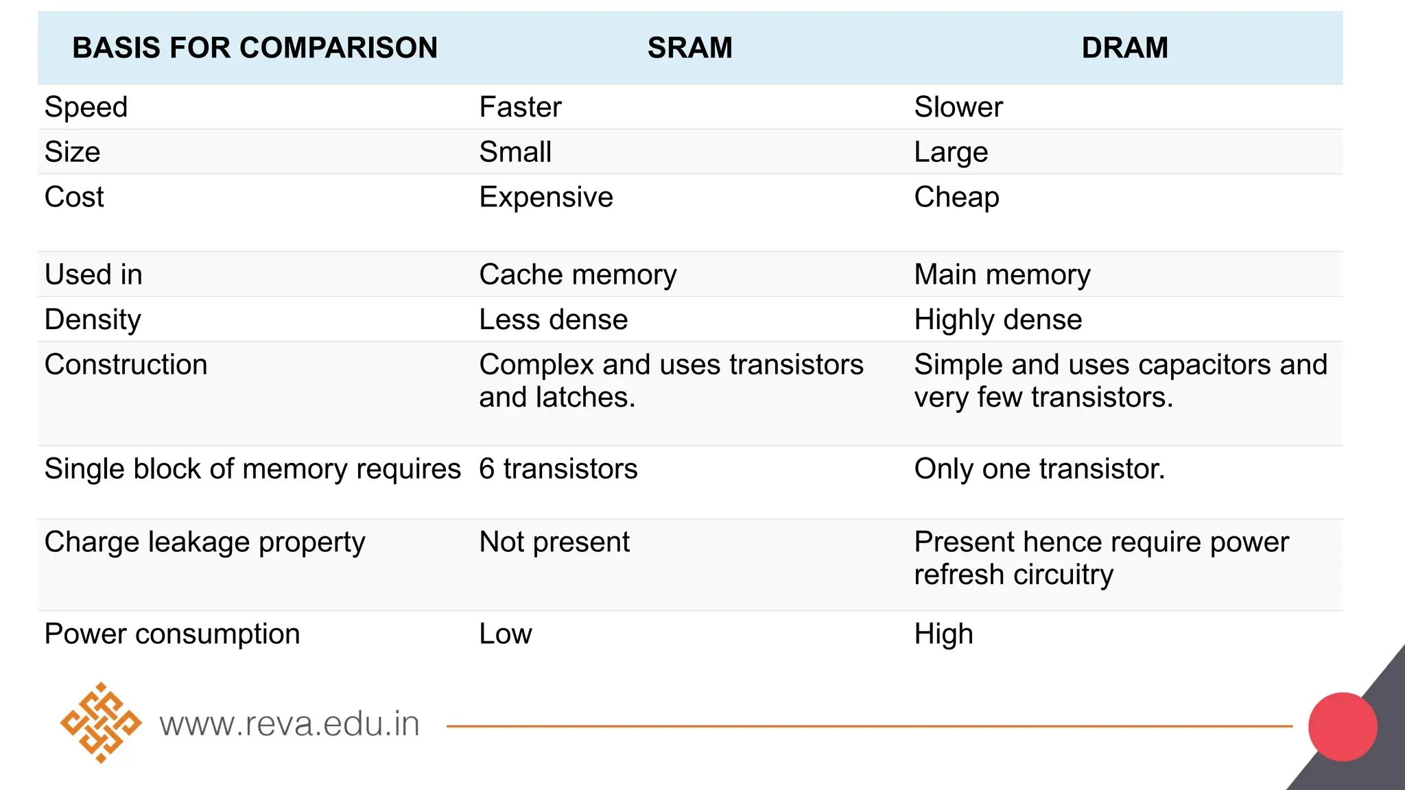
BASIS FOR COMPARISONSRAM DRAM
Speed Faster Slower
Size Small Large
Cost Expensive Cheap
Used in Cache memory Main memory
Density Less dense Highly dense
Construction Complex and uses transistors
and latches.
Simple and uses capacitors and
very few transistors.
Single block of memory requires 6 transistors Only one transistor.
Charge leakage property Not present Present hence require power
refresh circuitry
Power consumption Low High
34.
SDRAM
The SynchronousDynamic Random Access Memory, commonly abbreviated as SDRAM,
is a type of dynamic random access memory (DRAM).
SDRAM is the form of RAM frequently seen in most computers that provides faster
speed when compared to regular DRAM.
SDRAMs offer greater data transfer rates and concurrency.
SDRAM provides a simple design at a low cost, which can greatly benefit manufacturers.
Advantages have made SDRAM a popular and preferred choice in the computer memory
market, particularly for RAM.
35.
ROM(Read Only Memory)
ROM, which stands for read only memory, is a memory device or
storage medium that stores information permanently.
Only read the programs and data stored on it but cannot write on
it. It is restricted to reading words that are permanently stored within
the unit.
The manufacturer of ROM fills the programs into the ROM at
the time of manufacturing the ROM.
After this, the content of the ROM can't be altered, which means you
can't reprogram, rewrite, or erase its content later. However, there
are some types of ROM where you can modify the data.
36.
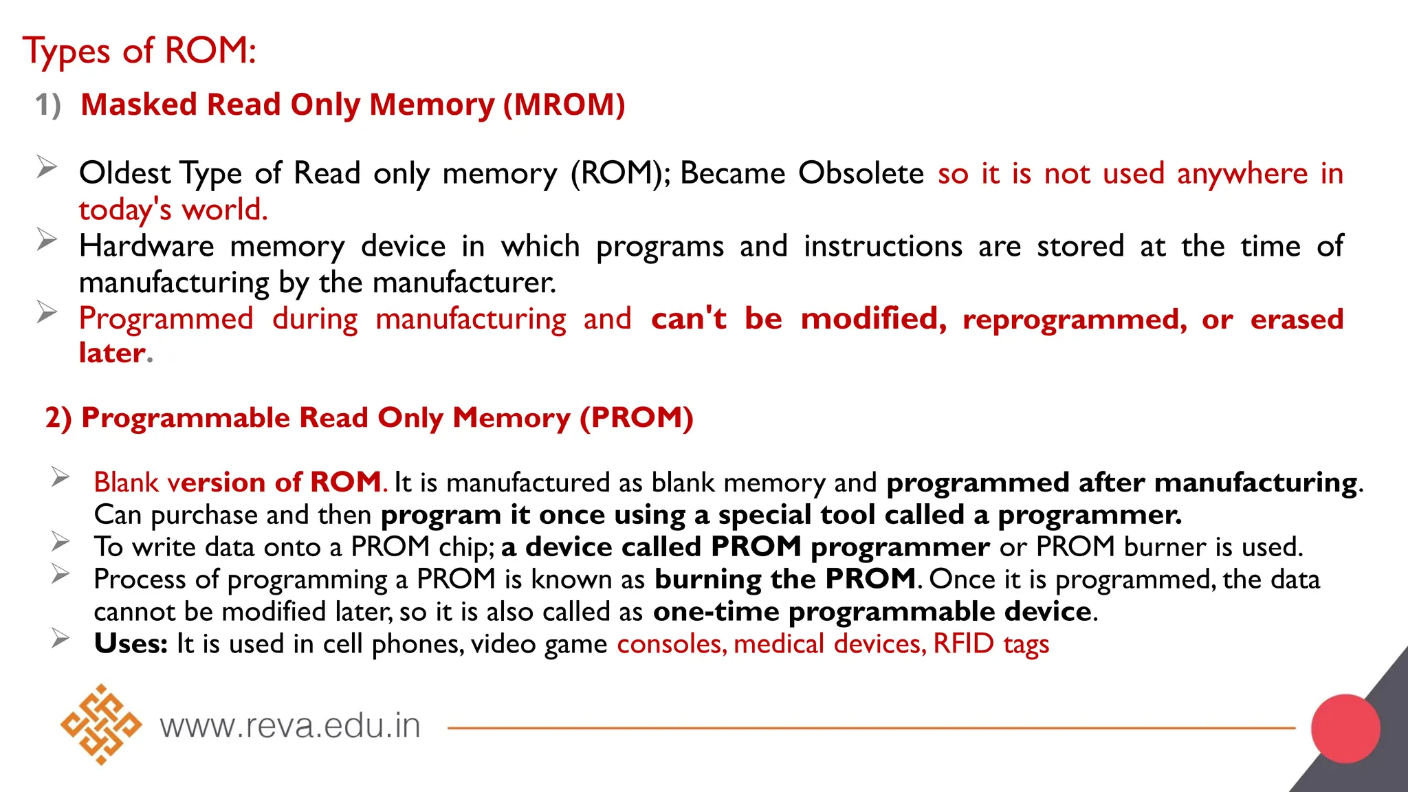
Types of ROM:
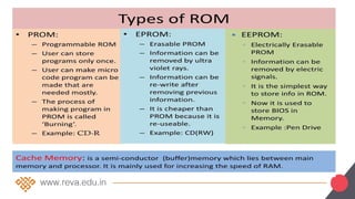
1)Masked Read Only Memory (MROM)
Oldest Type of Read only memory (ROM); Became Obsolete so it is not used anywhere in
today's world.
Hardware memory device in which programs and instructions are stored at the time of
manufacturing by the manufacturer.
Programmed during manufacturing and can't be modified, reprogrammed, or erased
later.
2) Programmable Read Only Memory (PROM)
Blank version of ROM. It is manufactured as blank memory and programmed after manufacturing.
Can purchase and then program it once using a special tool called a programmer.
To write data onto a PROM chip; a device called PROM programmer or PROM burner is used.
Process of programming a PROM is known as burning the PROM. Once it is programmed, the data
cannot be modified later, so it is also called as one-time programmable device.
Uses: It is used in cell phones, video game consoles, medical devices, RFID tags
37.
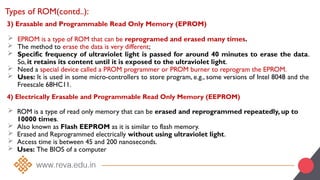
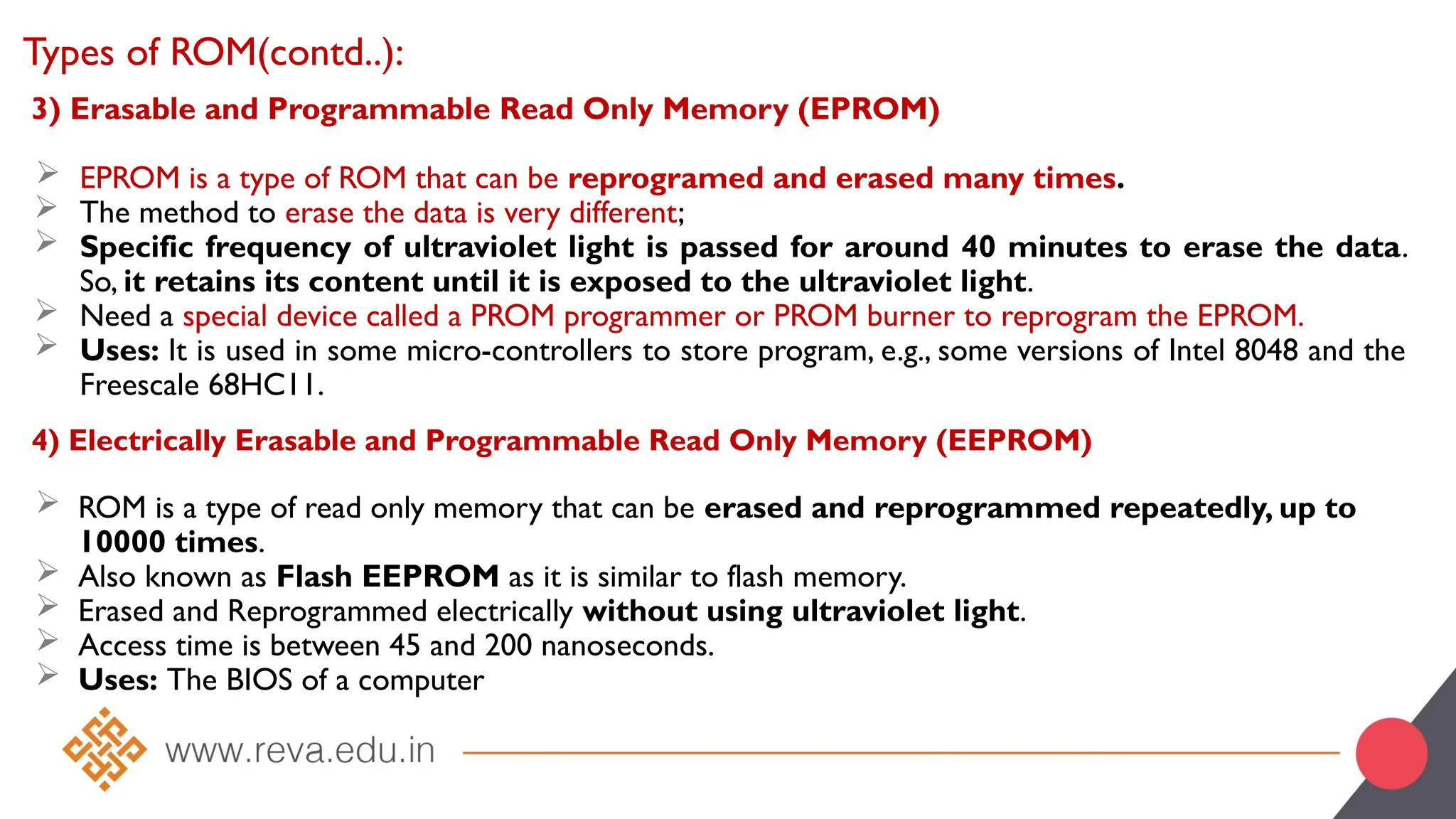
3) Erasable andProgrammable Read Only Memory (EPROM)
EPROM is a type of ROM that can be reprogramed and erased many times.
The method to erase the data is very different;
Specific frequency of ultraviolet light is passed for around 40 minutes to erase the data.
So, it retains its content until it is exposed to the ultraviolet light.
Need a special device called a PROM programmer or PROM burner to reprogram the EPROM.
Uses: It is used in some micro-controllers to store program, e.g., some versions of Intel 8048 and the
Freescale 68HC11.
Types of ROM(contd..):
4) Electrically Erasable and Programmable Read Only Memory (EEPROM)
ROM is a type of read only memory that can be erased and reprogrammed repeatedly, up to
10000 times.
Also known as Flash EEPROM as it is similar to flash memory.
Erased and Reprogrammed electrically without using ultraviolet light.
Access time is between 45 and 200 nanoseconds.
Uses: The BIOS of a computer
38.
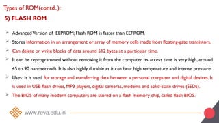
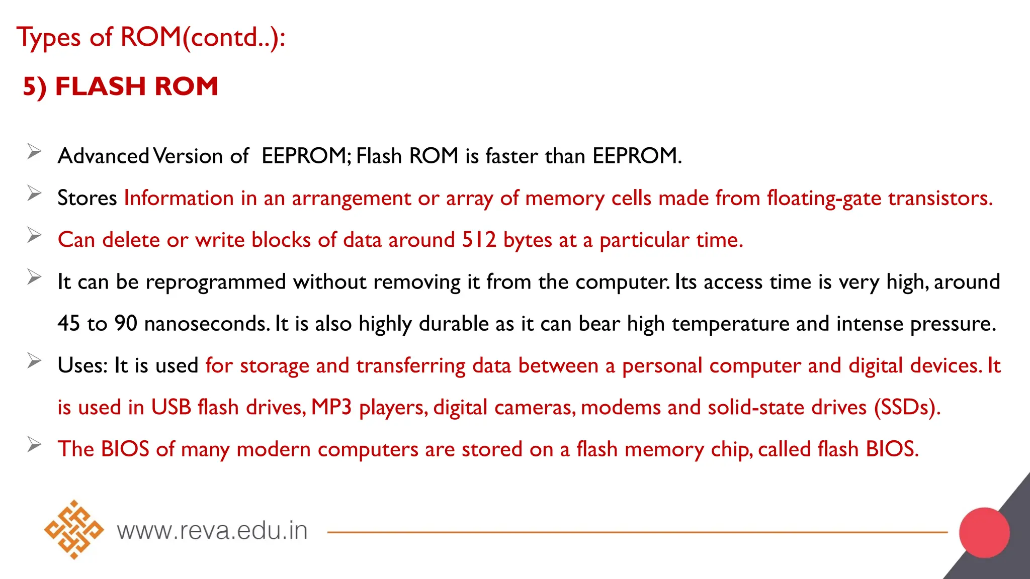
5) FLASH ROM
AdvancedVersion of EEPROM; Flash ROM is faster than EEPROM.
Stores Information in an arrangement or array of memory cells made from floating-gate transistors.
Can delete or write blocks of data around 512 bytes at a particular time.
It can be reprogrammed without removing it from the computer. Its access time is very high, around
45 to 90 nanoseconds. It is also highly durable as it can bear high temperature and intense pressure.
Uses: It is used for storage and transferring data between a personal computer and digital devices. It
is used in USB flash drives, MP3 players, digital cameras, modems and solid-state drives (SSDs).
The BIOS of many modern computers are stored on a flash memory chip, called flash BIOS.
Types of ROM(contd..):
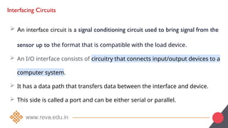
Interfacing Circuits
Aninterface circuit is a signal conditioning circuit used to bring signal from the
sensor up to the format that is compatible with the load device.
An I/O interface consists of circuitry that connects input/output devices to a
computer system.
It has a data path that transfers data between the interface and device.
This side is called a port and can be either serial or parallel.
57.
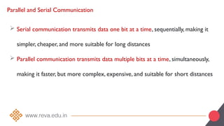
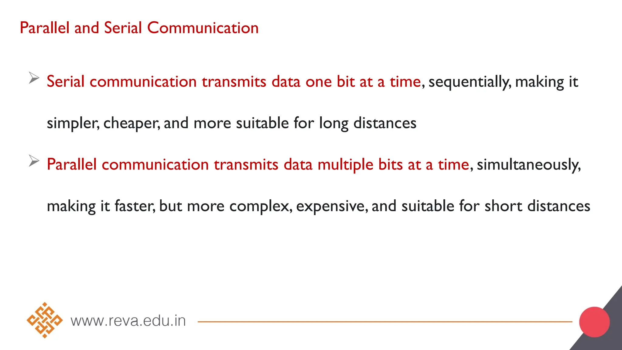
Parallel and SerialCommunication
Serial communication transmits data one bit at a time, sequentially, making it
simpler, cheaper, and more suitable for long distances
Parallel communication transmits data multiple bits at a time, simultaneously,
making it faster, but more complex, expensive, and suitable for short distances
58.
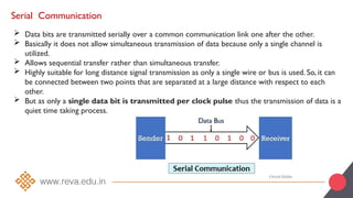
Serial Communication
Databits are transmitted serially over a common communication link one after the other.
Basically it does not allow simultaneous transmission of data because only a single channel is
utilized.
Allows sequential transfer rather than simultaneous transfer.
Highly suitable for long distance signal transmission as only a single wire or bus is used. So, it can
be connected between two points that are separated at a large distance with respect to each
other.
But as only a single data bit is transmitted per clock pulse thus the transmission of data is a
quiet time taking process.
59.
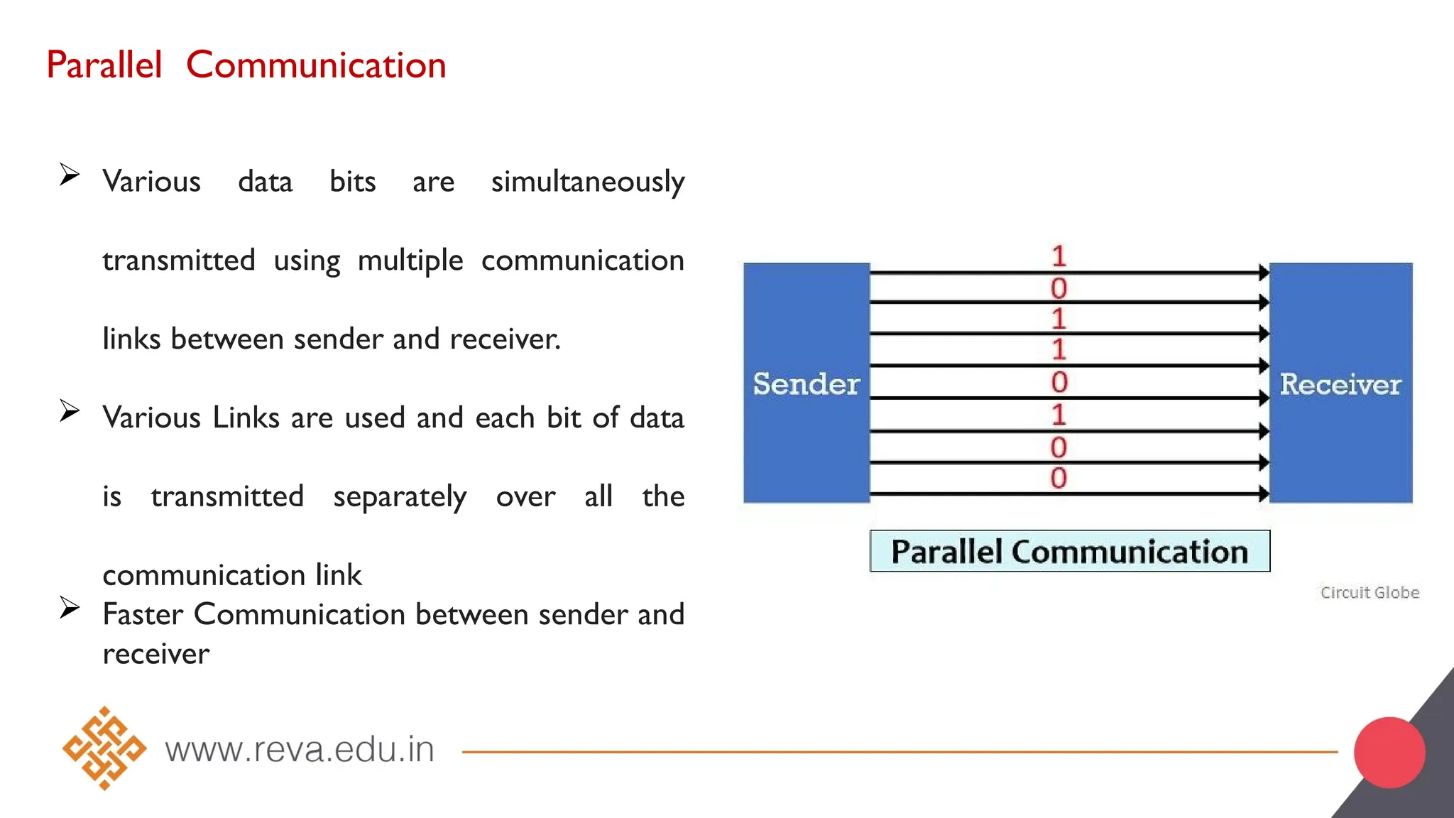
Parallel Communication
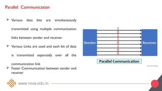
Variousdata bits are simultaneously
transmitted using multiple communication
links between sender and receiver.
Various Links are used and each bit of data
is transmitted separately over all the
communication link
Faster Communication between sender and
receiver
60.
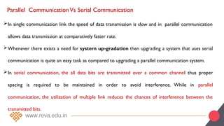
Parallel CommunicationVs SerialCommunication
In single communication link the speed of data transmission is slow and in parallel communication
allows data transmission at comparatively faster rate.
Whenever there exists a need for system up-gradation then upgrading a system that uses serial
communication is quite an easy task as compared to upgrading a parallel communication system.
In serial communication, the all data bits are transmitted over a common channel thus proper
spacing is required to be maintained in order to avoid interference. While in parallel
communication, the utilization of multiple link reduces the chances of interference between the
transmitted bits.
61.
Parallel CommunicationVs SerialCommunication(contd…)
Serial communication supports higher bandwidth while parallel communication supports
comparatively lower bandwidth.
Serial communication is efficient for high frequency operation. However, parallel communication
shows its suitability more in case of low frequency operations.
Due to existence of single link, the problem of crosstalk is not present in serial communication.
But multiple links increase the chances of crosstalk in parallel communication.
Serial communication is suitable for long distance transmission of data as against parallel
communication is suitable for short distance transmission of data.
62.
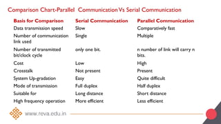
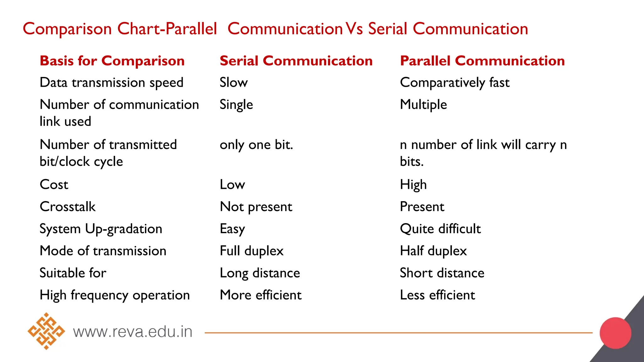
Comparison Chart-Parallel CommunicationVsSerial Communication
Basis for Comparison Serial Communication Parallel Communication
Data transmission speed Slow Comparatively fast
Number of communication
link used
Single Multiple
Number of transmitted
bit/clock cycle
only one bit. n number of link will carry n
bits.
Cost Low High
Crosstalk Not present Present
System Up-gradation Easy Quite difficult
Mode of transmission Full duplex Half duplex
Suitable for Long distance Short distance
High frequency operation More efficient Less efficient
66.
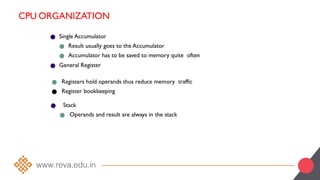
CPU ORGANIZATION
● SingleAccumulator
● Result usually goes to the Accumulator
● Accumulator has to be saved to memory quite often
● General Register
● Registers hold operands thus reduce memory traffic
● Register bookkeeping
● Stack
● Operands and result are always in the stack
67.
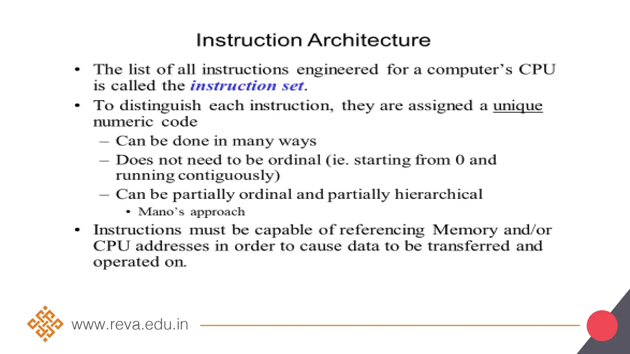
INSTRUCTION FORMATS
● Three-AddressInstructions
● ADD R1, R2, R3 R1 R2 + R3
←
● Two-Address Instructions
● ADD R1, R2 R1 R1 + R2
←
● One-Address Instructions
● ADD M AC AC + M[AR]
←
Zero-Address Instructions
● ADD TOS TOS + (TOS – 1)
←
RISC Instructions
● Lots of registers. Memory is restricted to Load & Store
●
Opcode Operand(s) or Address(es)
68.
INSTRUCTION FORMATS
Example: Evaluate(A+B) * (C+D)
● Three-Address
l ADD R1, A, B
ADD R2, C, D
MUL X, R1, R2
; R1 ← M[A] + M[B]
; R2 ← M[C] + M[D]
; M[X] ← R1 * R2
l
l
69.
INSTRUCTION FORMATS
Example: Evaluate(A+B) * (C+D)
●
Two-Address
l
MOVR1, A
ADD R1, B
MOVR2, C
ADD R2, D
MUL R1, R2
MOVX, R1
; R1 ← M[A]
; R1 ← R1 + M[B]
; R2 ← M[C]
; R2 ← R2 + M[D]
; R1 ← R1 * R2
; M[X] ← R1
l
l
l
l
l
70.
INSTRUCTION FORMATS
Example: Evaluate(A+B) * (C+D)
● One-Address
l LOAD A
ADD B
; AC ← M[A]
; AC ← AC + M[B]
; M[T] ← AC
; AC ← M[C]
; AC ← AC + M[D]
; AC ← AC * M[T]
; M[X] ← AC
l
l STORET
l LOAD C
ADD D
MUL T
l
l
l STOREX
71.
INSTRUCTION FORMATS
Example: Evaluate(A+B) * (C+D)
●
Zero-Address
l
PUSH A
PUSH B
ADD PUSH
C
PUSH D
ADD
;TOS A
←
;TOS B
←
;TOS (A + B)
←
;TOS C
←
;TOS D
←
;TOS (C + D)
←
;TOS ←
l
l
l
l
l
l
MUL (C+D)*(A+B)
POP X
l
; M[X] TOS
←
72.
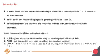
Instruction Sets
Aset of codes that can only be understood by a processor of the computer or CPU is known as
an instruction set.
These codes and machine languages are generally present as 1s and 0s.
The movements of bits and bytes are controlled by these instruction sets present in the
processor.
Some common examples of instruction sets are:
1. JUMP – jump instruction set is used to jump to any designated address of RAM.
2. ADD – add instruction set is used to add any two numbers together.
3. LOAD – load instruction set is used to load any required information from the RAM to the
CPU.
73.
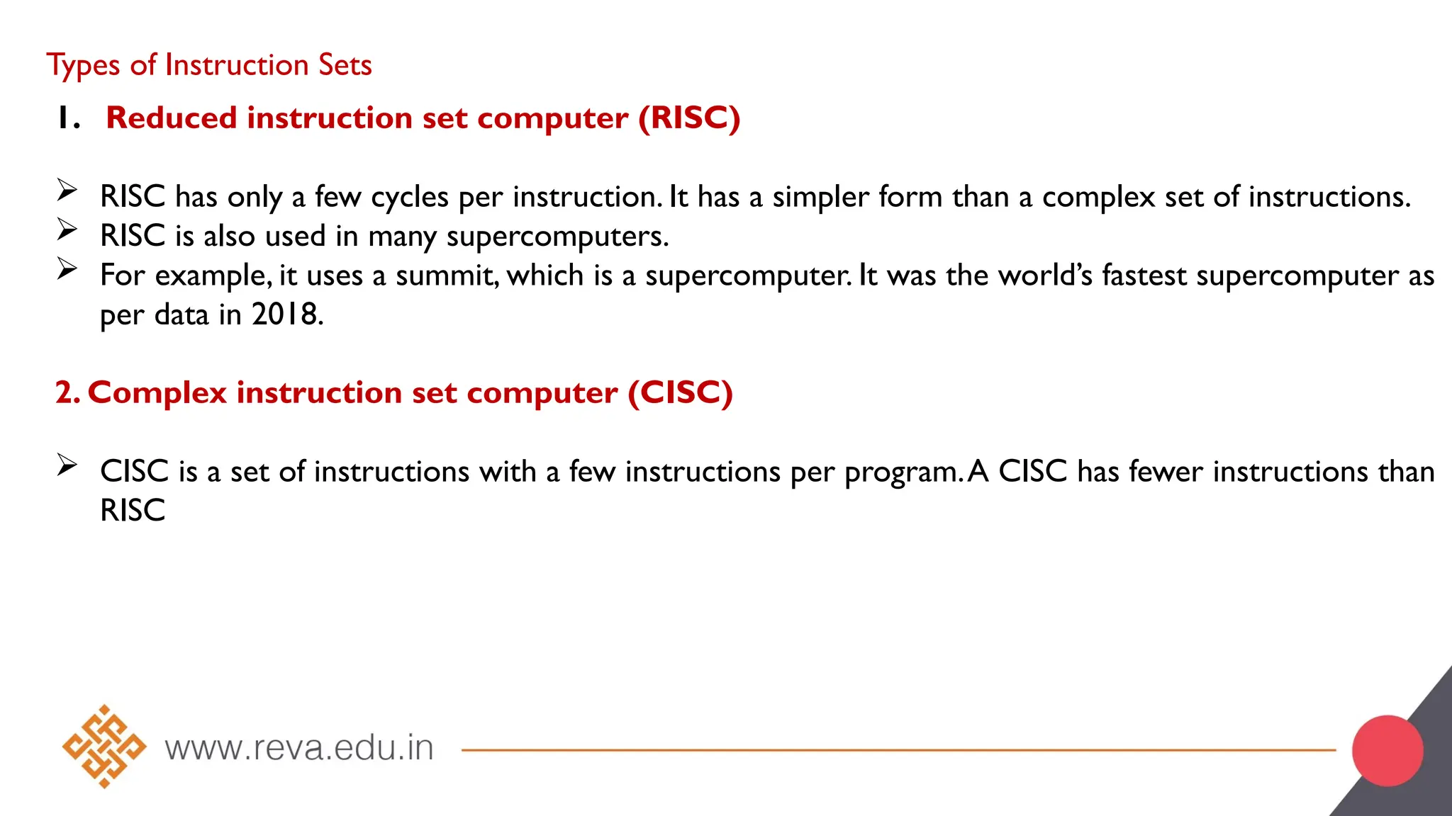
Types of InstructionSets
1. Reduced instruction set computer (RISC)
RISC has only a few cycles per instruction. It has a simpler form than a complex set of instructions.
RISC is also used in many supercomputers.
For example, it uses a summit, which is a supercomputer. It was the world’s fastest supercomputer as
per data in 2018.
2. Complex instruction set computer (CISC)
CISC is a set of instructions with a few instructions per program.A CISC has fewer instructions than
RISC
74.
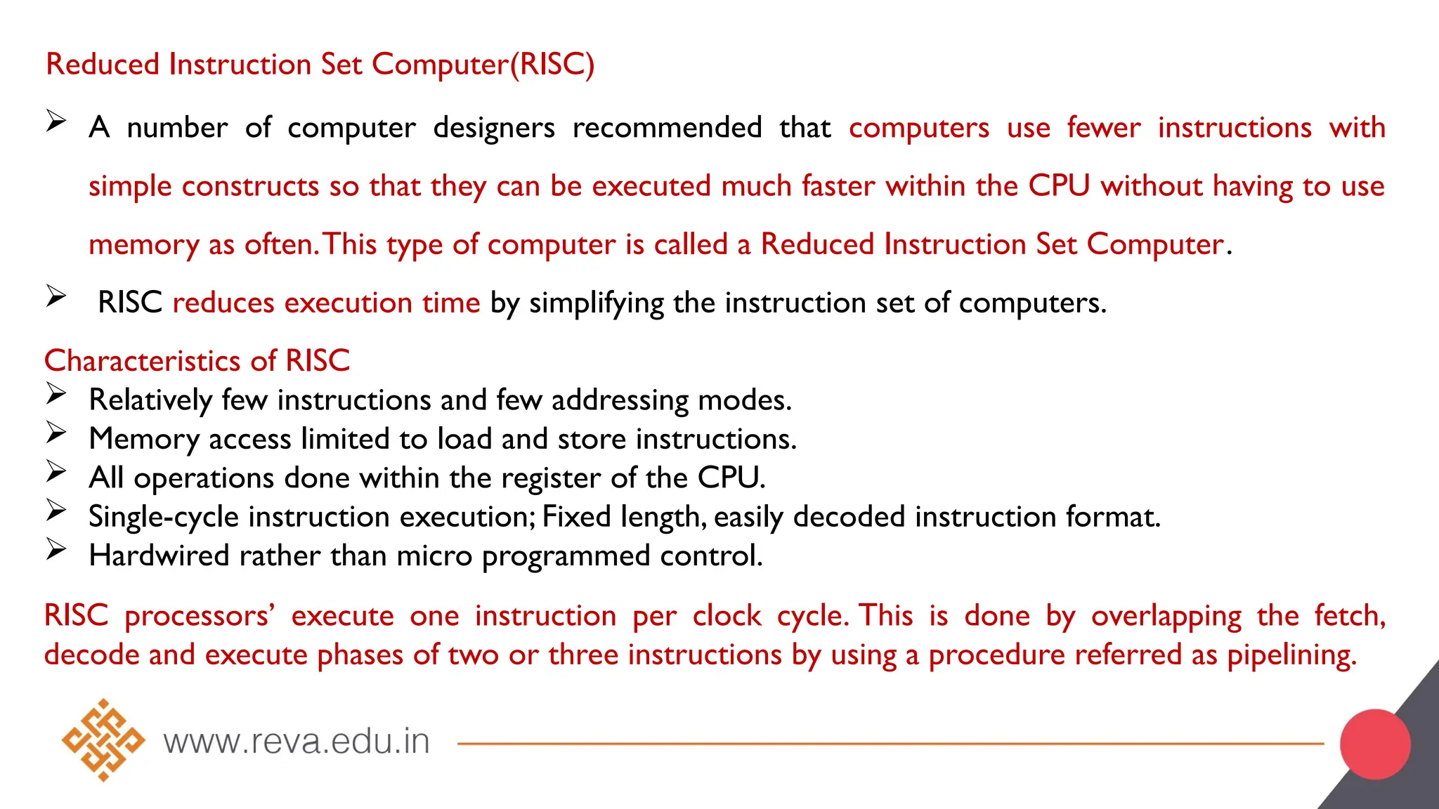
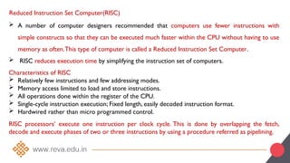
Reduced Instruction SetComputer(RISC)
A number of computer designers recommended that computers use fewer instructions with
simple constructs so that they can be executed much faster within the CPU without having to use
memory as often.This type of computer is called a Reduced Instruction Set Computer.
RISC reduces execution time by simplifying the instruction set of computers.
Characteristics of RISC
Relatively few instructions and few addressing modes.
Memory access limited to load and store instructions.
All operations done within the register of the CPU.
Single-cycle instruction execution; Fixed length, easily decoded instruction format.
Hardwired rather than micro programmed control.
RISC processors’ execute one instruction per clock cycle. This is done by overlapping the fetch,
decode and execute phases of two or three instructions by using a procedure referred as pipelining.
75.
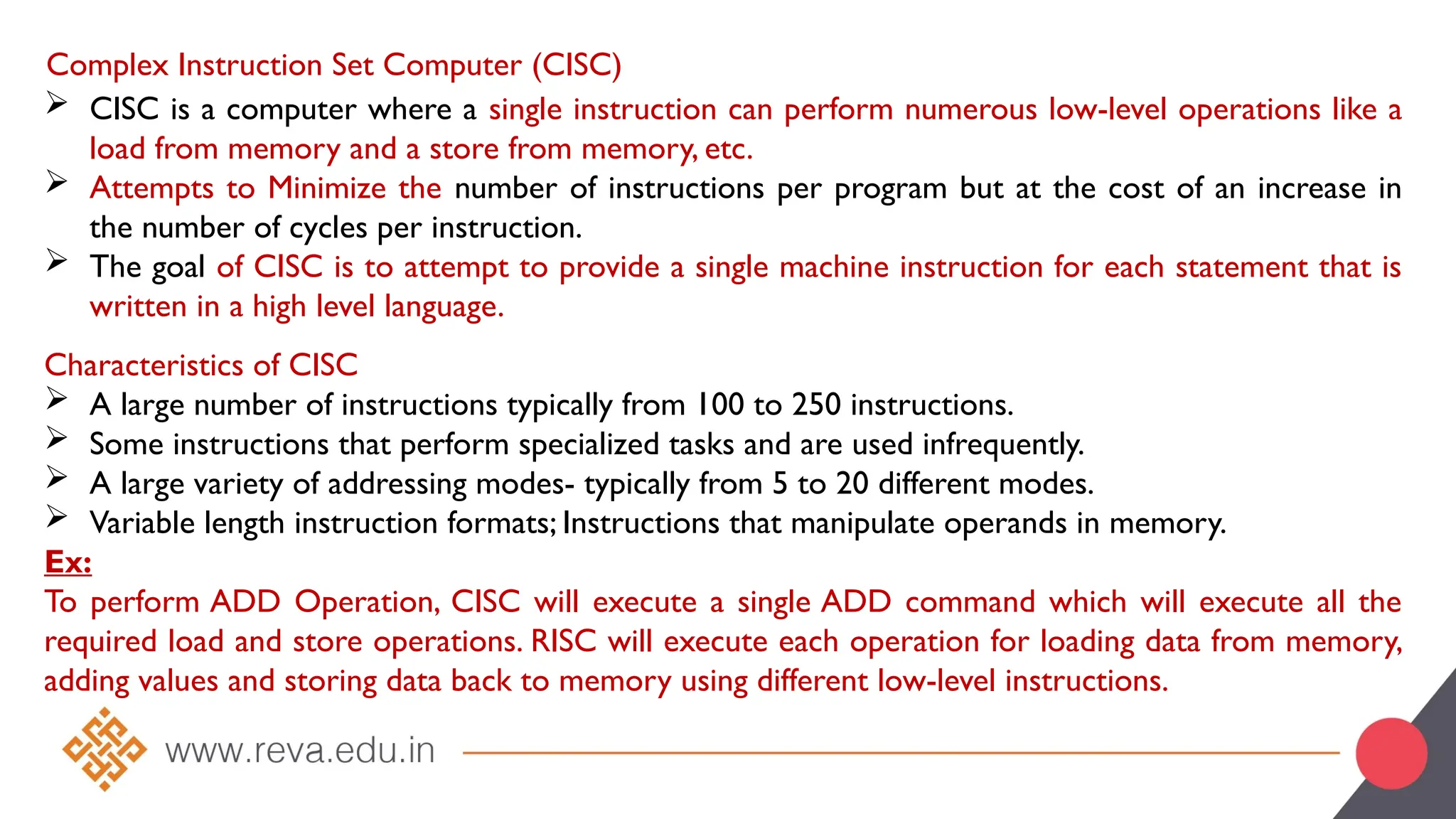
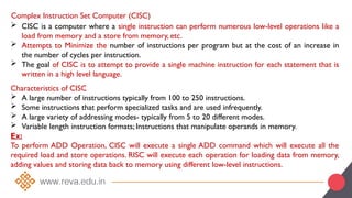
Complex Instruction SetComputer (CISC)
CISC is a computer where a single instruction can perform numerous low-level operations like a
load from memory and a store from memory, etc.
Attempts to Minimize the number of instructions per program but at the cost of an increase in
the number of cycles per instruction.
The goal of CISC is to attempt to provide a single machine instruction for each statement that is
written in a high level language.
Characteristics of CISC
A large number of instructions typically from 100 to 250 instructions.
Some instructions that perform specialized tasks and are used infrequently.
A large variety of addressing modes- typically from 5 to 20 different modes.
Variable length instruction formats; Instructions that manipulate operands in memory.
Ex:
To perform ADD Operation, CISC will execute a single ADD command which will execute all the
required load and store operations. RISC will execute each operation for loading data from memory,
adding values and storing data back to memory using different low-level instructions.
76.
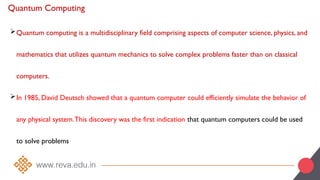
Quantum Computing
Quantum computingis a multidisciplinary field comprising aspects of computer science, physics, and
mathematics that utilizes quantum mechanics to solve complex problems faster than on classical
computers.
In 1985, David Deutsch showed that a quantum computer could efficiently simulate the behavior of
any physical system.This discovery was the first indication that quantum computers could be used
to solve problems
77.
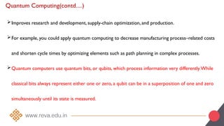
Quantum Computing(contd…)
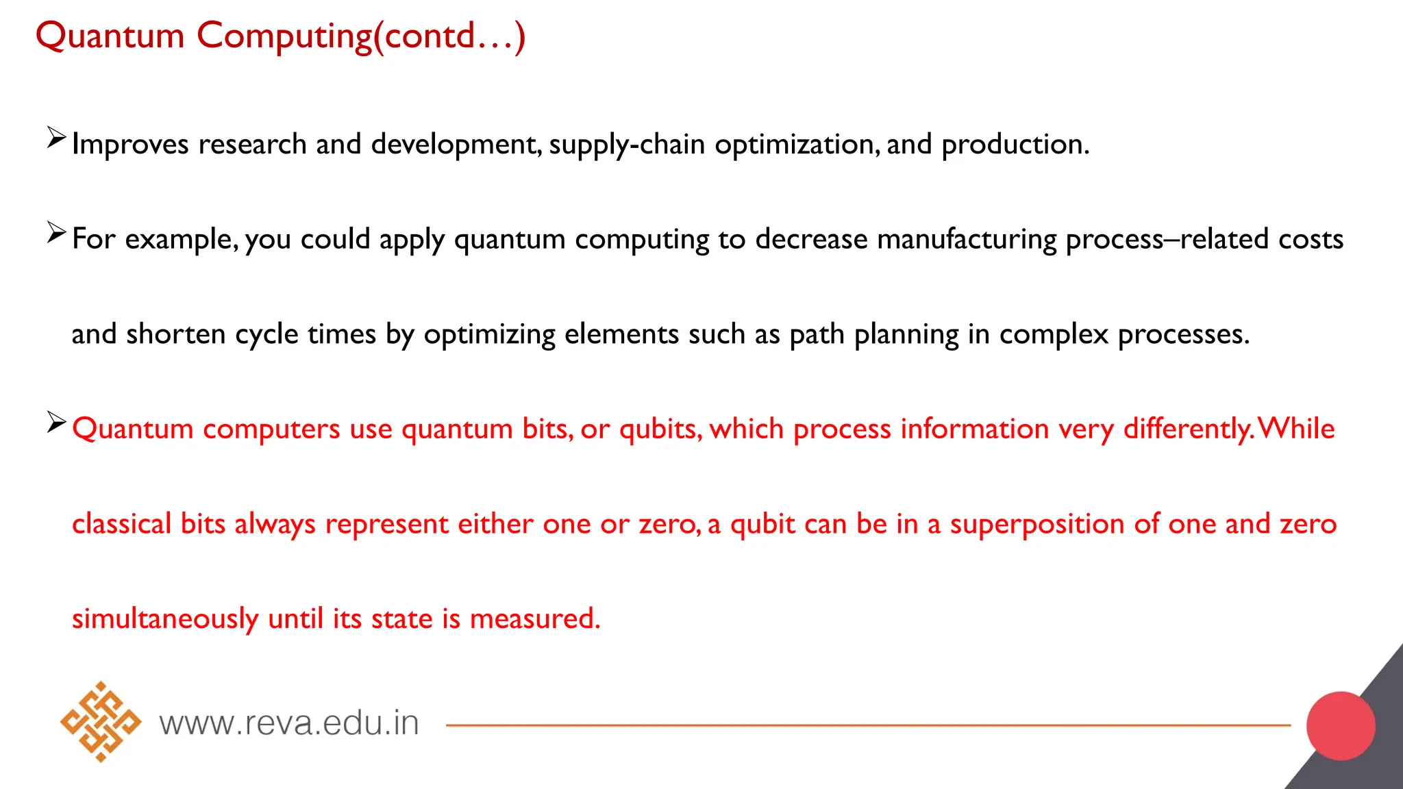
Improves researchand development, supply-chain optimization, and production.
For example, you could apply quantum computing to decrease manufacturing process–related costs
and shorten cycle times by optimizing elements such as path planning in complex processes.
Quantum computers use quantum bits, or qubits, which process information very differently.While
classical bits always represent either one or zero, a qubit can be in a superposition of one and zero
simultaneously until its state is measured.
78.
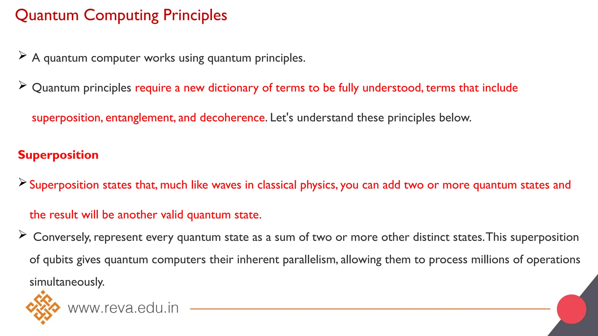
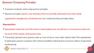
Quantum Computing Principles
A quantum computer works using quantum principles.
Quantum principles require a new dictionary of terms to be fully understood, terms that include
superposition, entanglement, and decoherence. Let's understand these principles below.
Superposition
Superposition states that, much like waves in classical physics, you can add two or more quantum states and
the result will be another valid quantum state.
Conversely, represent every quantum state as a sum of two or more other distinct states.This superposition
of qubits gives quantum computers their inherent parallelism, allowing them to process millions of operations
simultaneously.
79.
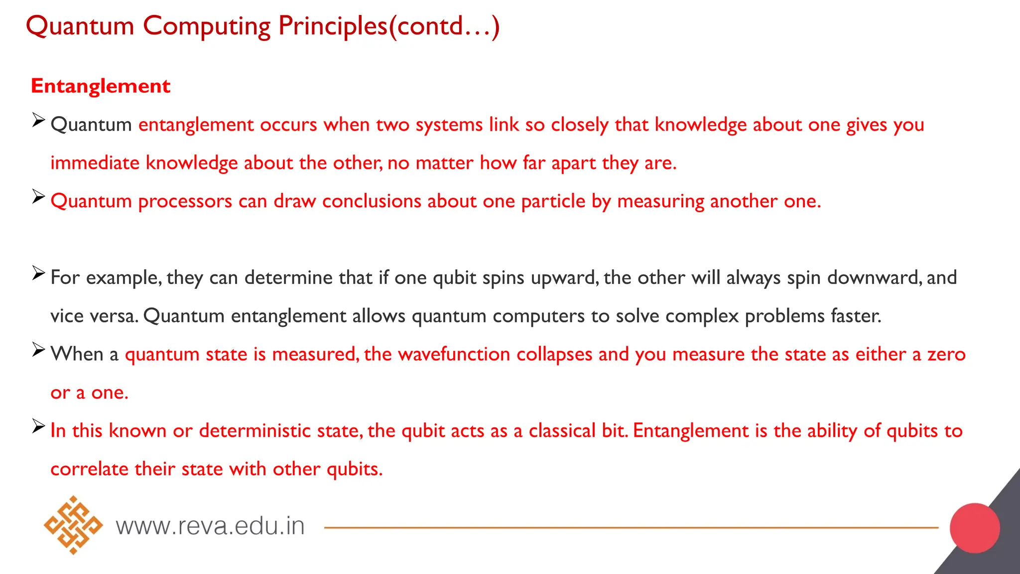
Quantum Computing Principles(contd…)
Entanglement
Quantumentanglement occurs when two systems link so closely that knowledge about one gives you
immediate knowledge about the other, no matter how far apart they are.
Quantum processors can draw conclusions about one particle by measuring another one.
For example, they can determine that if one qubit spins upward, the other will always spin downward, and
vice versa. Quantum entanglement allows quantum computers to solve complex problems faster.
When a quantum state is measured, the wavefunction collapses and you measure the state as either a zero
or a one.
In this known or deterministic state, the qubit acts as a classical bit. Entanglement is the ability of qubits to
correlate their state with other qubits.
80.
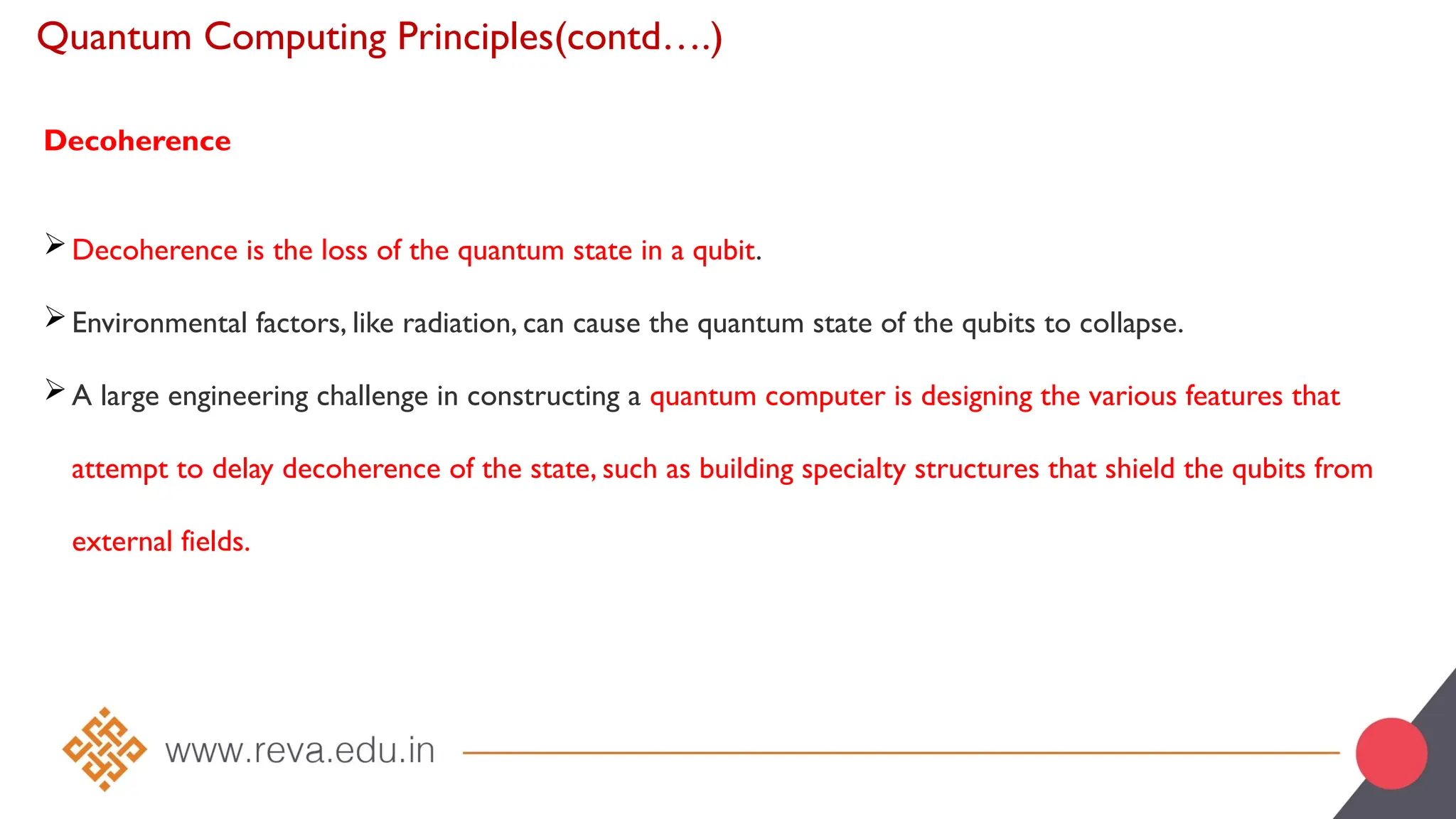
Quantum Computing Principles(contd….)
Decoherence
Decoherenceis the loss of the quantum state in a qubit.
Environmental factors, like radiation, can cause the quantum state of the qubits to collapse.
A large engineering challenge in constructing a quantum computer is designing the various features that
attempt to delay decoherence of the state, such as building specialty structures that shield the qubits from
external fields.
81.
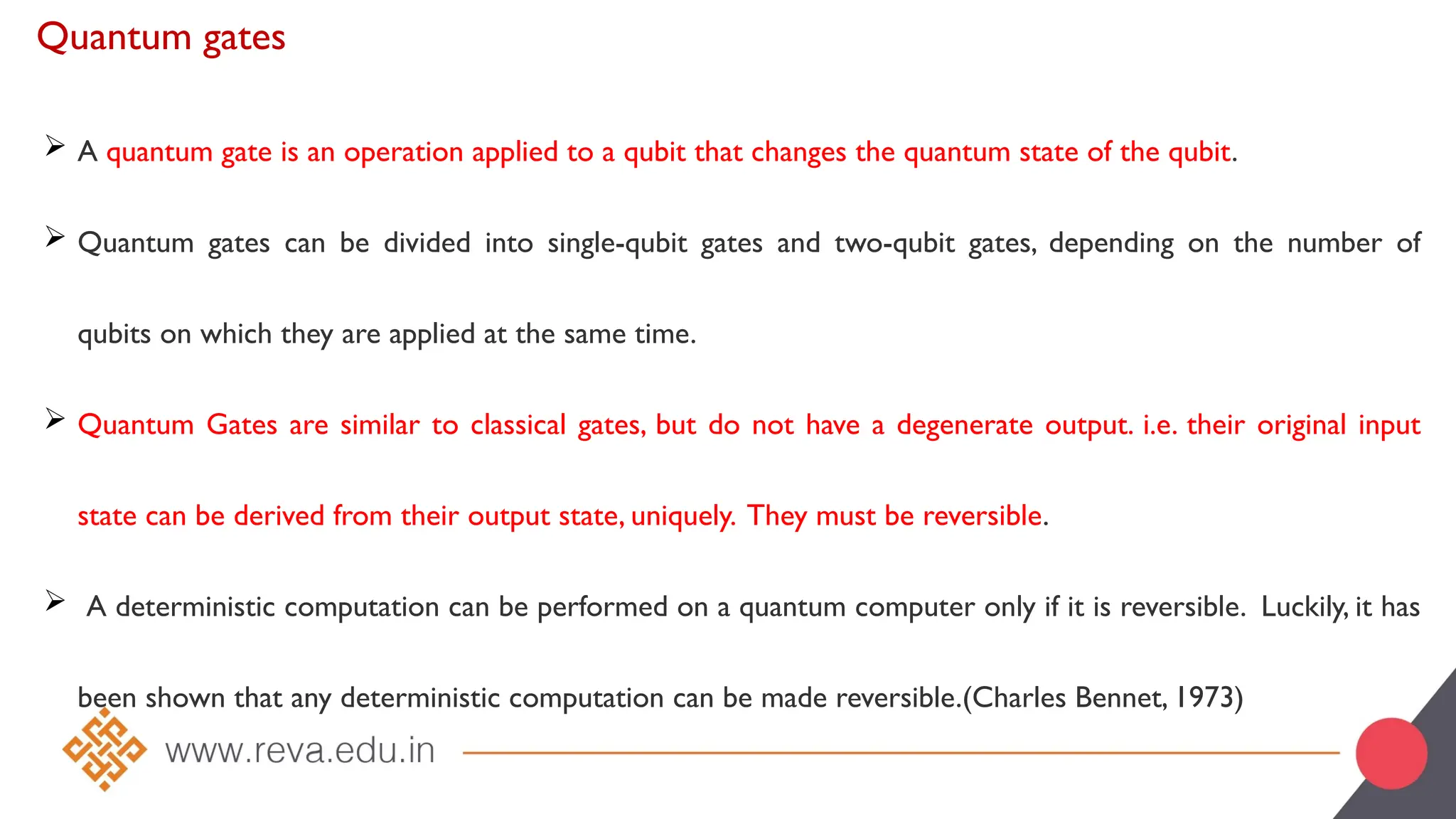
Quantum gates
Aquantum gate is an operation applied to a qubit that changes the quantum state of the qubit.
Quantum gates can be divided into single-qubit gates and two-qubit gates, depending on the number of
qubits on which they are applied at the same time.
Quantum Gates are similar to classical gates, but do not have a degenerate output. i.e. their original input
state can be derived from their output state, uniquely. They must be reversible.
A deterministic computation can be performed on a quantum computer only if it is reversible. Luckily, it has
been shown that any deterministic computation can be made reversible.(Charles Bennet, 1973)
82.
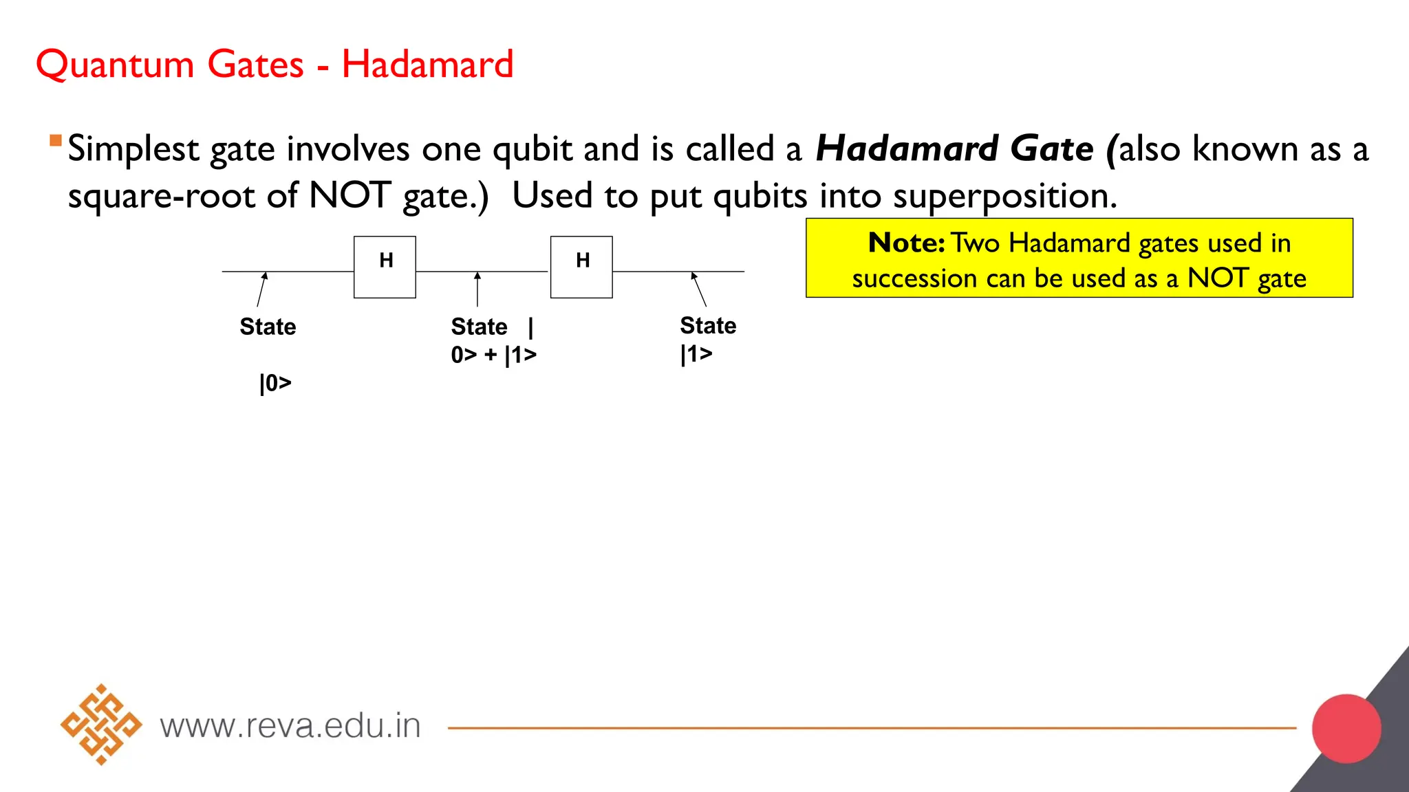
Quantum Gates -Hadamard
Simplest gate involves one qubit and is called a Hadamard Gate (also known as a
square-root of NOT gate.) Used to put qubits into superposition.
H
State
|0>
State |
0> + |1>
H
State
|1>
Note: Two Hadamard gates used in
succession can be used as a NOT gate
83.
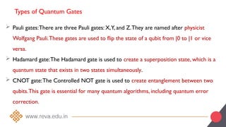
Types of QuantumGates
Pauli gates:There are three Pauli gates: X,Y, and Z.They are named after physicist
Wolfgang Pauli.These gates are used to flip the state of a qubit from |0 to |1 or vice
versa.
Hadamard gate:The Hadamard gate is used to create a superposition state, which is a
quantum state that exists in two states simultaneously.
CNOT gate:The Controlled NOT gate is used to create entanglement between two
qubits.This gate is essential for many quantum algorithms, including quantum error
correction.
84.
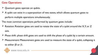
Gate Operations
Quantumgates operate on qubits.
A qubit can exist in a superposition of two states, which allows quantum gates to
perform multiple operations simultaneously.
The most common operations performed by quantum gates include:
Rotation: Rotation gates are used to rotate the state of a qubit around the X,Y, or Z
axis.
Phase shift: phase shift gates are used to shift the phase of a qubit by a certain amount.
Measurement: Measurement gates are used to measure the state of a qubit, collapsing it
to either |0 or |1.
85.
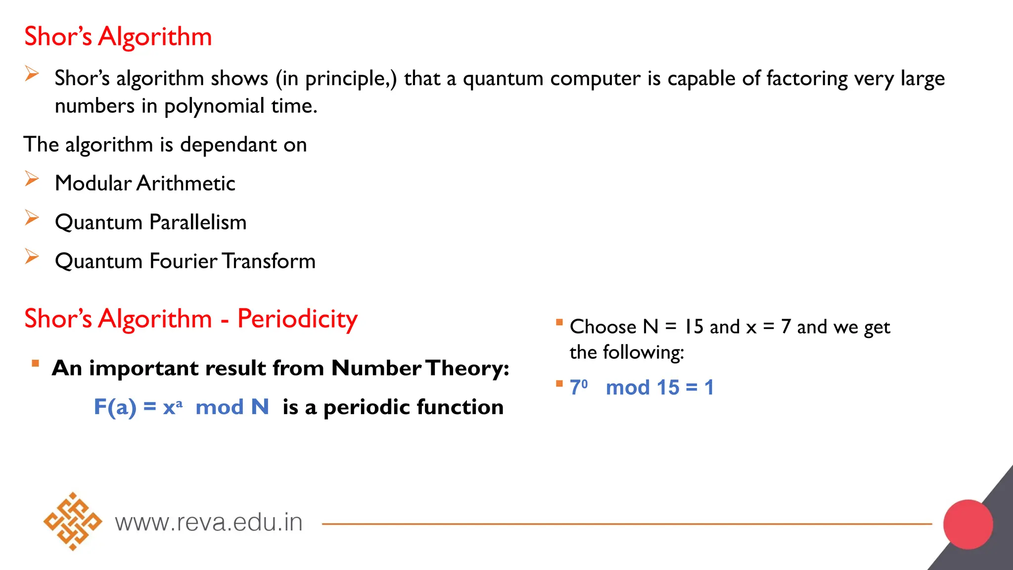
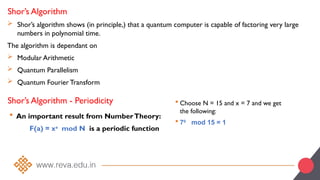
Shor’s Algorithm
Shor’salgorithm shows (in principle,) that a quantum computer is capable of factoring very large
numbers in polynomial time.
The algorithm is dependant on
Modular Arithmetic
Quantum Parallelism
Quantum Fourier Transform
Shor’s Algorithm - Periodicity
An important result from NumberTheory:
F(a) = xa
mod N is a periodic function
Choose N = 15 and x = 7 and we get
the following:
70
mod 15 = 1
86.
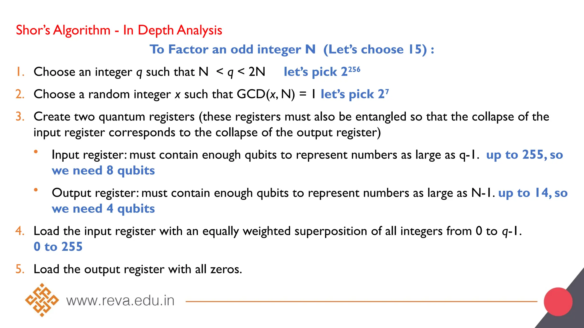
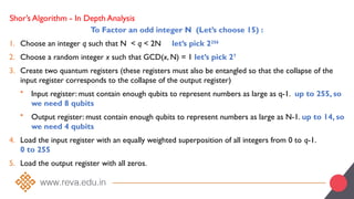
Shor’s Algorithm -In Depth Analysis
To Factor an odd integer N (Let’s choose 15) :
1. Choose an integer q such that N < q < 2N let’s pick 2256
2. Choose a random integer x such that GCD(x, N) = 1 let’s pick 27
3. Create two quantum registers (these registers must also be entangled so that the collapse of the
input register corresponds to the collapse of the output register)
• Input register: must contain enough qubits to represent numbers as large as q-1. up to 255, so
we need 8 qubits
• Output register: must contain enough qubits to represent numbers as large as N-1. up to 14, so
we need 4 qubits
4. Load the input register with an equally weighted superposition of all integers from 0 to q-1.
0 to 255
5. Load the output register with all zeros.
87.
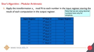
Shor’s Algorithm -Modular Arithmetic
6. Apply the transformation xa mod N to each number in the input register, storing the
result of each computation in the output register.
Input Register 7 Mod 15 Output Register
|0> 7 Mod 15 1
|1> 7 Mod 15 7
|2> 7 Mod 15 4
|3> 7 Mod 15 13
|4> 7 Mod 15 1
|5> 7 Mod 15 7
|6> 7 Mod 15 4
|7> 7 Mod 15 13
a
0
1
6
5
4
3
2
Note that we are using decimal
numbers here only for
simplicity.
88.
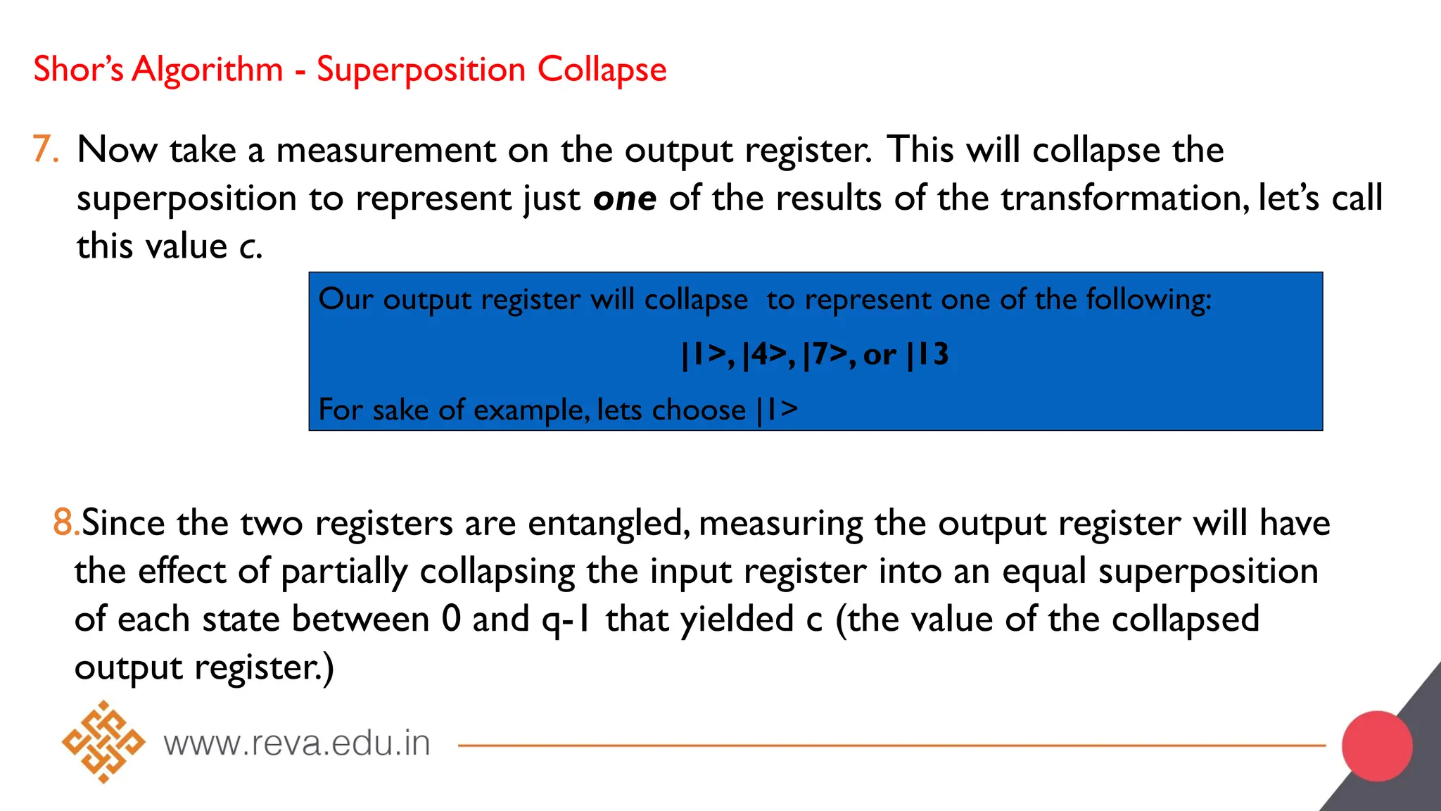
Shor’s Algorithm -Superposition Collapse
7. Now take a measurement on the output register. This will collapse the
superposition to represent just one of the results of the transformation, let’s call
this value c.
Our output register will collapse to represent one of the following:
|1>, |4>, |7>, or |13
For sake of example, lets choose |1>
8.Since the two registers are entangled, measuring the output register will have
the effect of partially collapsing the input register into an equal superposition
of each state between 0 and q-1 that yielded c (the value of the collapsed
output register.)
89.
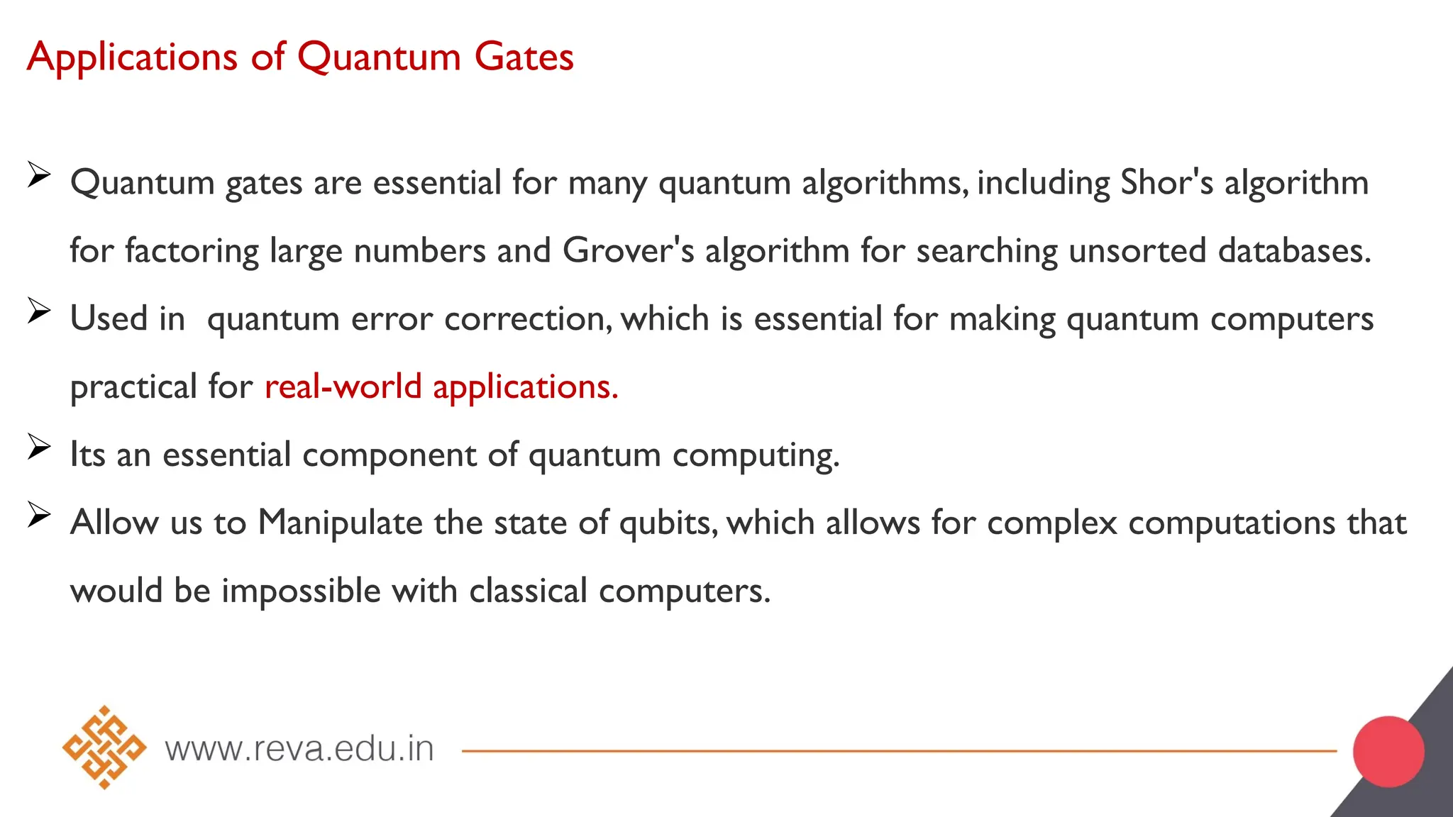
Applications of QuantumGates
Quantum gates are essential for many quantum algorithms, including Shor's algorithm
for factoring large numbers and Grover's algorithm for searching unsorted databases.
Used in quantum error correction, which is essential for making quantum computers
practical for real-world applications.
Its an essential component of quantum computing.
Allow us to Manipulate the state of qubits, which allows for complex computations that
would be impossible with classical computers.


![INSTRUCTION FORMATS
● Three-Address Instructions
● ADD R1, R2, R3 R1 R2 + R3
←
● Two-Address Instructions
● ADD R1, R2 R1 R1 + R2
←
● One-Address Instructions
● ADD M AC AC + M[AR]
←
Zero-Address Instructions
● ADD TOS TOS + (TOS – 1)
←
RISC Instructions
● Lots of registers. Memory is restricted to Load & Store
●
Opcode Operand(s) or Address(es)](https://image.slidesharecdn.com/b23da010104new1-250925153402-7ed593fd/85/Digital-logic-and-computer-design-with-Unit-2-topics-67-320.jpg)
![INSTRUCTION FORMATS
Example: Evaluate (A+B) * (C+D)
● Three-Address
l ADD R1, A, B
ADD R2, C, D
MUL X, R1, R2
; R1 ← M[A] + M[B]
; R2 ← M[C] + M[D]
; M[X] ← R1 * R2
l
l](https://image.slidesharecdn.com/b23da010104new1-250925153402-7ed593fd/85/Digital-logic-and-computer-design-with-Unit-2-topics-68-320.jpg)
![INSTRUCTION FORMATS
Example: Evaluate (A+B) * (C+D)
●
Two-Address
l
MOVR1, A
ADD R1, B
MOVR2, C
ADD R2, D
MUL R1, R2
MOVX, R1
; R1 ← M[A]
; R1 ← R1 + M[B]
; R2 ← M[C]
; R2 ← R2 + M[D]
; R1 ← R1 * R2
; M[X] ← R1
l
l
l
l
l](https://image.slidesharecdn.com/b23da010104new1-250925153402-7ed593fd/85/Digital-logic-and-computer-design-with-Unit-2-topics-69-320.jpg)
![INSTRUCTION FORMATS
Example: Evaluate (A+B) * (C+D)
● One-Address
l LOAD A
ADD B
; AC ← M[A]
; AC ← AC + M[B]
; M[T] ← AC
; AC ← M[C]
; AC ← AC + M[D]
; AC ← AC * M[T]
; M[X] ← AC
l
l STORET
l LOAD C
ADD D
MUL T
l
l
l STOREX](https://image.slidesharecdn.com/b23da010104new1-250925153402-7ed593fd/85/Digital-logic-and-computer-design-with-Unit-2-topics-70-320.jpg)
![INSTRUCTION FORMATS
Example: Evaluate (A+B) * (C+D)
●
Zero-Address
l
PUSH A
PUSH B
ADD PUSH
C
PUSH D
ADD
;TOS A
←
;TOS B
←
;TOS (A + B)
←
;TOS C
←
;TOS D
←
;TOS (C + D)
←
;TOS ←
l
l
l
l
l
l
MUL (C+D)*(A+B)
POP X
l
; M[X] TOS
←](https://image.slidesharecdn.com/b23da010104new1-250925153402-7ed593fd/85/Digital-logic-and-computer-design-with-Unit-2-topics-71-320.jpg)


![INSTRUCTION FORMATS
● Three-Address Instructions
● ADD R1, R2, R3 R1 R2 + R3
←
● Two-Address Instructions
● ADD R1, R2 R1 R1 + R2
←
● One-Address Instructions
● ADD M AC AC + M[AR]
←
Zero-Address Instructions
● ADD TOS TOS + (TOS – 1)
←
RISC Instructions
● Lots of registers. Memory is restricted to Load & Store
●
Opcode Operand(s) or Address(es)](https://image.slidesharecdn.com/b23da010104new1-250925153402-7ed593fd/75/Digital-logic-and-computer-design-with-Unit-2-topics-67-2048.jpg)
![INSTRUCTION FORMATS
Example: Evaluate (A+B) * (C+D)
● Three-Address
l ADD R1, A, B
ADD R2, C, D
MUL X, R1, R2
; R1 ← M[A] + M[B]
; R2 ← M[C] + M[D]
; M[X] ← R1 * R2
l
l](https://image.slidesharecdn.com/b23da010104new1-250925153402-7ed593fd/75/Digital-logic-and-computer-design-with-Unit-2-topics-68-2048.jpg)
![INSTRUCTION FORMATS
Example: Evaluate (A+B) * (C+D)
●
Two-Address
l
MOVR1, A
ADD R1, B
MOVR2, C
ADD R2, D
MUL R1, R2
MOVX, R1
; R1 ← M[A]
; R1 ← R1 + M[B]
; R2 ← M[C]
; R2 ← R2 + M[D]
; R1 ← R1 * R2
; M[X] ← R1
l
l
l
l
l](https://image.slidesharecdn.com/b23da010104new1-250925153402-7ed593fd/75/Digital-logic-and-computer-design-with-Unit-2-topics-69-2048.jpg)
![INSTRUCTION FORMATS
Example: Evaluate (A+B) * (C+D)
● One-Address
l LOAD A
ADD B
; AC ← M[A]
; AC ← AC + M[B]
; M[T] ← AC
; AC ← M[C]
; AC ← AC + M[D]
; AC ← AC * M[T]
; M[X] ← AC
l
l STORET
l LOAD C
ADD D
MUL T
l
l
l STOREX](https://image.slidesharecdn.com/b23da010104new1-250925153402-7ed593fd/75/Digital-logic-and-computer-design-with-Unit-2-topics-70-2048.jpg)
![INSTRUCTION FORMATS
Example: Evaluate (A+B) * (C+D)
●
Zero-Address
l
PUSH A
PUSH B
ADD PUSH
C
PUSH D
ADD
;TOS A
←
;TOS B
←
;TOS (A + B)
←
;TOS C
←
;TOS D
←
;TOS (C + D)
←
;TOS ←
l
l
l
l
l
l
MUL (C+D)*(A+B)
POP X
l
; M[X] TOS
←](https://image.slidesharecdn.com/b23da010104new1-250925153402-7ed593fd/75/Digital-logic-and-computer-design-with-Unit-2-topics-71-2048.jpg)