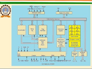
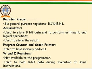
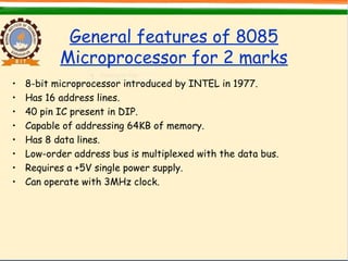
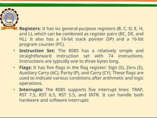
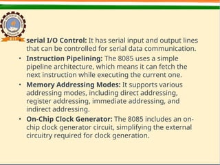
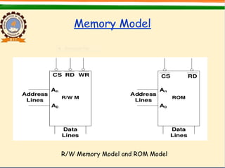
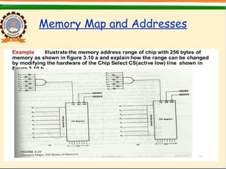
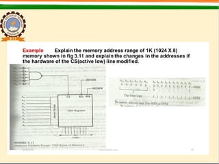
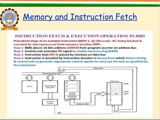
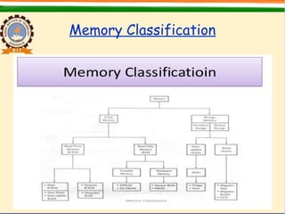
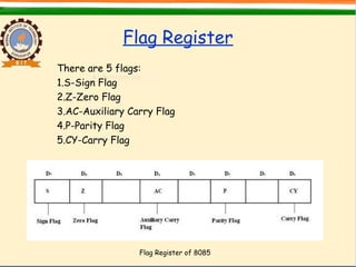
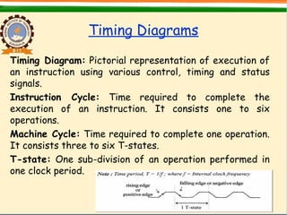
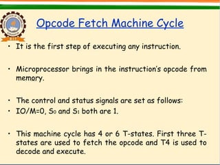
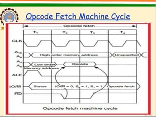
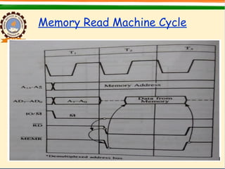
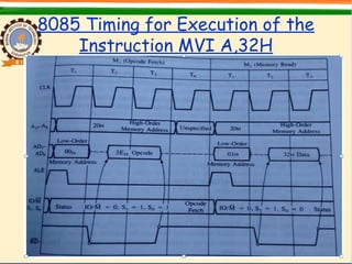
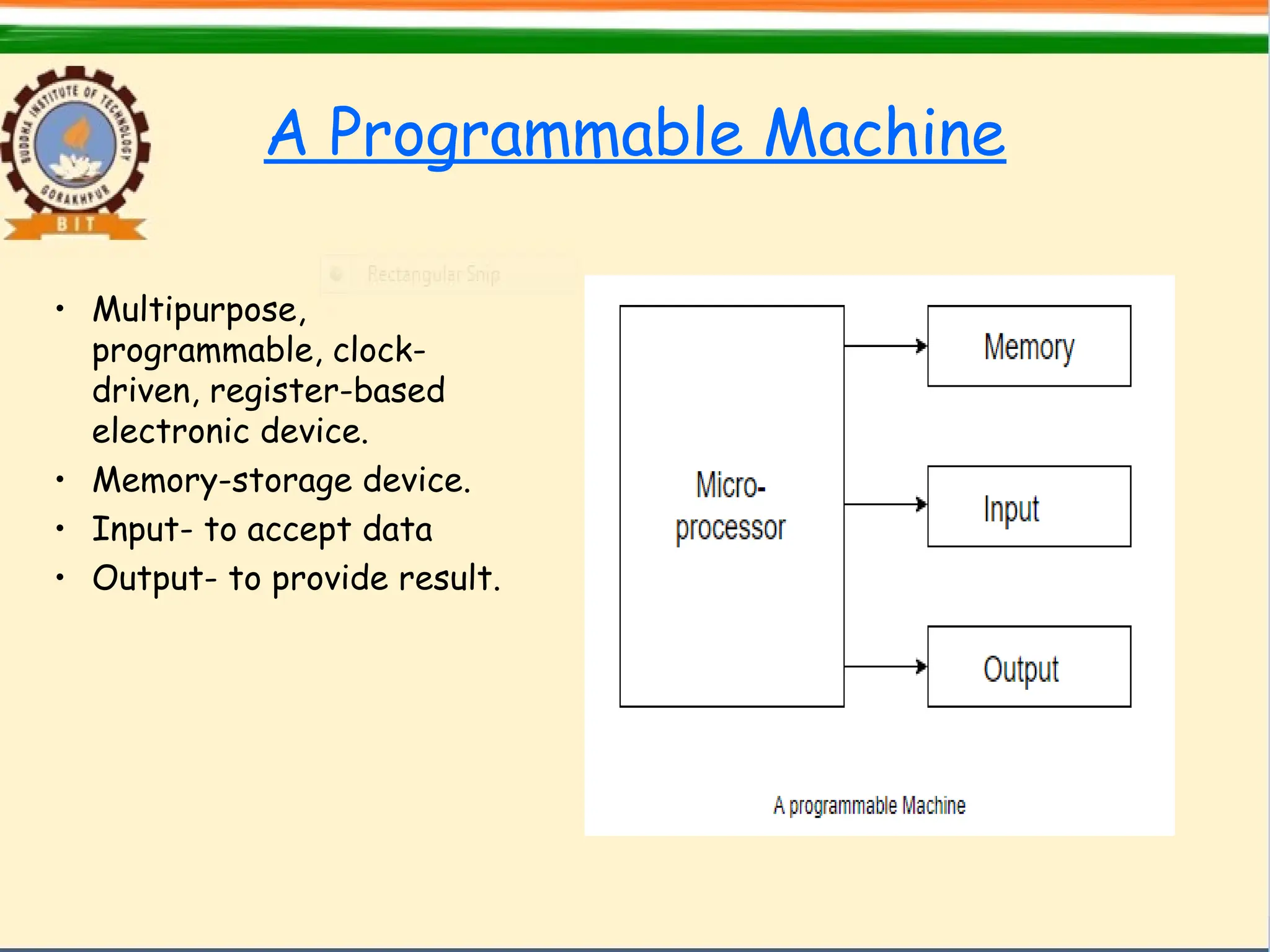
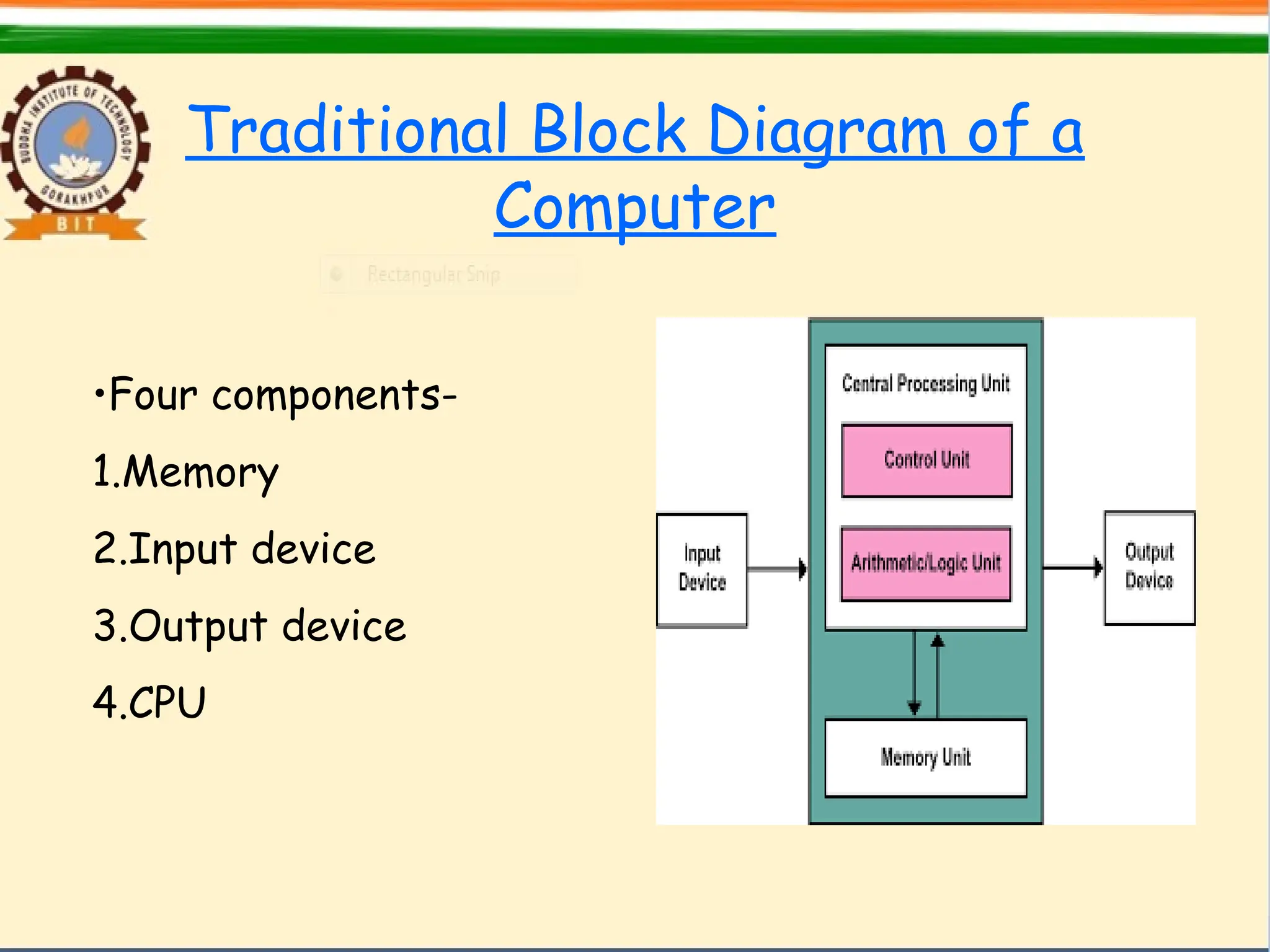
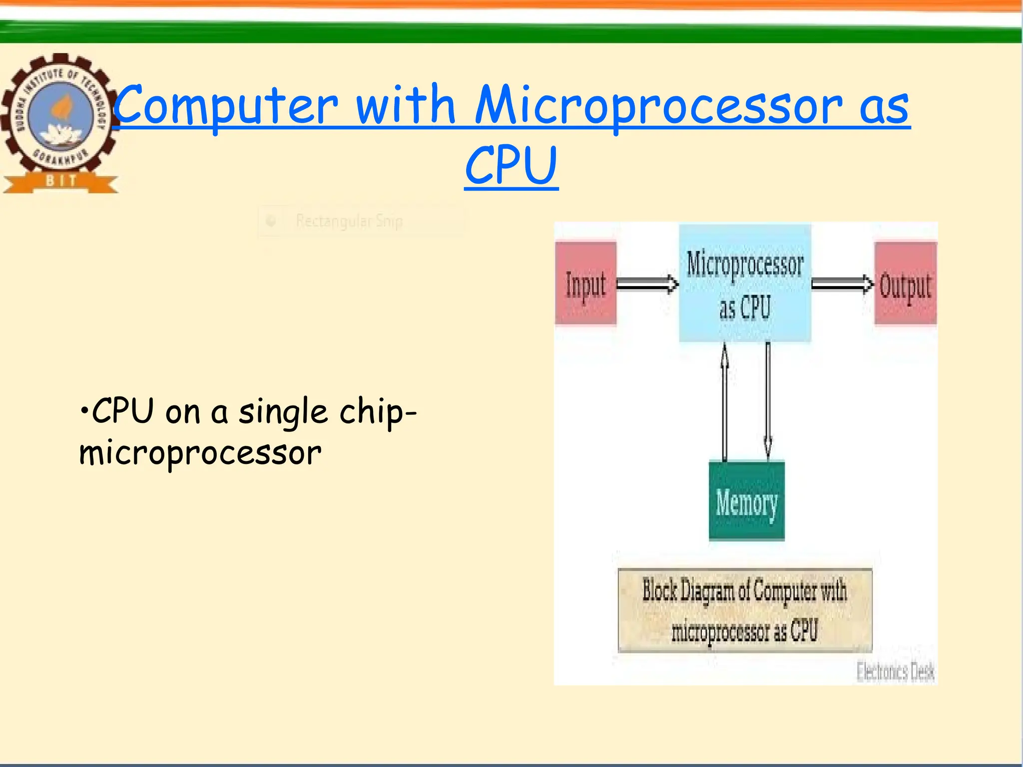
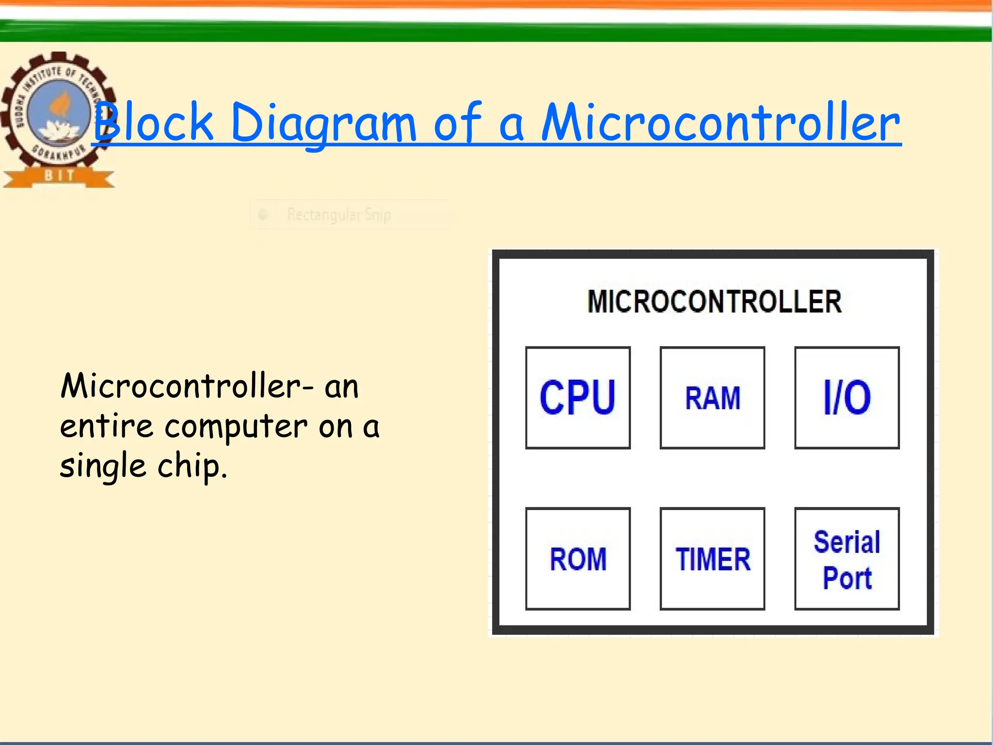
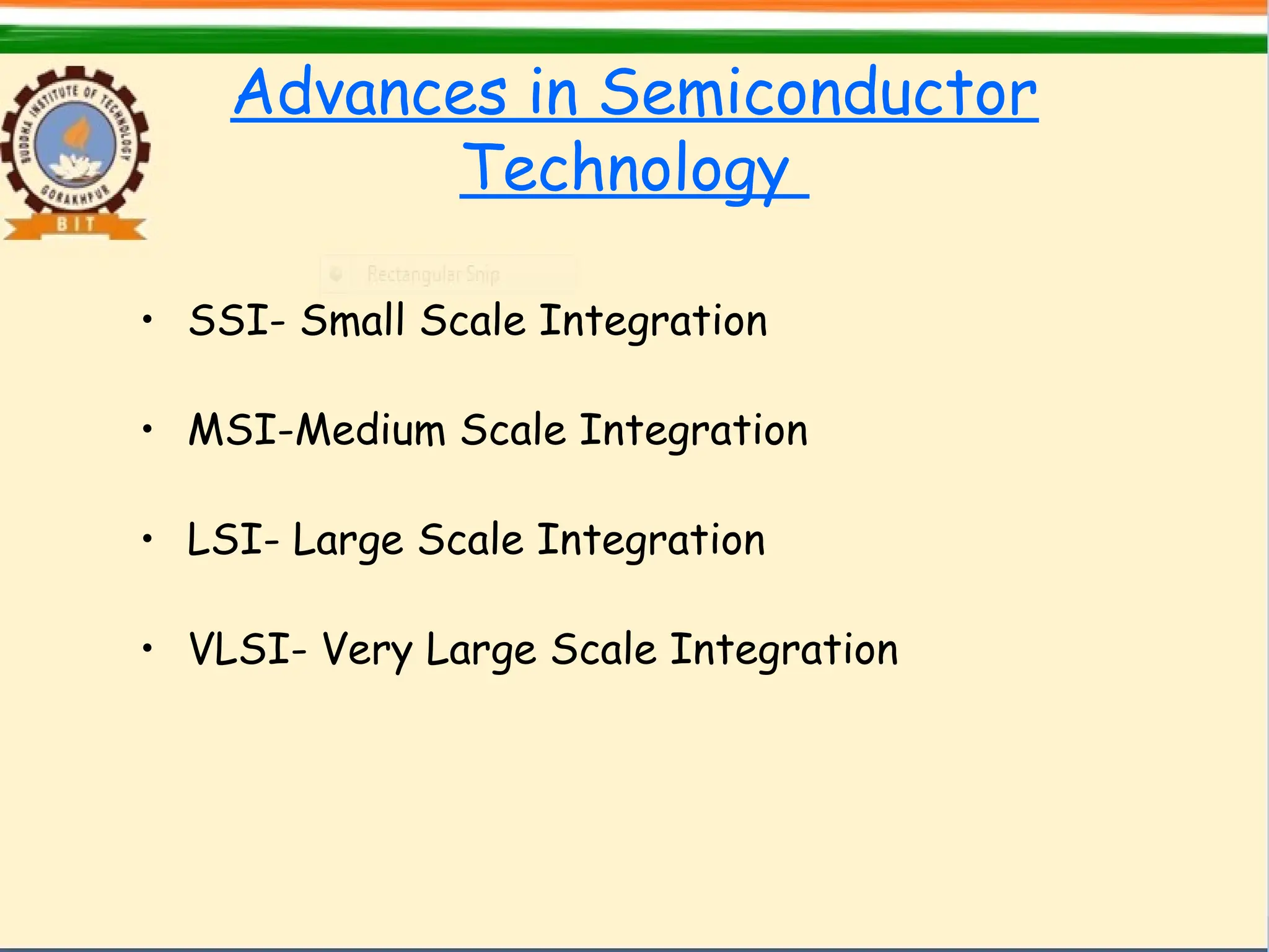
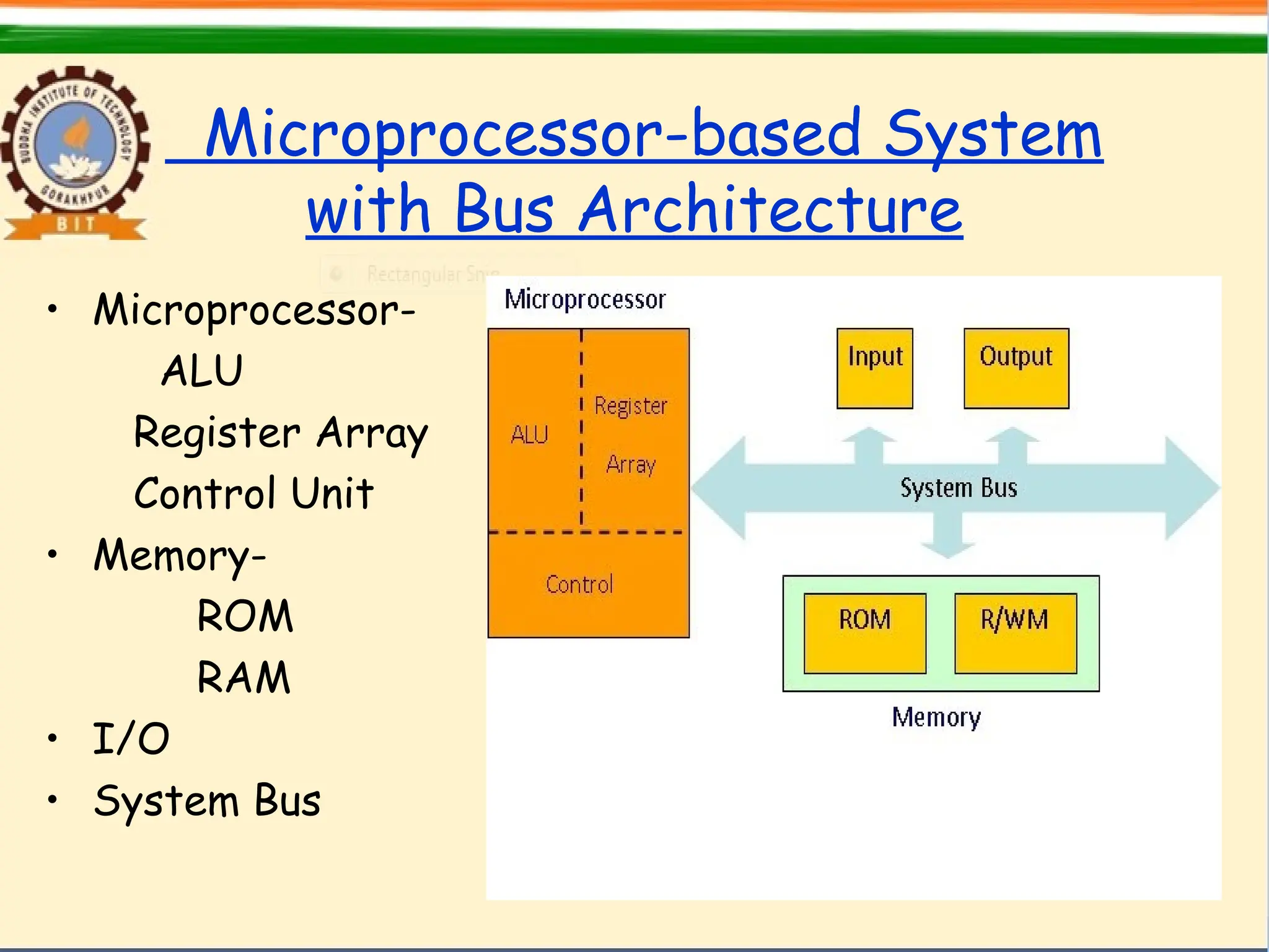
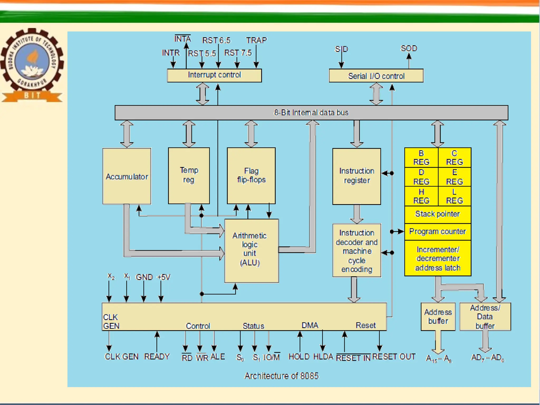
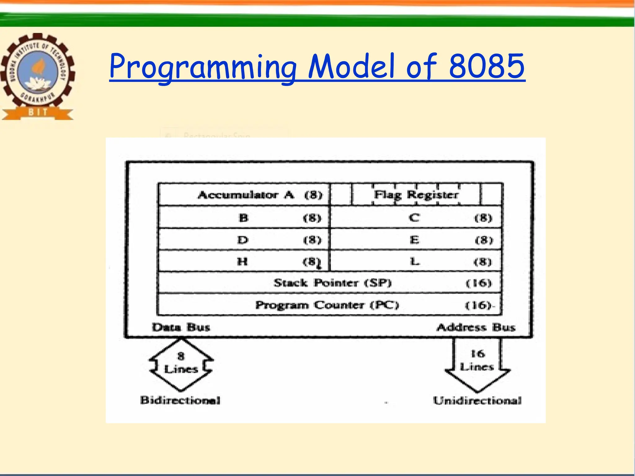
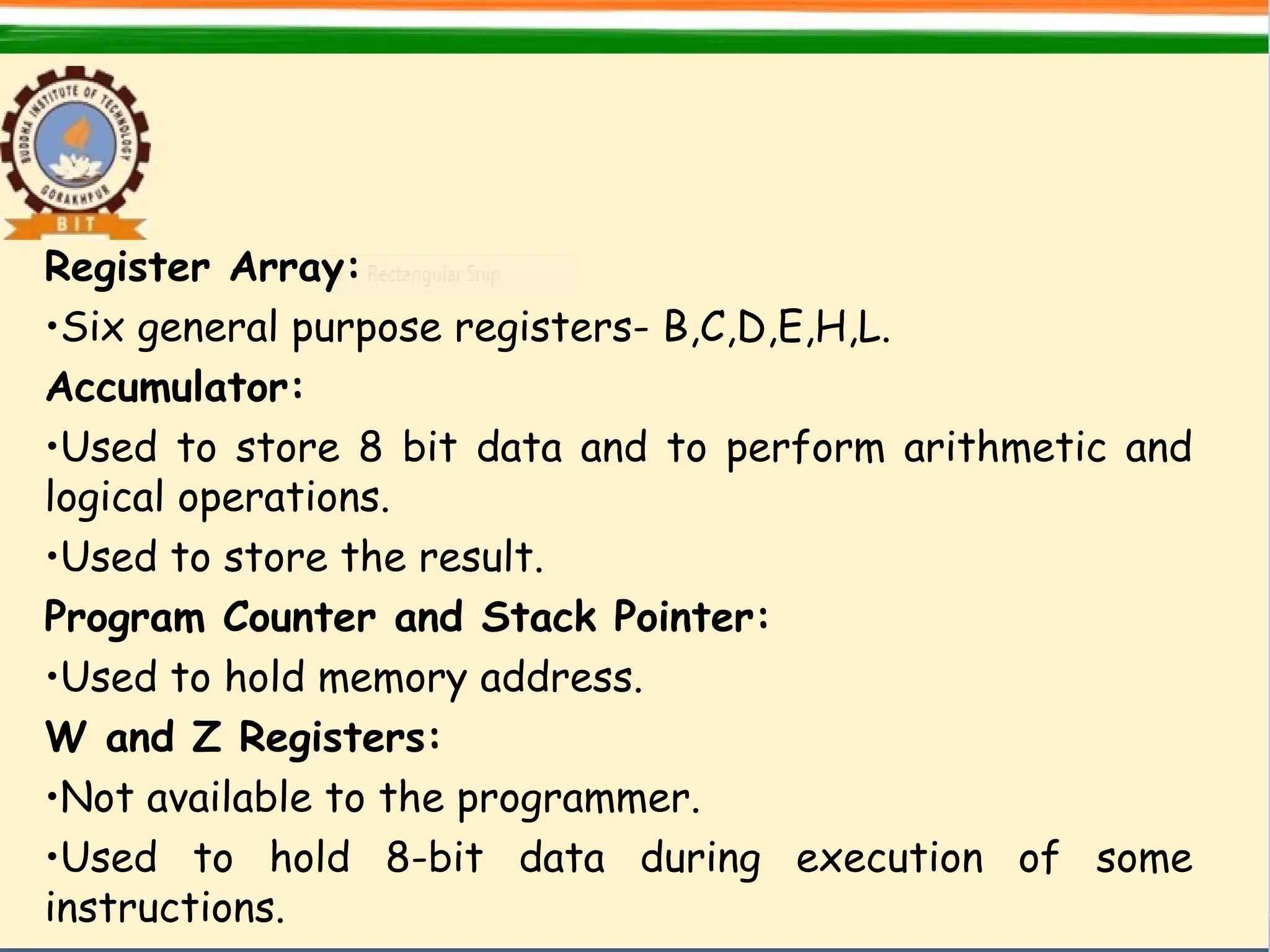
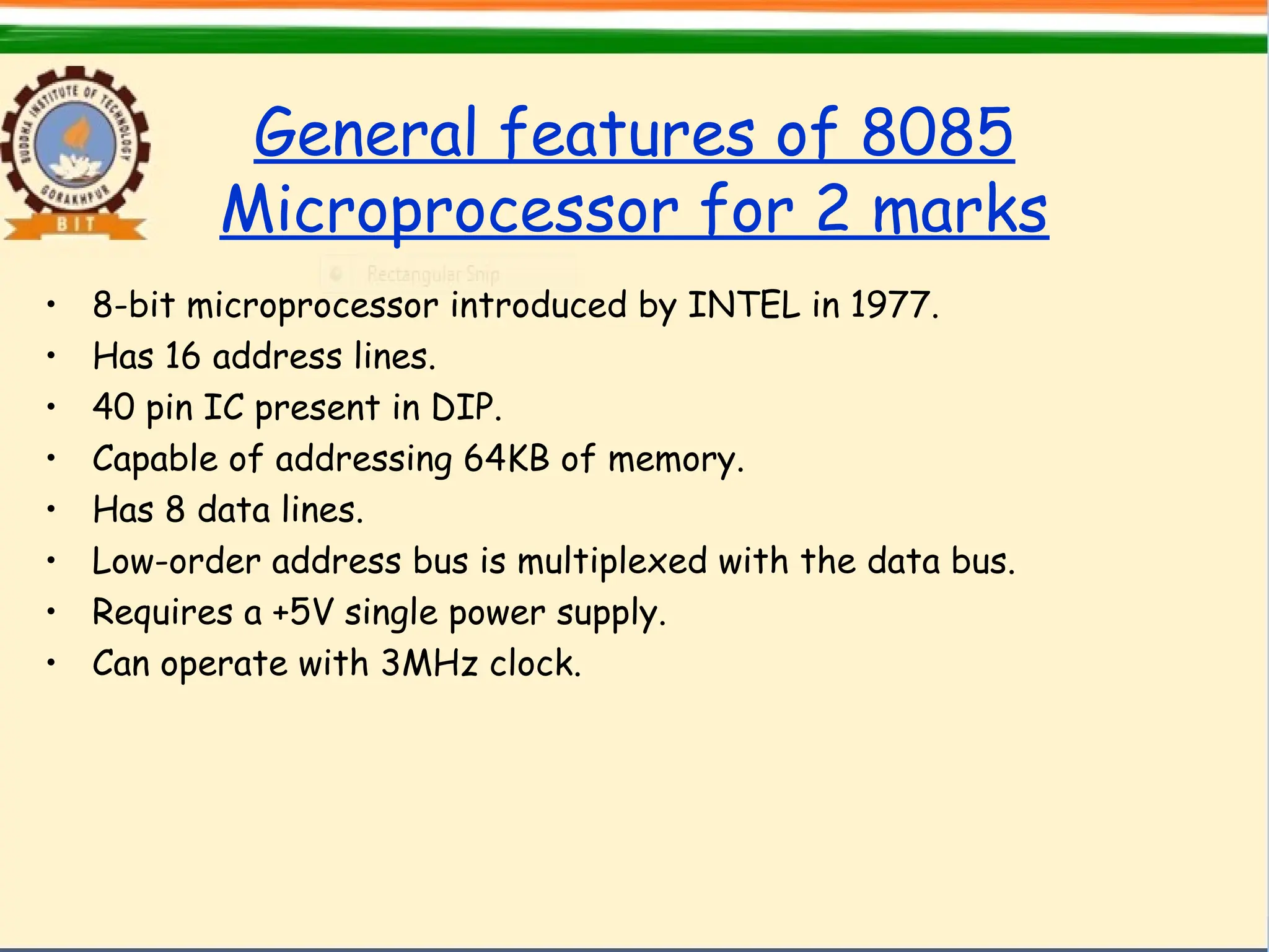
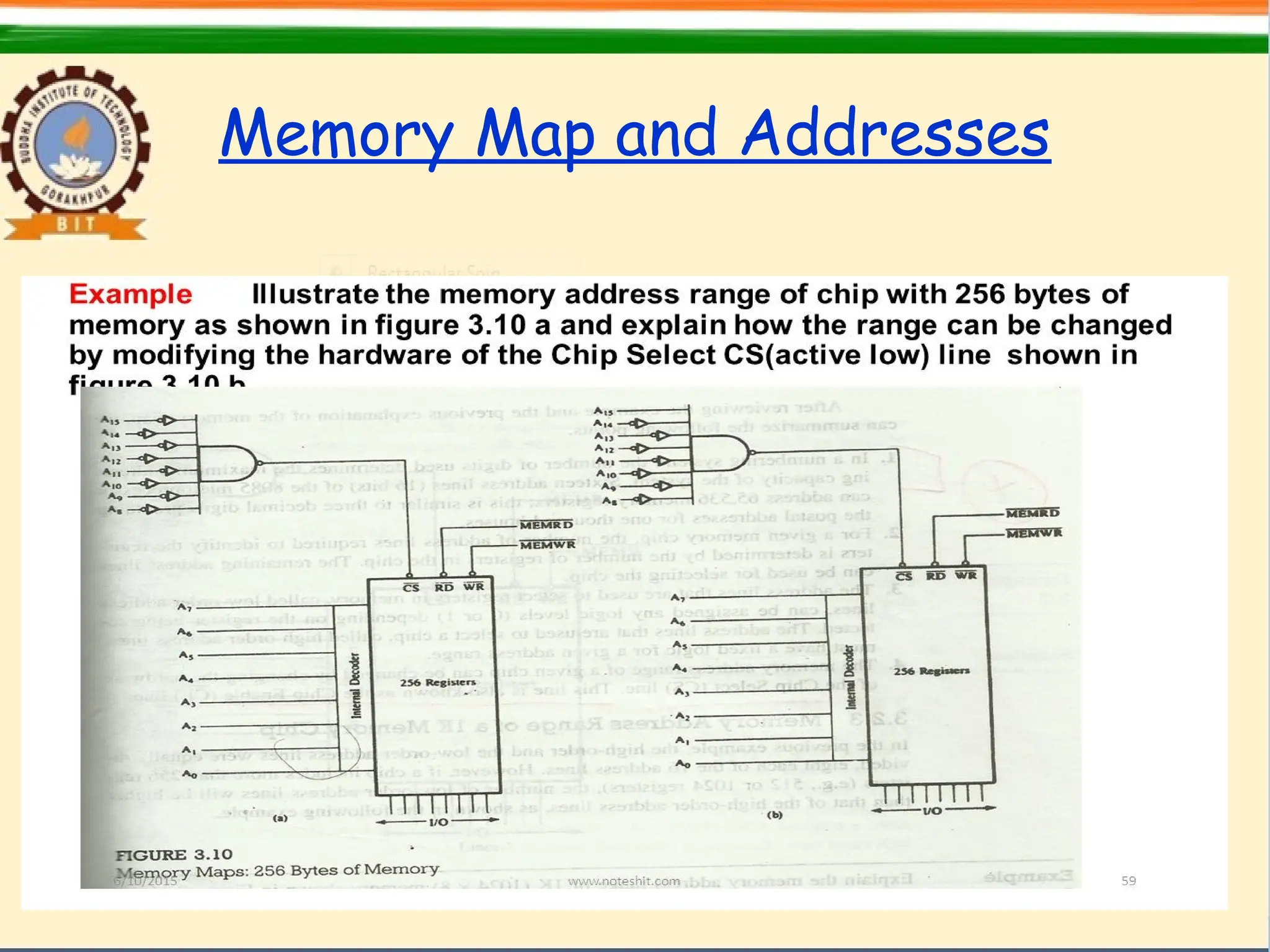
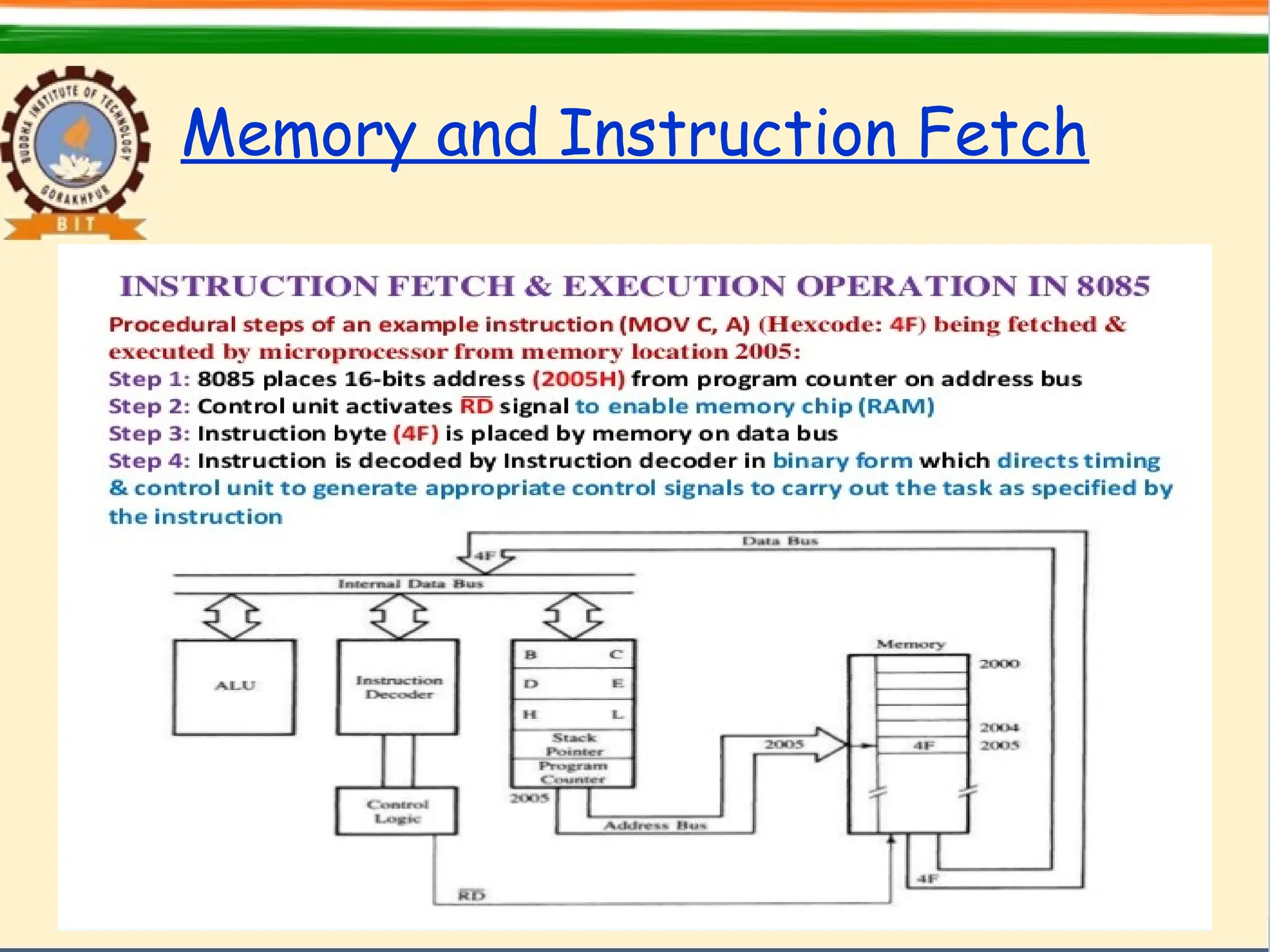
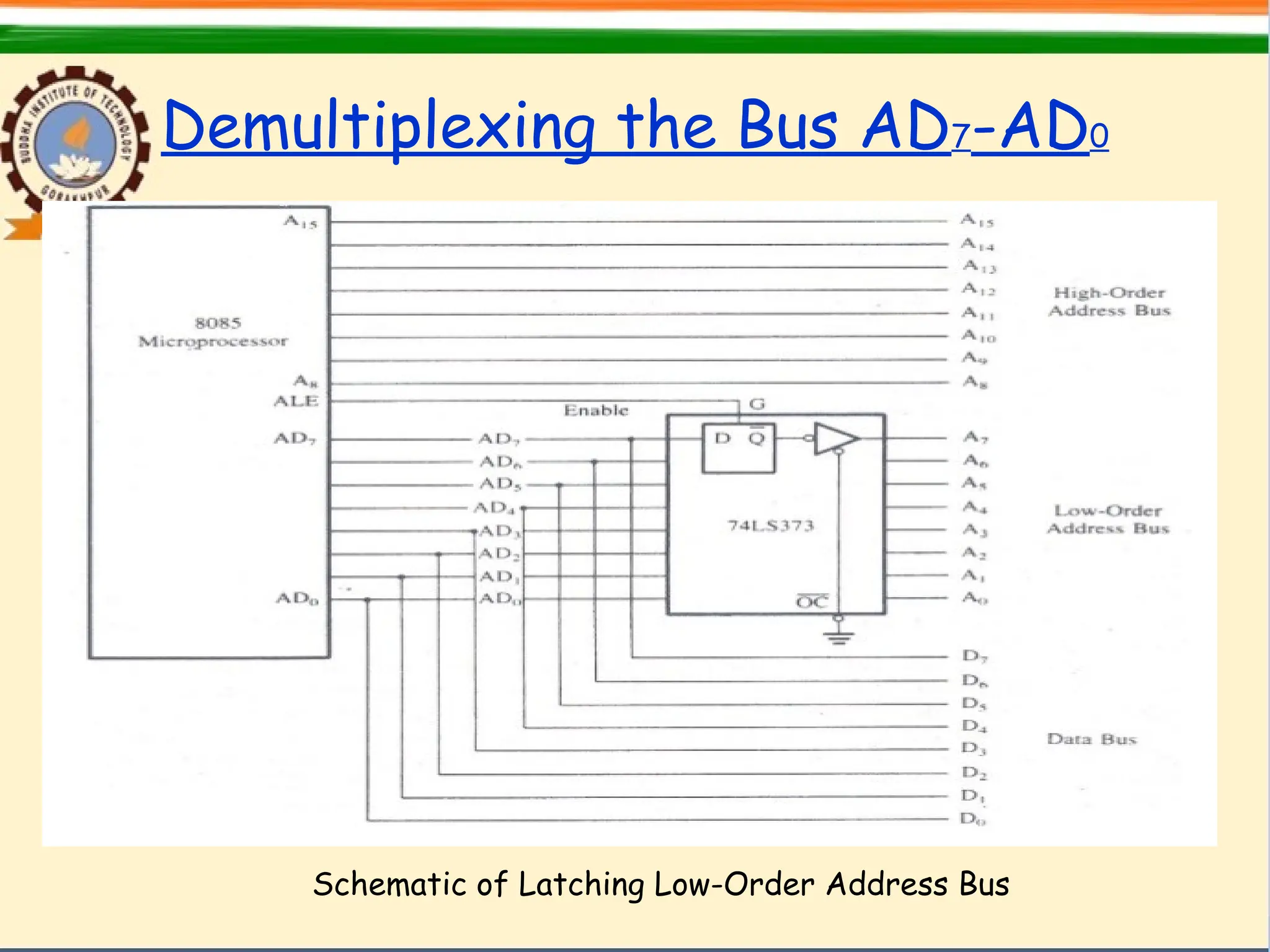
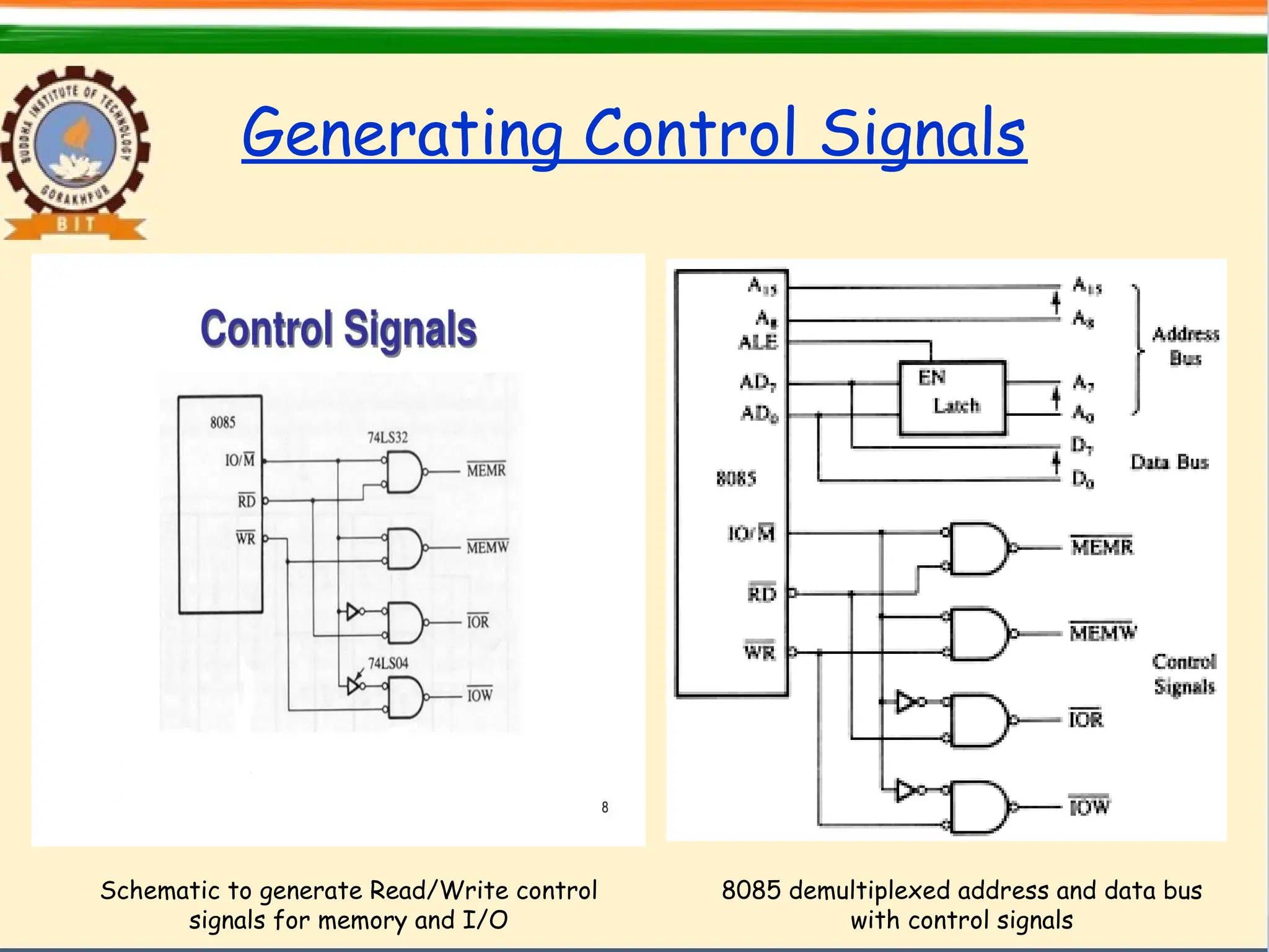
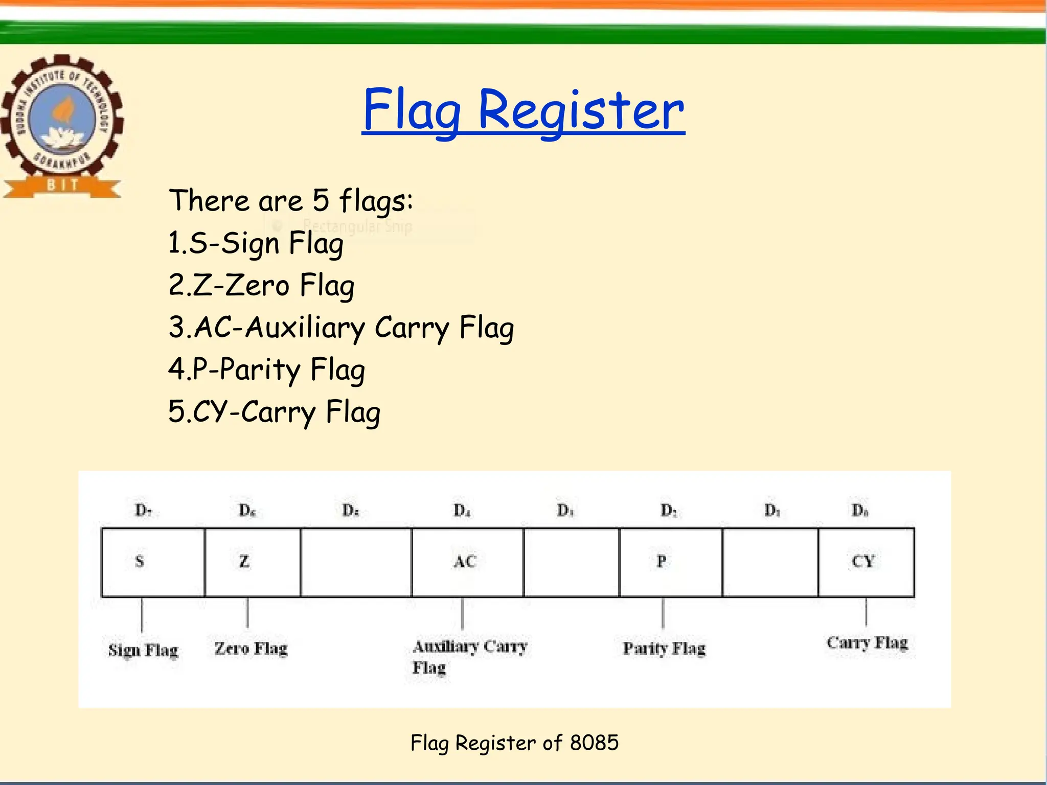
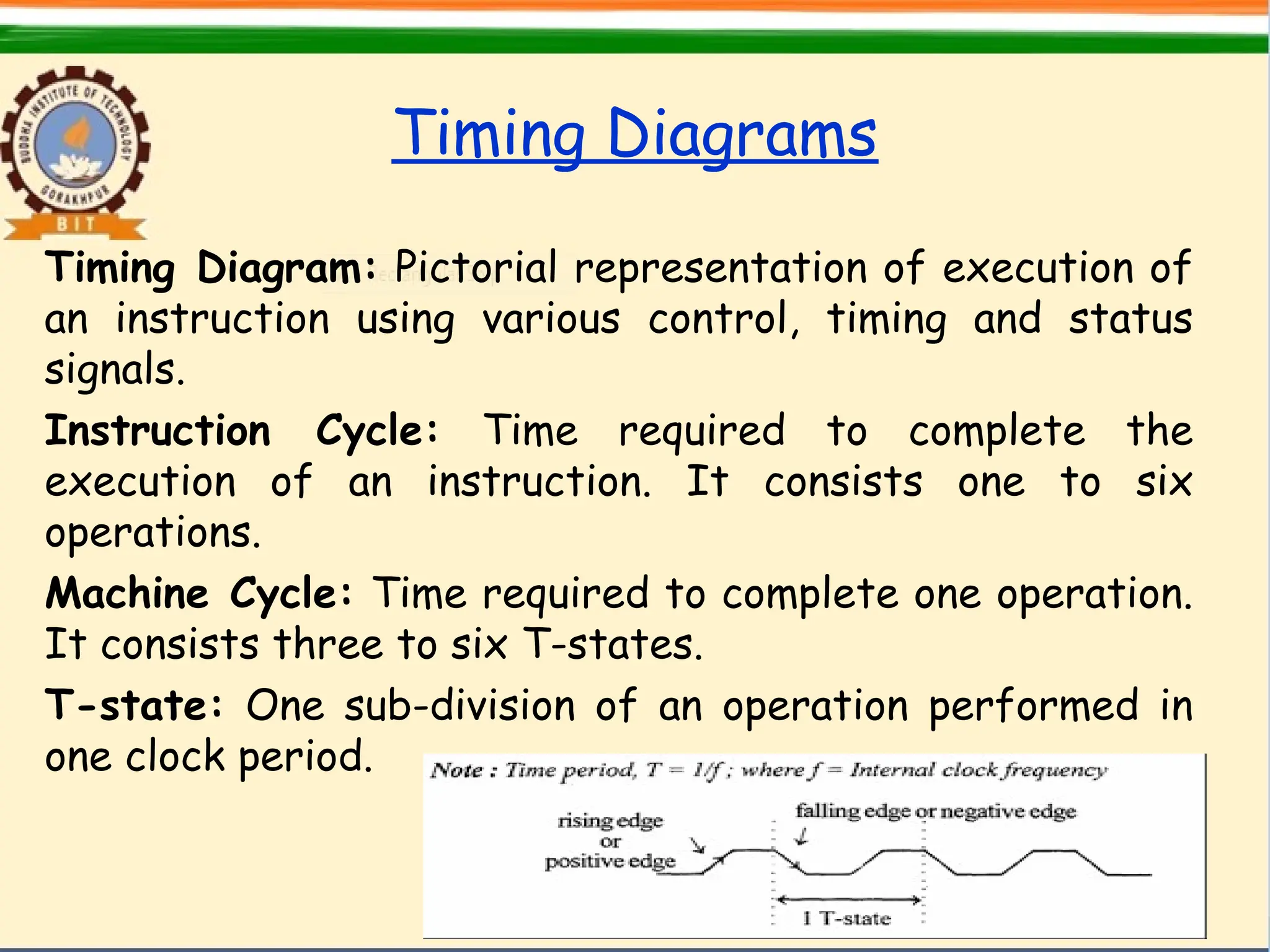
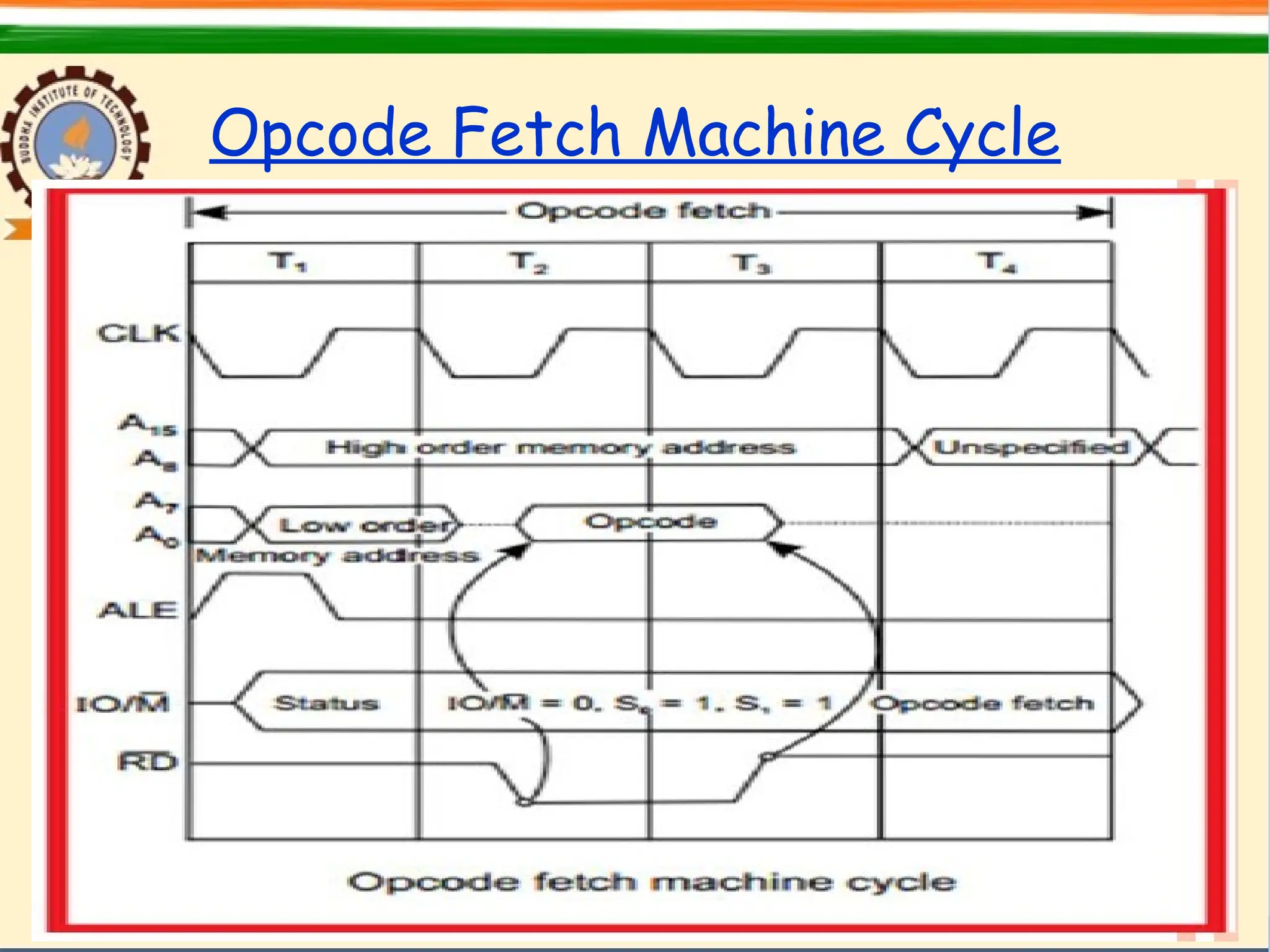
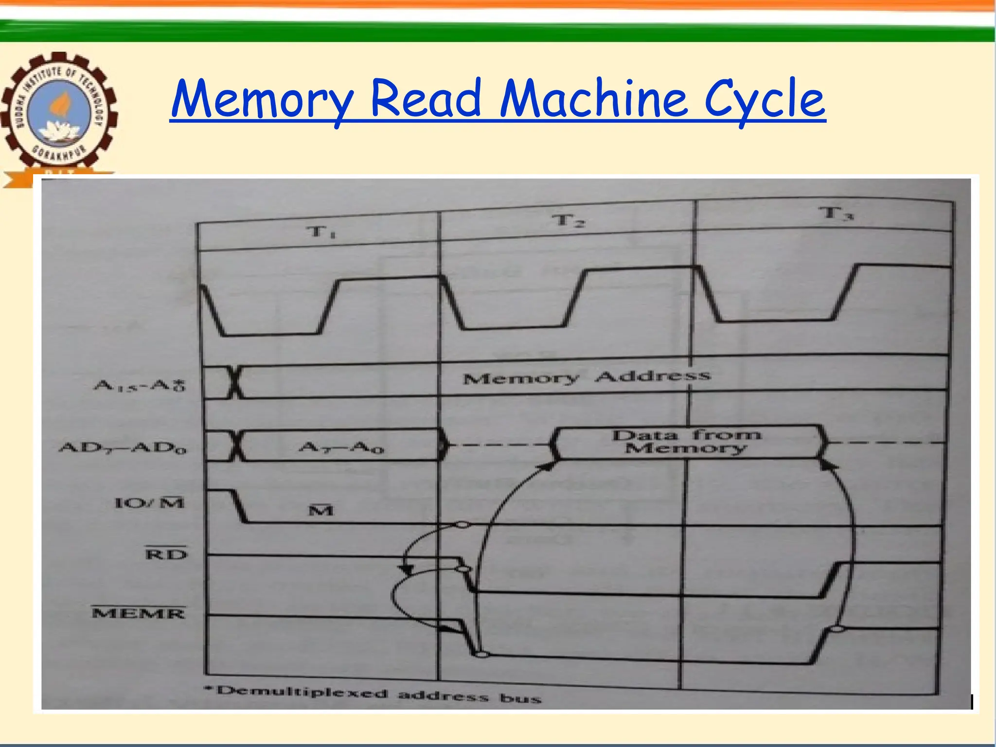
KEMBAR78
PPT Of Unit 1 of Microprocessor & Microcontroller.ppt
MICROPROCESSOR &
MICROCONTROLLER
UNIT 1
INTRODUCTION TO MICROPROCESSOR
Faculty: GHANSHYAM MISHRA
Department Of ECE
Text Books:
1. Microprocessor Architecture, Programming, and
Applications with the 8085 – Ramesh Gaonkar
A Programmable Machine
• Multipurpose,
programmable, clock-
driven, register-based
electronic device.
• Memory-storage device.
• Input- to accept data
• Output- to provide result.
Traditional Block Diagram of a
Computer
•Four components-
1.Memory
2.Input device
3.Output device
4.CPU
Computer with Microprocessor as
CPU
•CPU on a single chip-
microprocessor
Block Diagram of a Microcontroller
Microcontroller- an
entire computer on a
single chip.
Advances in Semiconductor
Technology
• SSI- Small Scale Integration
• MSI-Medium Scale Integration
• LSI- Large Scale Integration
• VLSI- Very Large Scale Integration
Evolution of Microprocessors
First microprocessor released by IntelCorporation in
1971 was INTEL 4004.
First Generation Microprocessors:
• Introduced between 1971 and 1973.
• Designed using PMOS technology.
• Having low cost, slow speed and low output currents.
• Not compatible with TTL.
• 4-bit processors- INTEL 4004, INTEL 4040,
NATIONAL IMP-4.
• 8-bit processors- INTEL 8008, NATIONALIMP-8.
• 16 bit processors- NATIONAL PACE.
Evolution of Microprocessors
Second Generation Microprocessors:
• Introduced in 1973.
• Designed using NMOS technology.
• Offers faster speed and higher density.
• Compatible with TTL.
• 8-bit processors- INTEL 8080, INTEL 8085,
NATIONAL cMP-8.
• 12 bit Processors- TOSHIBA TLCS- 12.
• 16 bit processors- TI TMS 9900.
Evolution of Microprocessors
Third Generation Microprocessors:
• Introduced after 1978.
• Designed using HMOS technology.
• Offers high speed and very strong processing
capability.
• Easier to program.
• 16 bit processors- INTEL 8086, INTEL 8088,
INTEL 80186, INTEL 80286, TI TMS 99000.
Evolution of Microprocessors
Fourth Generation Microprocessors:
• Introduced in 1980.
• Designed using low power version of HMOS
technology called HCMOS.
• 32 bit processors- INTEL 80386, INTEL 80486,
MOTOROLA M68020.
Fifth Generation Microprocessors:
• INTEL pentium released in 1993.
• 32-bit processor.
Microprocessor-based System
with Bus Architecture
• Microprocessor-
ALU
Register Array
Control Unit
• Memory-
ROM
RAM
• I/O
• System Bus
Microprocessor buses and Its
Operations
Three sets of
communication lines are
called buses-
1.Address bus
2.Data bus
3.Control bus
The 8085 Bus Architecture
Address Bus-
•used to identify a peripheral or memory location.
•Consists of 16 address lines: A0 – A15.
•Operates in unidirectional mode: The address bits are always sent
from the MPU to peripheral devices, not reverse.
•16 address lines are capable of addressing a total of 216
= 65,536
(64k) memory locations.
•Address locations: 0000 (hex) – FFFF (hex).
Data Bus-
•Consists of 8 data lines: D0 – D7.
• Operates in bidirectional mode: The data bits are sent from the
MPU to peripheral devices, as well as from the peripheral devices
to the MPU.
• Data range: 00 (hex) – FF (hex)
Control Bus-
• Consists of various lines carrying the control signals such as read /
write enable, flag bits.
Microprocessor Architecture and
Its Operations
Microprocesor functions are classified as-
1. Microprocessor-initiated operations
•Memory read.
•Memory write.
•I/O read.
•I/O write.
2. Internal operatins
•Store 8-bit data.
•Perform arithmetic and logical operations.
•Test for conditions.
•Sequence the execution of instructions.
•Store data temporarily.
3. Peripheral ( or externally initiated ) operations
•Reset
•Interrupt
•Ready
•Hold
Programming Model of 8085
Register Array:
•Six general purpose registers- B,C,D,E,H,L.
Accumulator:
•Used to store 8 bit data and to perform arithmetic and
logical operations.
•Used to store the result.
Program Counter and Stack Pointer:
•Used to hold memory address.
W and Z Registers:
•Not available to the programmer.
•Used to hold 8-bit data during execution of some
instructions.
General features of 8085
Microprocessor for 2 marks
• 8-bit microprocessor introduced by INTEL in 1977.
• Has 16 address lines.
• 40 pin IC present in DIP.
• Capable of addressing 64KB of memory.
• Has 8 data lines.
• Low-order address bus is multiplexed with the data bus.
• Requires a +5V single power supply.
• Can operate with 3MHz clock.
General features of 8085
Microprocessor for 10 marks
• The Intel 8085 is an 8-bit microprocessor that was
widely used in the late 1970s and early 1980s. It
has several general features:
• 8-bit Data Bus: The 8085 has an 8-bit data bus,
which means it can process data in 8-bit chunks at
a time.
• 16-bit Address Bus: It has a 16-bit address bus,
allowing it to address up to 64 KB (64,000 memory
locations) of memory.
• Clock Speed: The 8085 typically operates at a clock
speed of 3 MHz, although some versions and
applications could run at different frequencies.
• Registers: It has six general-purpose registers (B, C, D, E, H,
and L), which can be combined as register pairs (BC, DE, and
HL). It also has a 16-bit stack pointer (SP) and a 16-bit
program counter (PC).
• Instruction Set: The 8085 has a relatively simple and
straightforward instruction set with 74 instructions.
Instructions are typically one to three bytes long.
• Flags: It has five flags in the flag register: Sign (S), Zero (Z),
Auxiliary Carry (AC), Parity (P), and Carry (CY). These flags are
used to indicate various conditions after arithmetic and logic
operations.
• Interrupts: The 8085 supports five interrupt lines: TRAP,
RST 7.5, RST 6.5, RST 5.5, and INTR. It can handle both
hardware and software interrupts
• serial I/O Control: It has serial input and output lines
that can be controlled for serial data communication.
• Instruction Pipelining: The 8085 uses a simple
pipeline architecture, which means it can fetch the
next instruction while executing the current one.
• Memory Addressing Modes: It supports various
addressing modes, including direct addressing,
register addressing, immediate addressing, and
indirect addressing.
• On-Chip Clock Generator: The 8085 includes an on-
chip clock generator circuit, simplifying the external
circuitry required for clock generation.
Power Supply: It typically operates on a single +5V power
supply.
Minimum and Maximum Mode: The 8085 can operate in
minimum mode, where it uses externally connected
components for interfacing, or maximum mode, where it
uses additional pins to communicate with external
components like co-processors.
Instruction Execution Time: The execution time for most
instructions ranges from 4 to 10 machine cycles,
depending on the complexity of the instruction.
Binary Coded Decimal (BCD) Arithmetic: The 8085 has
instructions to perform BCD arithmetic operations directly
Pin Description of 8085
The signals of 8085 can be classified into 6 groups-
1.Address bus
2.Data bus
3.Control and status signals
4.Power supply and frequency signals
5.Externally initiated signals
6.Serial I/O ports
• A15-A8 (Address Bus): These are the high-order address
lines used to specify the memory or I/O device address. The
8085 can address up to 64K (64,000) different memory
locations.
• AD7-AD0 (Data Bus): These are the bi-directional data lines
used to transfer data between the microprocessor and
memory or I/O devices. The 8085 is an 8-bit
microprocessor, so it can transfer 8 bits of data at a time.
• ALE (Address Latch Enable): ALE is used to latch the
address from the multiplexed address/data bus into the
external latch or memory ICs. It is activated during the
first clock cycle of each machine cycle.
• S0 and S1 (Status Lines): These status lines indicate the
status of the microprocessor during different machine
cycles. They are used for interfacing with other devices and
for control purposes.
• SID (Serial Input Data): This pin is used for serial data
input when interfacing with serial devices.
• SOD (Serial Output Data): This pin is used for serial data
output when interfacing with serial devices.
• RESET IN (Reset Input): When a high signal is applied to
this pin, it resets the microprocessor, causing it to restart
execution from the address 0000H.
• X1 and X2 (Crystal Oscillator Input and Output): These pins
are used to connect an external crystal oscillator or clock
source to provide the microprocessor with the required clock
signal for operation.
• INTR (Interrupt Request): This is the interrupt request
input. When a high-level signal is applied to this pin, it
requests the microprocessor to service an interrupt.
• INTA (Interrupt Acknowledge): This output is used to
acknowledge an interrupt request. It indicates that the
microprocessor is ready to service an interrupt.
• HOLD and HLDA (Hold Request and Hold Acknowledge):
These pins are used for holding the microprocessor's
operation temporarily, allowing external devices to gain
control of the system bus.
• READY: This input indicates to the microprocessor that the
external devices are ready to provide or accept data. It is
used to insert wait states if needed.
• RST 7.5, RST 6.5, and RST 5.5: These are hardware
interrupt request inputs for specific vectored interrupts.
• TRAP: This is a non-maskable interrupt (NMI) input. When a
high-level signal is applied to this pin, it generates an NMI.
• RESET OUT: This is the reset output pin. It provides a
reset signal to other devices in the system when the
microprocessor is reset.
• +5V and GND: These pins are used to provide the power
supply to the microprocessor. +5V is the positive voltage
supply, and GND is the ground reference.
The remaining pins are used for various control
signals, clock-related signals, and interfacing with
memory and peripheral devices.
Understanding the pin diagram of the 8085
microprocessor is essential for interfacing it with
memory, input/output devices, and other components
in a computer or embedded system design.
Memory
• Stores binary instructions and data for the microprocessor.
• Can be classified in two groups- Prime (main) memory and storage memory.
• Prime memory- Read/Write memory (R/WM) and Read-Only memory (ROM).
• R/WM-
Made of registers and each register has a group of flip-flops.
Flip-flop- memory cell.
Memory word- number of bits stored in a register.
Used to hold programs and store data.
• ROM-
Stores information permanently in the form of diodes.
Group of diodes- register.
• Memory Address- binary numbers by which all registers are identified.
• To communicate with memory, the MPU should be able to-
select the chip.
identify the register, and
read from or write into the register.
Memory Model
R/W Memory Model and ROM Model
Memory Map and Addresses
Memory and Instruction Fetch
Memory Classification
R/WM-
•Popularly known as RAM.
•Information stored can be altered.
•Volatile.
•Two types- Static and Dynamic.
Static Memory (SRAM)-
•Made up of flip flops, stores the bit as a voltage.
•Low density but high speed.
•More expensive and consumes more power.
Dynamic Memory (DRAM)-
•Made up of MOS transistor gates, stores the bit as a charge.
•High density and low power consumption.
•Cheaper.
• Refreshing is required.
ROM-
• Nonvolatile memory.
• Information can be read only.
• Permanent group includes- masked ROM and PROM.
• Semipermanent group includes- EPROM and EE-PROM.
Masked ROM-
• Bit pattern is permanently recorded.
PROM-
• Programmable Read-Only Memory.
• Memory can be programmed by the user.
• Information stored is permanent.
EPROM-
•Erasable Programmable Read-Only Memory.
•Erasing is done through ultraviolet light.
EEPROM-
•Electrically Erasable PROM.
•Erasing is done using electrical signals.
Flash Memory-
•Can be erased either in it entirely or at the sector or block level.
Input and Output Devices
There are two different methods by which I/O devices can be
identified-
1.I/Os with 8 bit addresses ( Peripheral –mapped I/O)-
• MPU uses eight address lines to identify an I/O device.
• Also known as I/O mapped I/O.
• The I/O map is independent of the memory map; 256 input
device and 256. output device can be connected.
• Less hardware is required to decode 8-bit address.
• I/O devices are differentiated by the control signals.
• The I/O devices are treated as I/O devices and the memory is
treated as memory.
2. I/Os with 16 bit addresses ( Memory–mapped I/O)-
• MPU uses 16 address line.
• The processor treats the I/O devices like any other memory
location
• MPU uses the same control signal and instructions as those of
memory.
• I/Os and memory share the same memory map (64K).
Demultiplexing the Bus AD7-AD0
Schematic of Latching Low-Order Address Bus
• ALE is high every time the 8085 begins an
operation.
• When the ALE is high, the latch is transparent.
• When the ALE is low, data byte is latched until
the next ALE, and hence output of the latch
represents the low-order address.
Generating Control Signals
Schematic to generate Read/Write control
signals for memory and I/O
8085 demultiplexed address and data bus
with control signals
Flag Register
There are 5 flags:
1.S-Sign Flag
2.Z-Zero Flag
3.AC-Auxiliary Carry Flag
4.P-Parity Flag
5.CY-Carry Flag
Flag Register of 8085
Timing Diagrams
Timing Diagram: Pictorial representation of execution of
an instruction using various control, timing and status
signals.
Instruction Cycle: Time required to complete the
execution of an instruction. It consists one to six
operations.
Machine Cycle: Time required to complete one operation.
It consists three to six T-states.
T-state: One sub-division of an operation performed in
one clock period.
Opcode Fetch Machine Cycle
• It is the first step of executing any instruction.
• Microprocessor brings in the instruction’s opcode from
memory.
• The control and status signals are set as follows:
• IO/M=0, S0 and S1 both are 1.
• This machine cycle has 4 or 6 T-states. First three T-
states are used to fetch the opcode and T4 is used to
decode and execute.
Opcode Fetch Machine Cycle
Memory Read Machine Cycle
8085 Timing for Execution of the
Instruction MVI A,32H

PPT Of Unit 1 of Microprocessor & Microcontroller.ppt

  • 1.
    MICROPROCESSOR & MICROCONTROLLER UNIT 1 INTRODUCTIONTO MICROPROCESSOR Faculty: GHANSHYAM MISHRA Department Of ECE
  • 2.
    Text Books: 1. MicroprocessorArchitecture, Programming, and Applications with the 8085 – Ramesh Gaonkar
  • 3.
    A Programmable Machine •Multipurpose, programmable, clock- driven, register-based electronic device. • Memory-storage device. • Input- to accept data • Output- to provide result.
  • 4.
    Traditional Block Diagramof a Computer •Four components- 1.Memory 2.Input device 3.Output device 4.CPU
  • 5.
    Computer with Microprocessoras CPU •CPU on a single chip- microprocessor
  • 6.
    Block Diagram ofa Microcontroller Microcontroller- an entire computer on a single chip.
  • 7.
    Advances in Semiconductor Technology •SSI- Small Scale Integration • MSI-Medium Scale Integration • LSI- Large Scale Integration • VLSI- Very Large Scale Integration
  • 8.
    Evolution of Microprocessors Firstmicroprocessor released by IntelCorporation in 1971 was INTEL 4004. First Generation Microprocessors: • Introduced between 1971 and 1973. • Designed using PMOS technology. • Having low cost, slow speed and low output currents. • Not compatible with TTL. • 4-bit processors- INTEL 4004, INTEL 4040, NATIONAL IMP-4. • 8-bit processors- INTEL 8008, NATIONALIMP-8. • 16 bit processors- NATIONAL PACE.
  • 9.
    Evolution of Microprocessors SecondGeneration Microprocessors: • Introduced in 1973. • Designed using NMOS technology. • Offers faster speed and higher density. • Compatible with TTL. • 8-bit processors- INTEL 8080, INTEL 8085, NATIONAL cMP-8. • 12 bit Processors- TOSHIBA TLCS- 12. • 16 bit processors- TI TMS 9900.
  • 10.
    Evolution of Microprocessors ThirdGeneration Microprocessors: • Introduced after 1978. • Designed using HMOS technology. • Offers high speed and very strong processing capability. • Easier to program. • 16 bit processors- INTEL 8086, INTEL 8088, INTEL 80186, INTEL 80286, TI TMS 99000.
  • 11.
    Evolution of Microprocessors FourthGeneration Microprocessors: • Introduced in 1980. • Designed using low power version of HMOS technology called HCMOS. • 32 bit processors- INTEL 80386, INTEL 80486, MOTOROLA M68020. Fifth Generation Microprocessors: • INTEL pentium released in 1993. • 32-bit processor.
  • 12.
    Microprocessor-based System with BusArchitecture • Microprocessor- ALU Register Array Control Unit • Memory- ROM RAM • I/O • System Bus
  • 13.
    Microprocessor buses andIts Operations Three sets of communication lines are called buses- 1.Address bus 2.Data bus 3.Control bus The 8085 Bus Architecture
  • 14.
    Address Bus- •used toidentify a peripheral or memory location. •Consists of 16 address lines: A0 – A15. •Operates in unidirectional mode: The address bits are always sent from the MPU to peripheral devices, not reverse. •16 address lines are capable of addressing a total of 216 = 65,536 (64k) memory locations. •Address locations: 0000 (hex) – FFFF (hex). Data Bus- •Consists of 8 data lines: D0 – D7.
  • 15.
    • Operates inbidirectional mode: The data bits are sent from the MPU to peripheral devices, as well as from the peripheral devices to the MPU. • Data range: 00 (hex) – FF (hex) Control Bus- • Consists of various lines carrying the control signals such as read / write enable, flag bits.
  • 16.
    Microprocessor Architecture and ItsOperations Microprocesor functions are classified as- 1. Microprocessor-initiated operations •Memory read. •Memory write. •I/O read. •I/O write. 2. Internal operatins •Store 8-bit data. •Perform arithmetic and logical operations. •Test for conditions. •Sequence the execution of instructions. •Store data temporarily. 3. Peripheral ( or externally initiated ) operations •Reset •Interrupt •Ready •Hold
  • 18.
  • 19.
    Register Array: •Six generalpurpose registers- B,C,D,E,H,L. Accumulator: •Used to store 8 bit data and to perform arithmetic and logical operations. •Used to store the result. Program Counter and Stack Pointer: •Used to hold memory address. W and Z Registers: •Not available to the programmer. •Used to hold 8-bit data during execution of some instructions.
  • 20.
    General features of8085 Microprocessor for 2 marks • 8-bit microprocessor introduced by INTEL in 1977. • Has 16 address lines. • 40 pin IC present in DIP. • Capable of addressing 64KB of memory. • Has 8 data lines. • Low-order address bus is multiplexed with the data bus. • Requires a +5V single power supply. • Can operate with 3MHz clock.
  • 21.
    General features of8085 Microprocessor for 10 marks • The Intel 8085 is an 8-bit microprocessor that was widely used in the late 1970s and early 1980s. It has several general features: • 8-bit Data Bus: The 8085 has an 8-bit data bus, which means it can process data in 8-bit chunks at a time. • 16-bit Address Bus: It has a 16-bit address bus, allowing it to address up to 64 KB (64,000 memory locations) of memory. • Clock Speed: The 8085 typically operates at a clock speed of 3 MHz, although some versions and applications could run at different frequencies.
  • 22.
    • Registers: Ithas six general-purpose registers (B, C, D, E, H, and L), which can be combined as register pairs (BC, DE, and HL). It also has a 16-bit stack pointer (SP) and a 16-bit program counter (PC). • Instruction Set: The 8085 has a relatively simple and straightforward instruction set with 74 instructions. Instructions are typically one to three bytes long. • Flags: It has five flags in the flag register: Sign (S), Zero (Z), Auxiliary Carry (AC), Parity (P), and Carry (CY). These flags are used to indicate various conditions after arithmetic and logic operations. • Interrupts: The 8085 supports five interrupt lines: TRAP, RST 7.5, RST 6.5, RST 5.5, and INTR. It can handle both hardware and software interrupts
  • 23.
    • serial I/OControl: It has serial input and output lines that can be controlled for serial data communication. • Instruction Pipelining: The 8085 uses a simple pipeline architecture, which means it can fetch the next instruction while executing the current one. • Memory Addressing Modes: It supports various addressing modes, including direct addressing, register addressing, immediate addressing, and indirect addressing. • On-Chip Clock Generator: The 8085 includes an on- chip clock generator circuit, simplifying the external circuitry required for clock generation.
  • 24.
    Power Supply: Ittypically operates on a single +5V power supply. Minimum and Maximum Mode: The 8085 can operate in minimum mode, where it uses externally connected components for interfacing, or maximum mode, where it uses additional pins to communicate with external components like co-processors. Instruction Execution Time: The execution time for most instructions ranges from 4 to 10 machine cycles, depending on the complexity of the instruction. Binary Coded Decimal (BCD) Arithmetic: The 8085 has instructions to perform BCD arithmetic operations directly
  • 25.
  • 26.
    The signals of8085 can be classified into 6 groups- 1.Address bus 2.Data bus 3.Control and status signals 4.Power supply and frequency signals 5.Externally initiated signals 6.Serial I/O ports
  • 27.
    • A15-A8 (AddressBus): These are the high-order address lines used to specify the memory or I/O device address. The 8085 can address up to 64K (64,000) different memory locations. • AD7-AD0 (Data Bus): These are the bi-directional data lines used to transfer data between the microprocessor and memory or I/O devices. The 8085 is an 8-bit microprocessor, so it can transfer 8 bits of data at a time. • ALE (Address Latch Enable): ALE is used to latch the address from the multiplexed address/data bus into the external latch or memory ICs. It is activated during the first clock cycle of each machine cycle.
  • 28.
    • S0 andS1 (Status Lines): These status lines indicate the status of the microprocessor during different machine cycles. They are used for interfacing with other devices and for control purposes. • SID (Serial Input Data): This pin is used for serial data input when interfacing with serial devices. • SOD (Serial Output Data): This pin is used for serial data output when interfacing with serial devices. • RESET IN (Reset Input): When a high signal is applied to this pin, it resets the microprocessor, causing it to restart execution from the address 0000H.
  • 29.
    • X1 andX2 (Crystal Oscillator Input and Output): These pins are used to connect an external crystal oscillator or clock source to provide the microprocessor with the required clock signal for operation. • INTR (Interrupt Request): This is the interrupt request input. When a high-level signal is applied to this pin, it requests the microprocessor to service an interrupt. • INTA (Interrupt Acknowledge): This output is used to acknowledge an interrupt request. It indicates that the microprocessor is ready to service an interrupt. • HOLD and HLDA (Hold Request and Hold Acknowledge): These pins are used for holding the microprocessor's operation temporarily, allowing external devices to gain control of the system bus.
  • 30.
    • READY: Thisinput indicates to the microprocessor that the external devices are ready to provide or accept data. It is used to insert wait states if needed. • RST 7.5, RST 6.5, and RST 5.5: These are hardware interrupt request inputs for specific vectored interrupts. • TRAP: This is a non-maskable interrupt (NMI) input. When a high-level signal is applied to this pin, it generates an NMI. • RESET OUT: This is the reset output pin. It provides a reset signal to other devices in the system when the microprocessor is reset. • +5V and GND: These pins are used to provide the power supply to the microprocessor. +5V is the positive voltage supply, and GND is the ground reference.
  • 31.
    The remaining pinsare used for various control signals, clock-related signals, and interfacing with memory and peripheral devices. Understanding the pin diagram of the 8085 microprocessor is essential for interfacing it with memory, input/output devices, and other components in a computer or embedded system design.
  • 32.
    Memory • Stores binaryinstructions and data for the microprocessor. • Can be classified in two groups- Prime (main) memory and storage memory. • Prime memory- Read/Write memory (R/WM) and Read-Only memory (ROM). • R/WM- Made of registers and each register has a group of flip-flops. Flip-flop- memory cell. Memory word- number of bits stored in a register. Used to hold programs and store data. • ROM- Stores information permanently in the form of diodes. Group of diodes- register. • Memory Address- binary numbers by which all registers are identified. • To communicate with memory, the MPU should be able to- select the chip. identify the register, and read from or write into the register.
  • 33.
    Memory Model R/W MemoryModel and ROM Model
  • 34.
    Memory Map andAddresses
  • 36.
  • 37.
  • 38.
    R/WM- •Popularly known asRAM. •Information stored can be altered. •Volatile. •Two types- Static and Dynamic. Static Memory (SRAM)- •Made up of flip flops, stores the bit as a voltage. •Low density but high speed. •More expensive and consumes more power. Dynamic Memory (DRAM)- •Made up of MOS transistor gates, stores the bit as a charge. •High density and low power consumption. •Cheaper.
  • 39.
    • Refreshing isrequired. ROM- • Nonvolatile memory. • Information can be read only. • Permanent group includes- masked ROM and PROM. • Semipermanent group includes- EPROM and EE-PROM. Masked ROM- • Bit pattern is permanently recorded. PROM- • Programmable Read-Only Memory. • Memory can be programmed by the user. • Information stored is permanent.
  • 40.
    EPROM- •Erasable Programmable Read-OnlyMemory. •Erasing is done through ultraviolet light. EEPROM- •Electrically Erasable PROM. •Erasing is done using electrical signals. Flash Memory- •Can be erased either in it entirely or at the sector or block level.
  • 41.
    Input and OutputDevices There are two different methods by which I/O devices can be identified- 1.I/Os with 8 bit addresses ( Peripheral –mapped I/O)- • MPU uses eight address lines to identify an I/O device. • Also known as I/O mapped I/O. • The I/O map is independent of the memory map; 256 input device and 256. output device can be connected. • Less hardware is required to decode 8-bit address. • I/O devices are differentiated by the control signals. • The I/O devices are treated as I/O devices and the memory is treated as memory.
  • 42.
    2. I/Os with16 bit addresses ( Memory–mapped I/O)- • MPU uses 16 address line. • The processor treats the I/O devices like any other memory location • MPU uses the same control signal and instructions as those of memory. • I/Os and memory share the same memory map (64K).
  • 43.
    Demultiplexing the BusAD7-AD0 Schematic of Latching Low-Order Address Bus
  • 44.
    • ALE ishigh every time the 8085 begins an operation. • When the ALE is high, the latch is transparent. • When the ALE is low, data byte is latched until the next ALE, and hence output of the latch represents the low-order address.
  • 45.
    Generating Control Signals Schematicto generate Read/Write control signals for memory and I/O 8085 demultiplexed address and data bus with control signals
  • 46.
    Flag Register There are5 flags: 1.S-Sign Flag 2.Z-Zero Flag 3.AC-Auxiliary Carry Flag 4.P-Parity Flag 5.CY-Carry Flag Flag Register of 8085
  • 47.
    Timing Diagrams Timing Diagram:Pictorial representation of execution of an instruction using various control, timing and status signals. Instruction Cycle: Time required to complete the execution of an instruction. It consists one to six operations. Machine Cycle: Time required to complete one operation. It consists three to six T-states. T-state: One sub-division of an operation performed in one clock period.
  • 48.
    Opcode Fetch MachineCycle • It is the first step of executing any instruction. • Microprocessor brings in the instruction’s opcode from memory. • The control and status signals are set as follows: • IO/M=0, S0 and S1 both are 1. • This machine cycle has 4 or 6 T-states. First three T- states are used to fetch the opcode and T4 is used to decode and execute.
  • 49.
  • 50.
  • 51.
    8085 Timing forExecution of the Instruction MVI A,32H