Downloaded 116 times


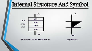
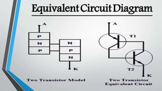

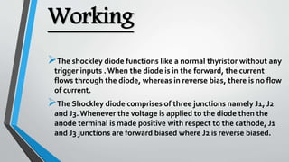
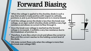
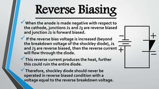


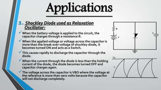
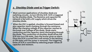


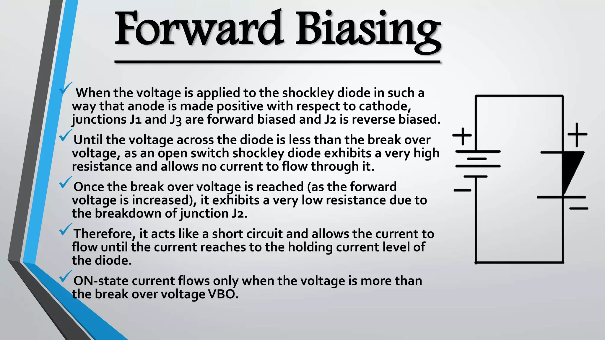
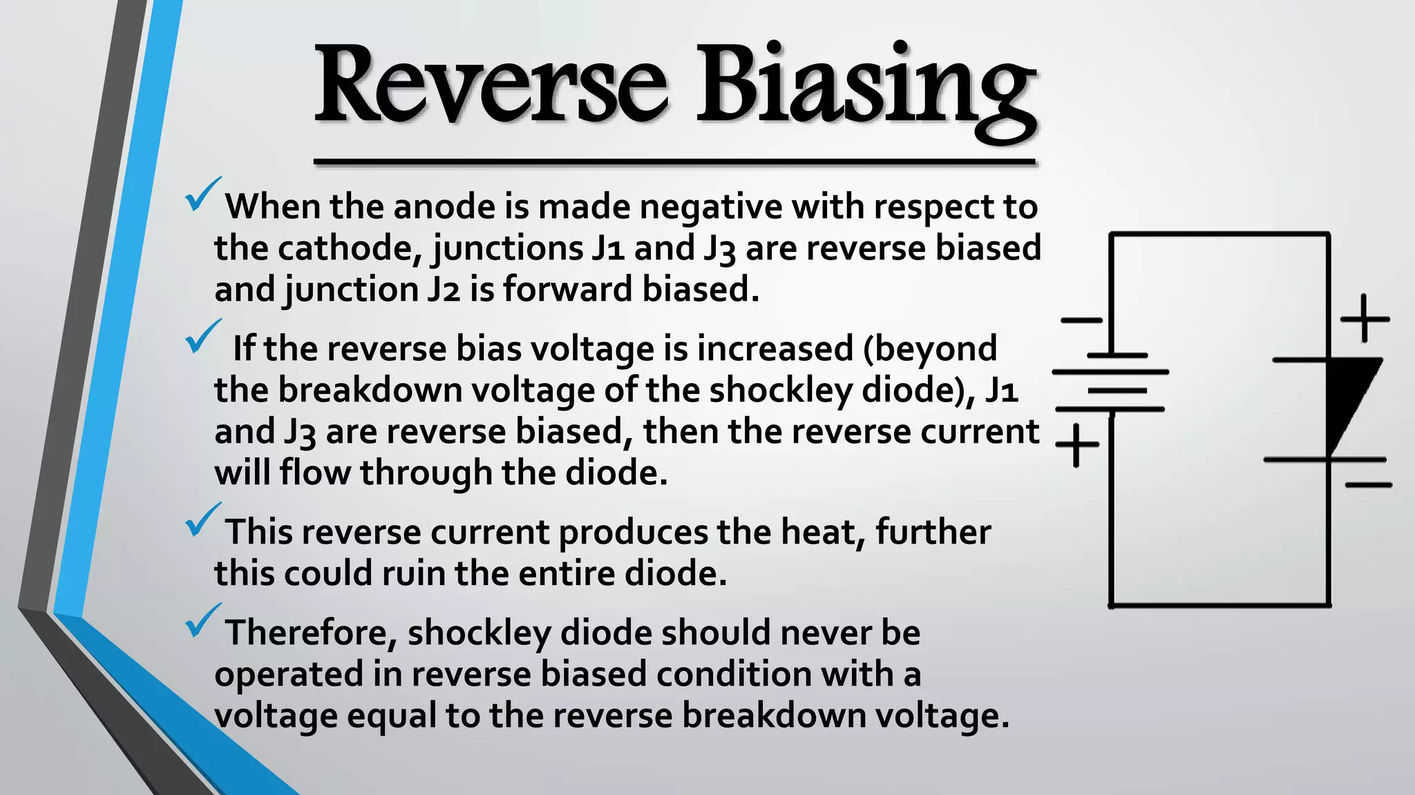


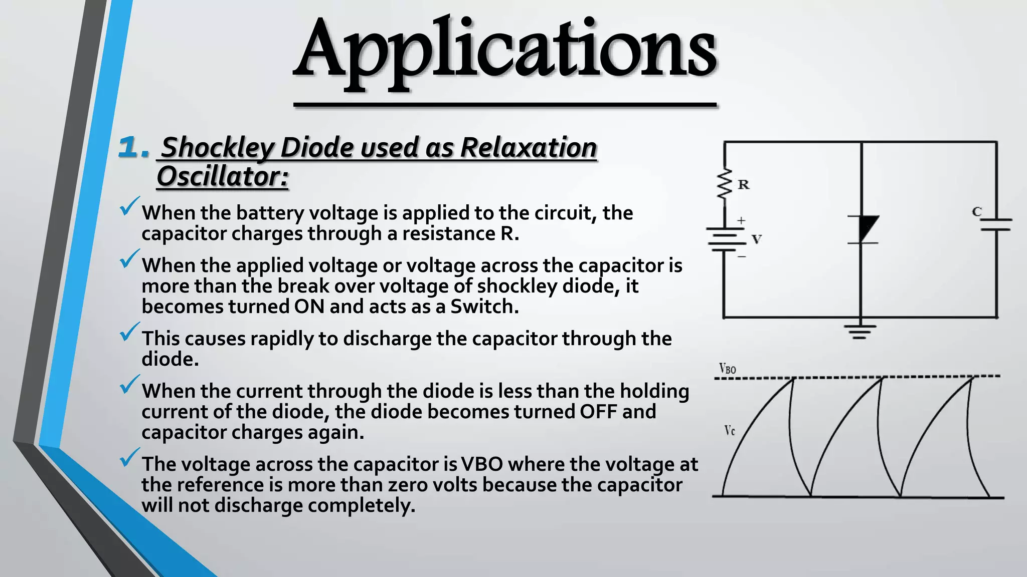
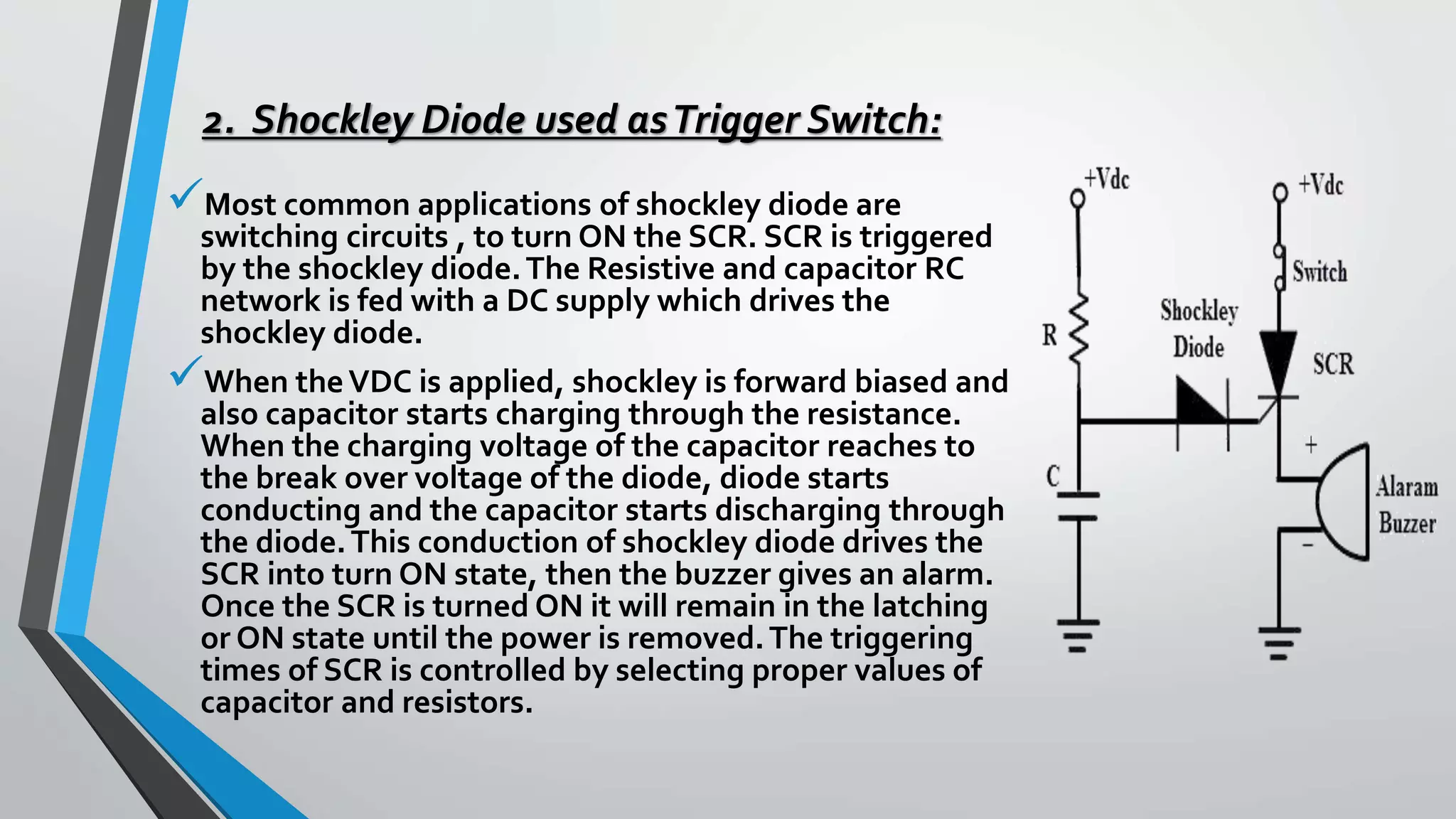


The Shockley diode is a four-layer semiconductor device invented by William Shockley. It consists of three PN junctions (J1, J2, J3) constructed by connecting two transistors. In the forward bias state, J1 and J3 are forward biased while J2 is reverse biased, allowing current to flow. In reverse bias, J1 and J3 are reverse biased while J2 is forward biased, blocking current flow. The diode acts as a closed switch when conducting but turns off when current drops below the holding level. Key applications include use as a relaxation oscillator and triggering SCR devices.


