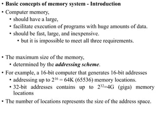
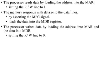
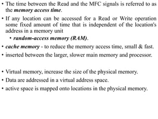
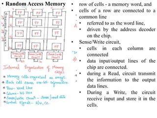
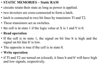
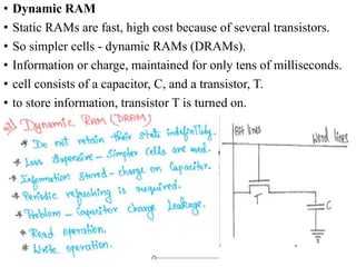
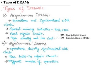
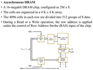
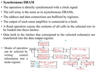
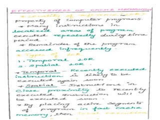
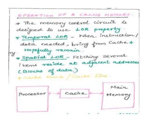
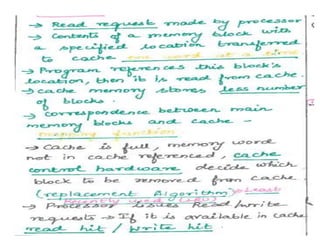
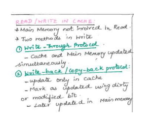
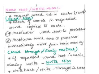
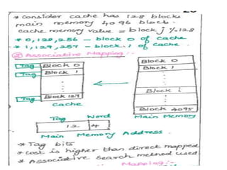
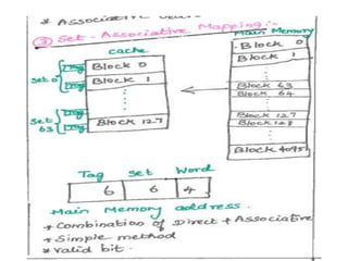
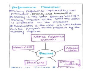
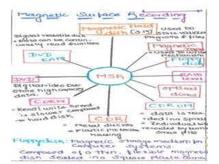
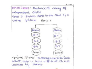
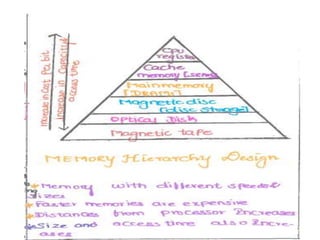
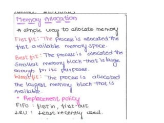
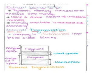
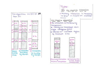
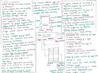
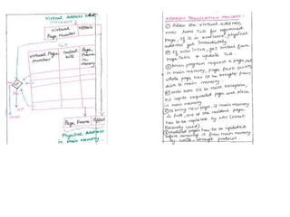
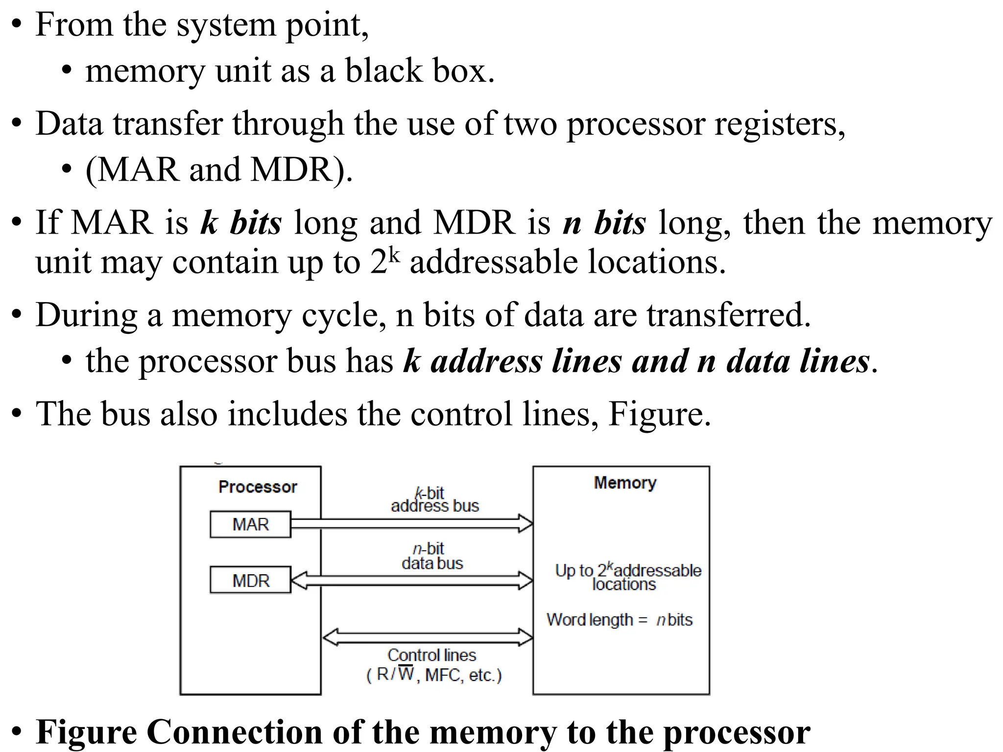
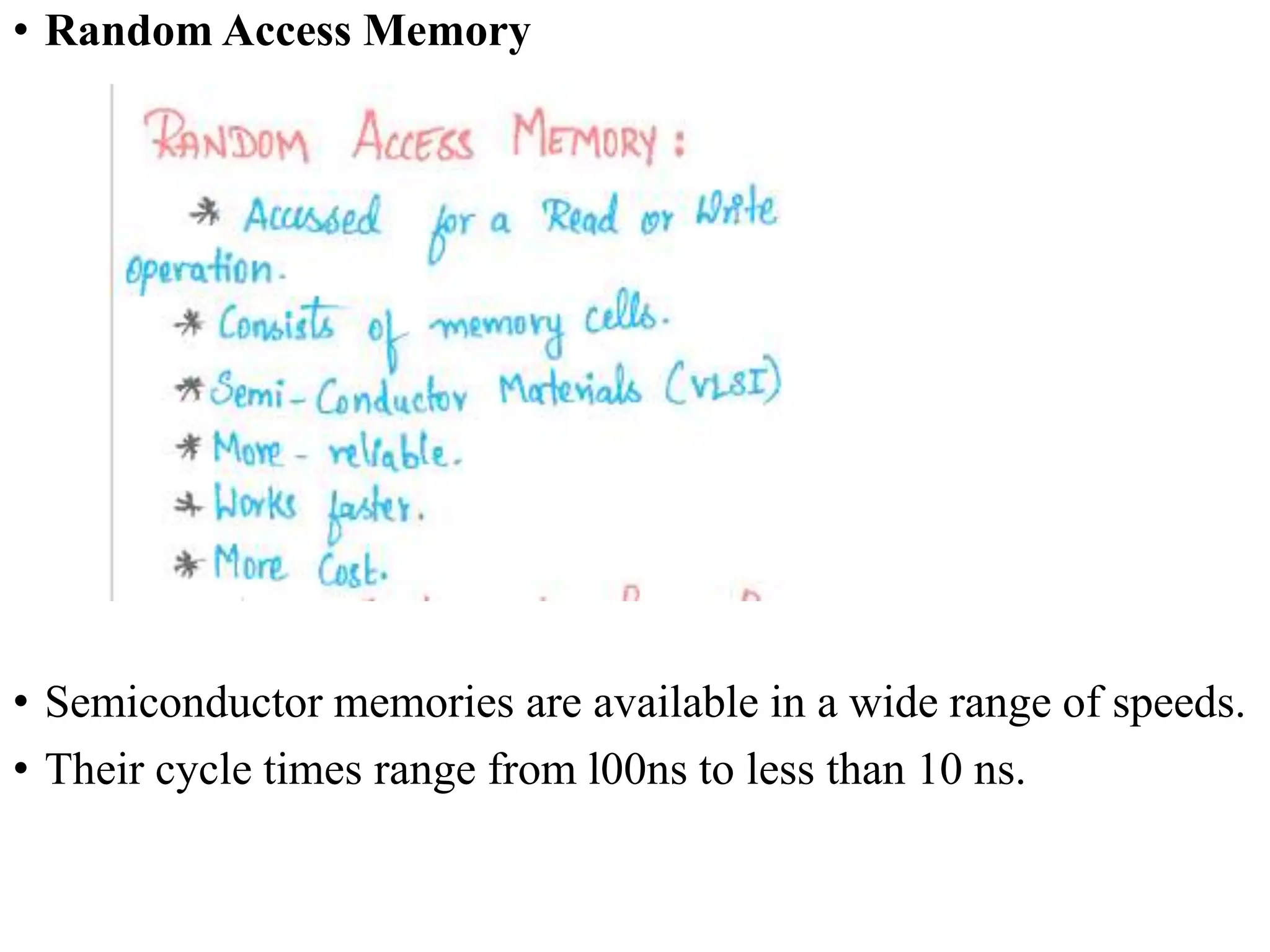
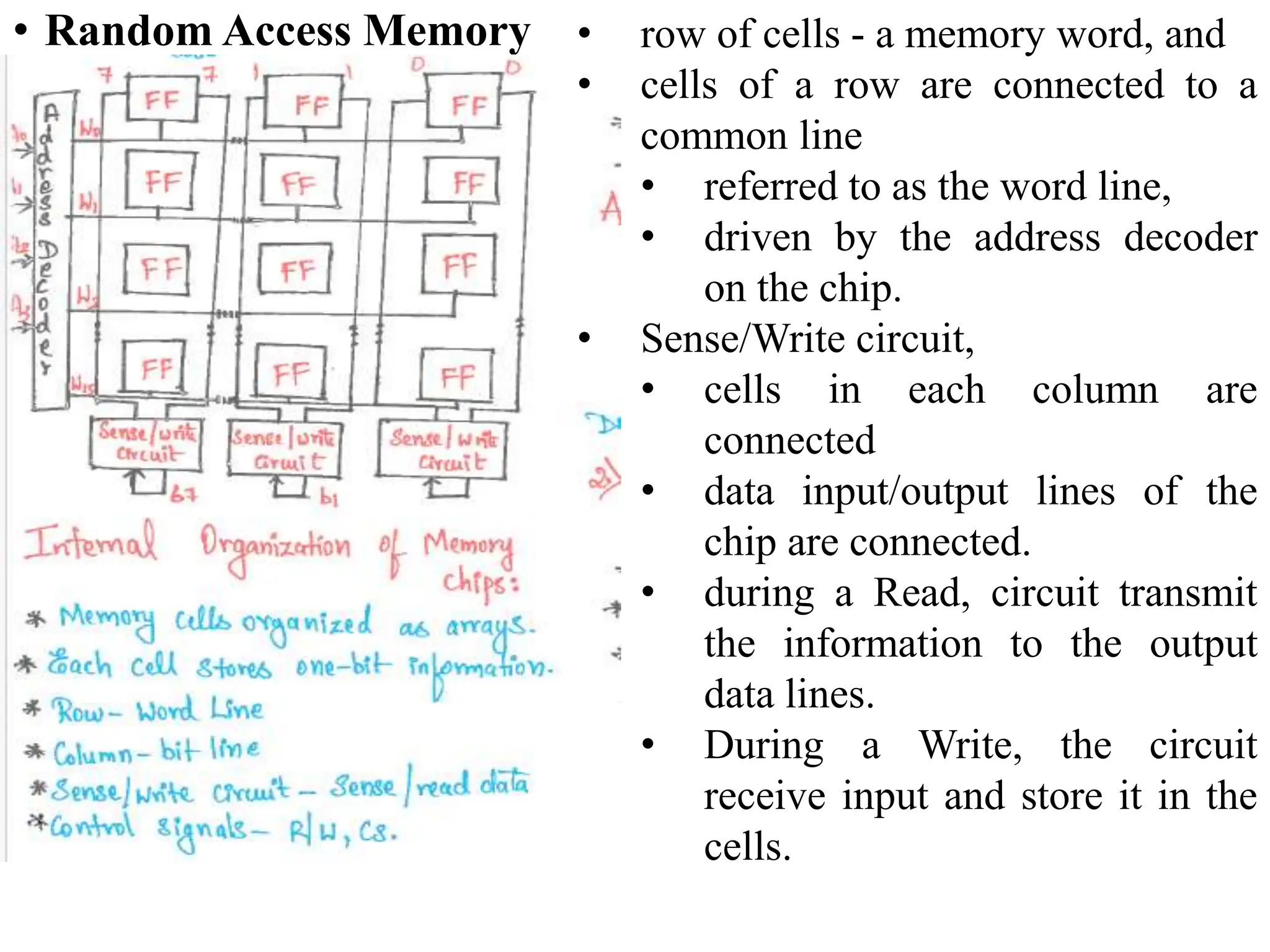
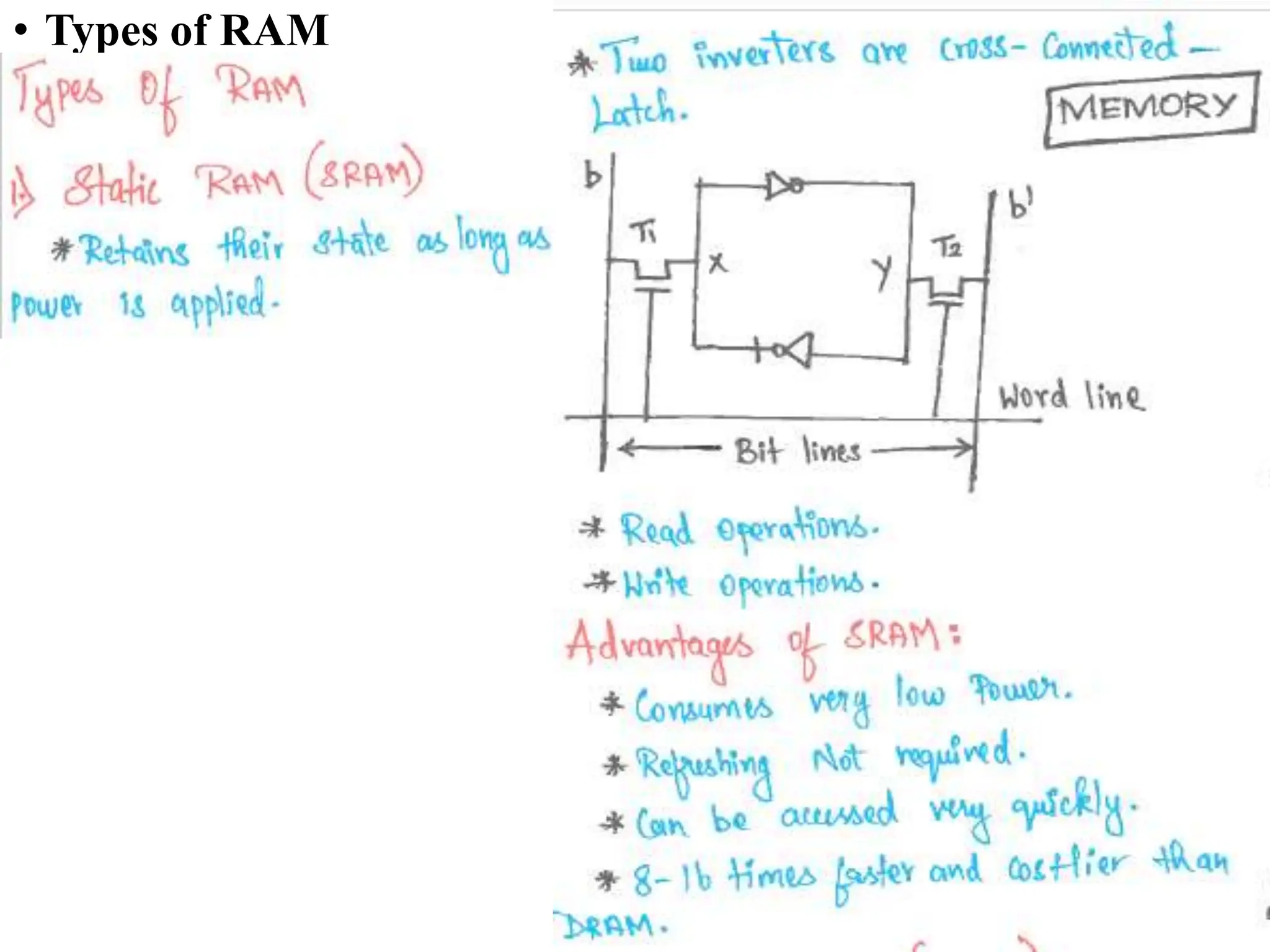
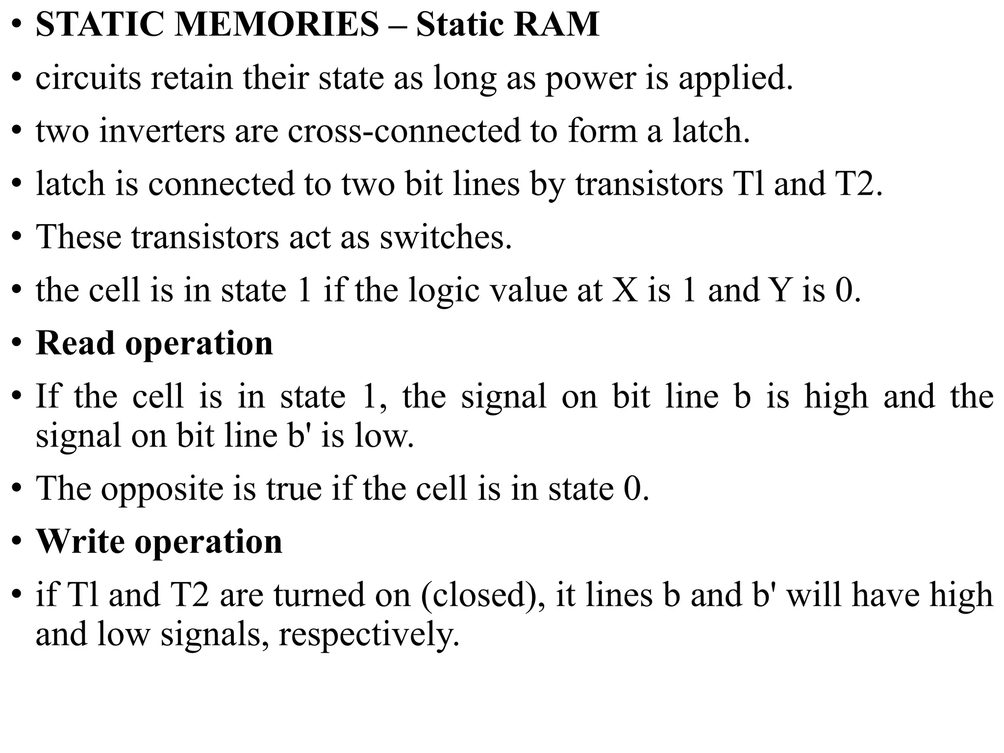
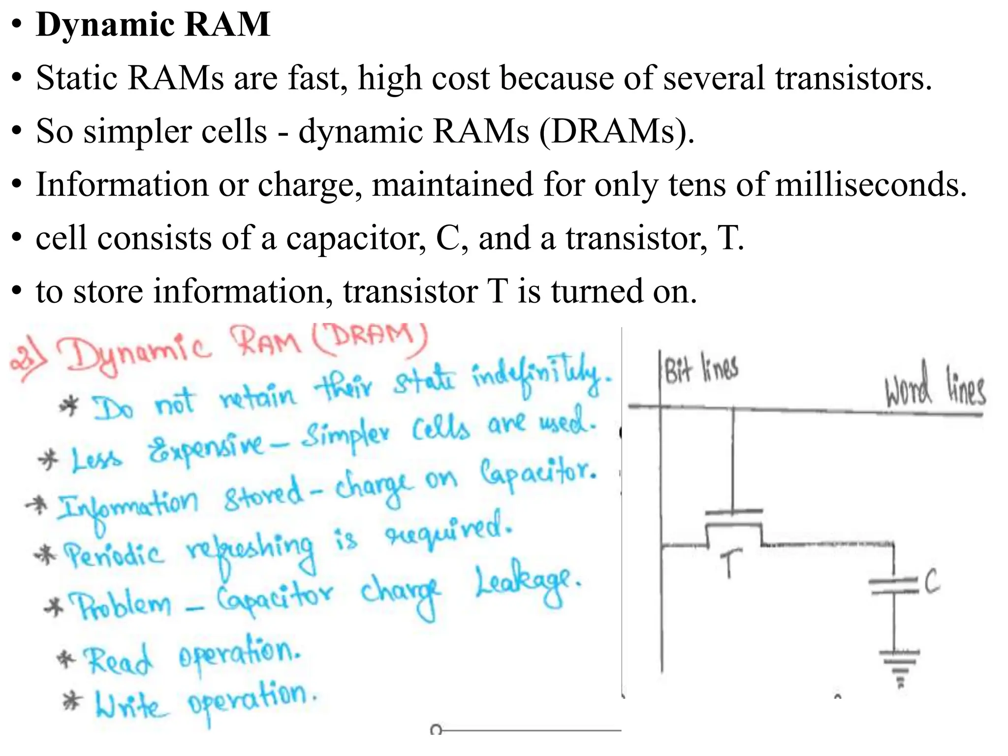
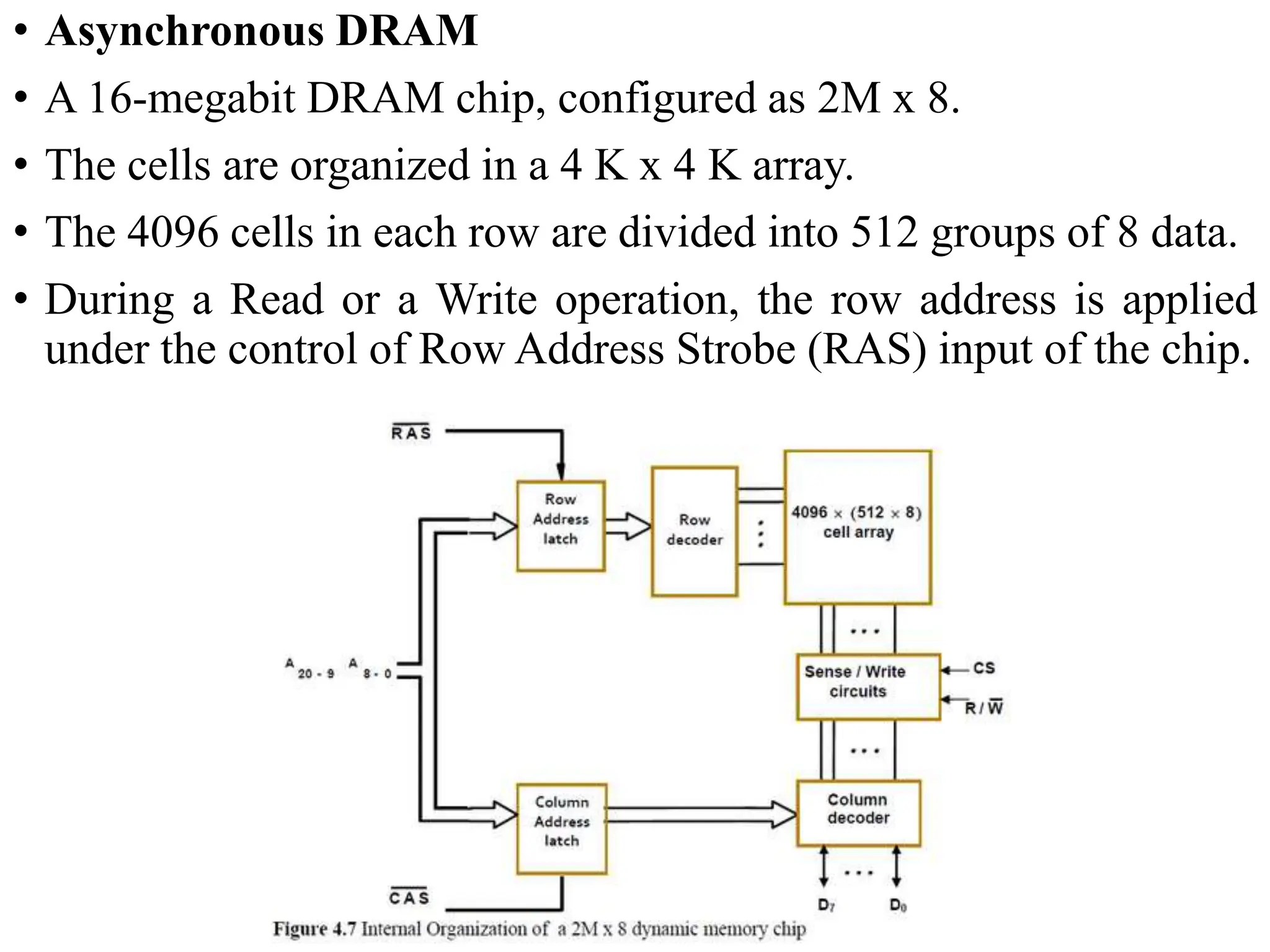
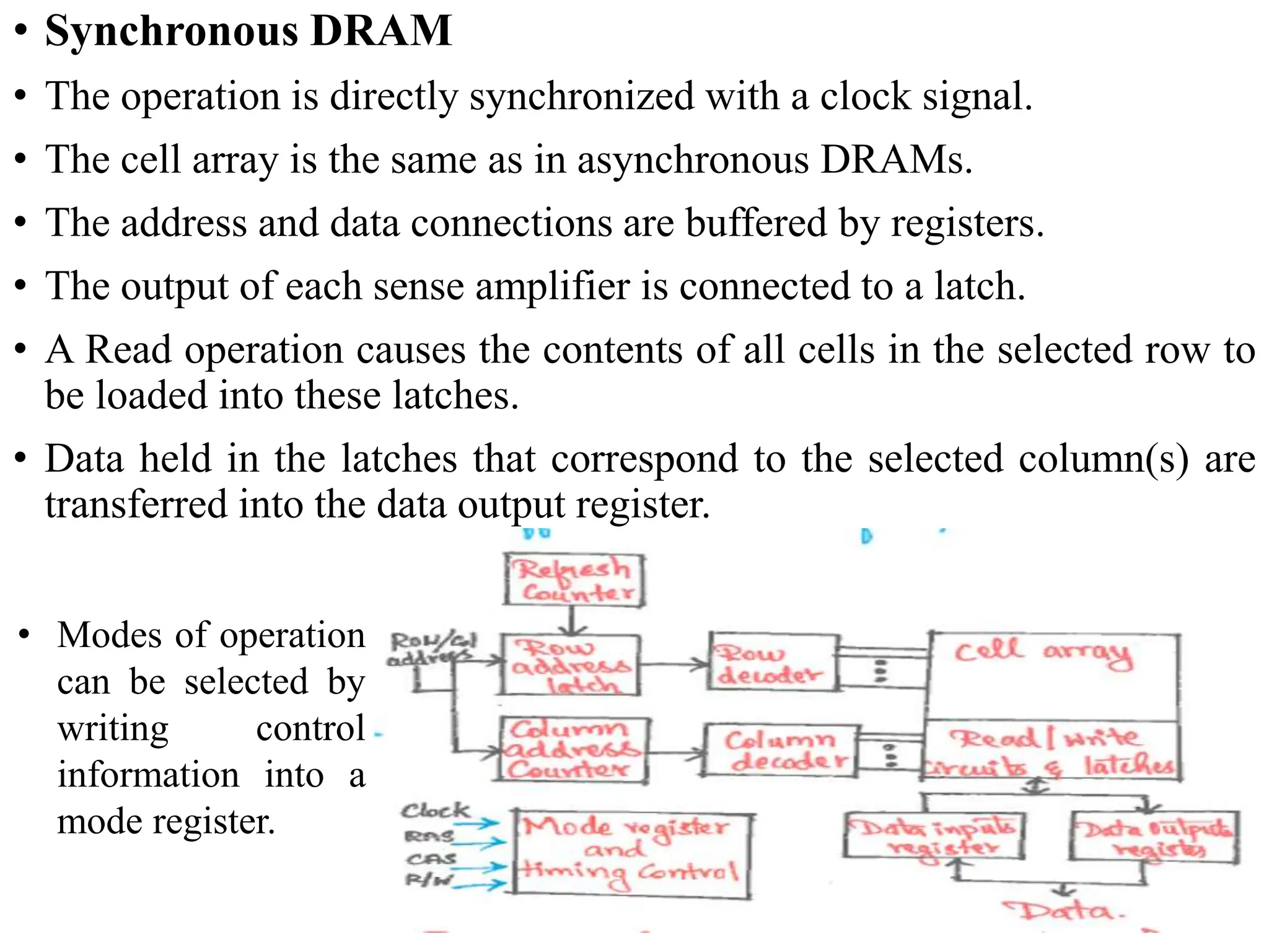
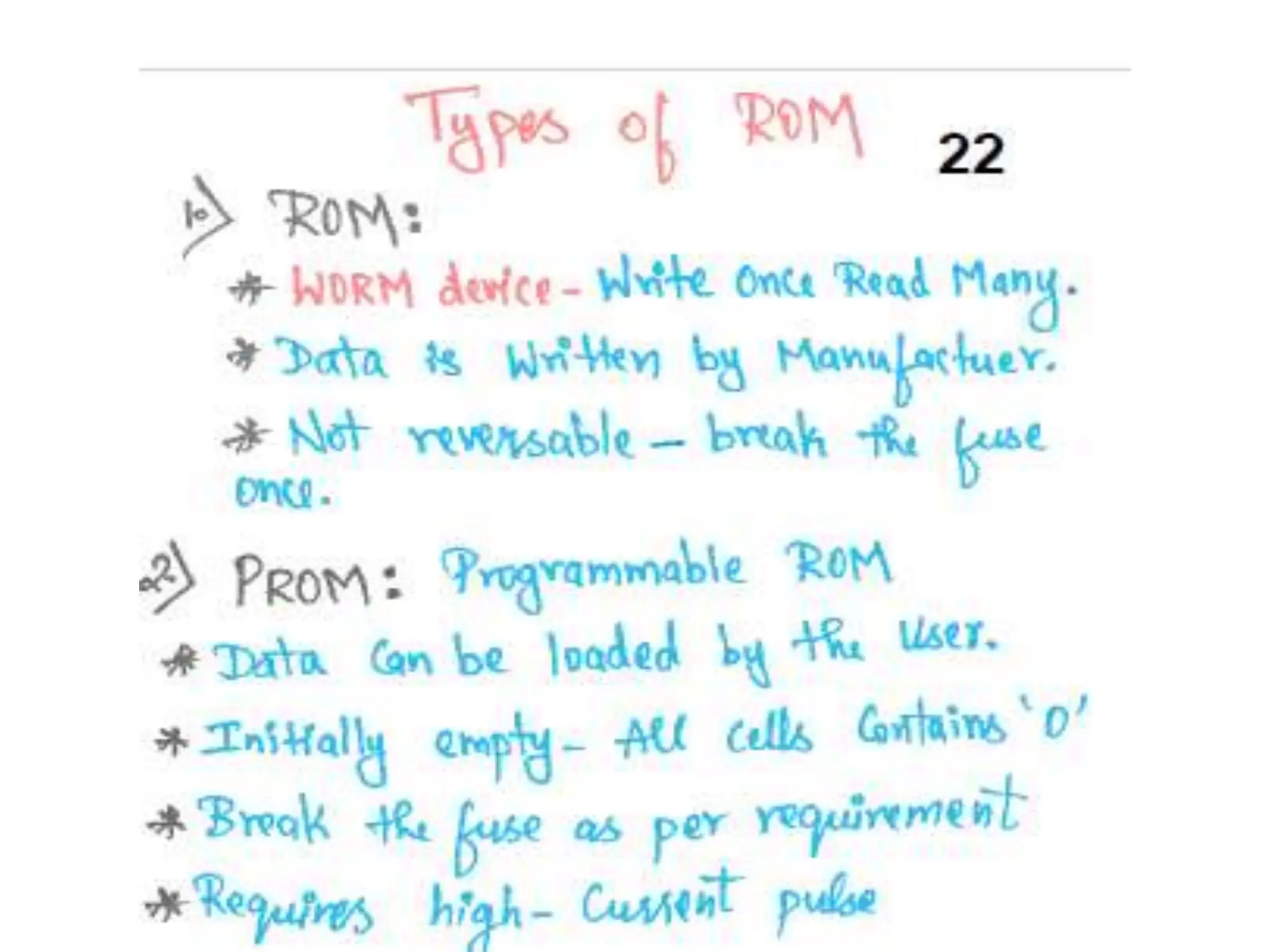
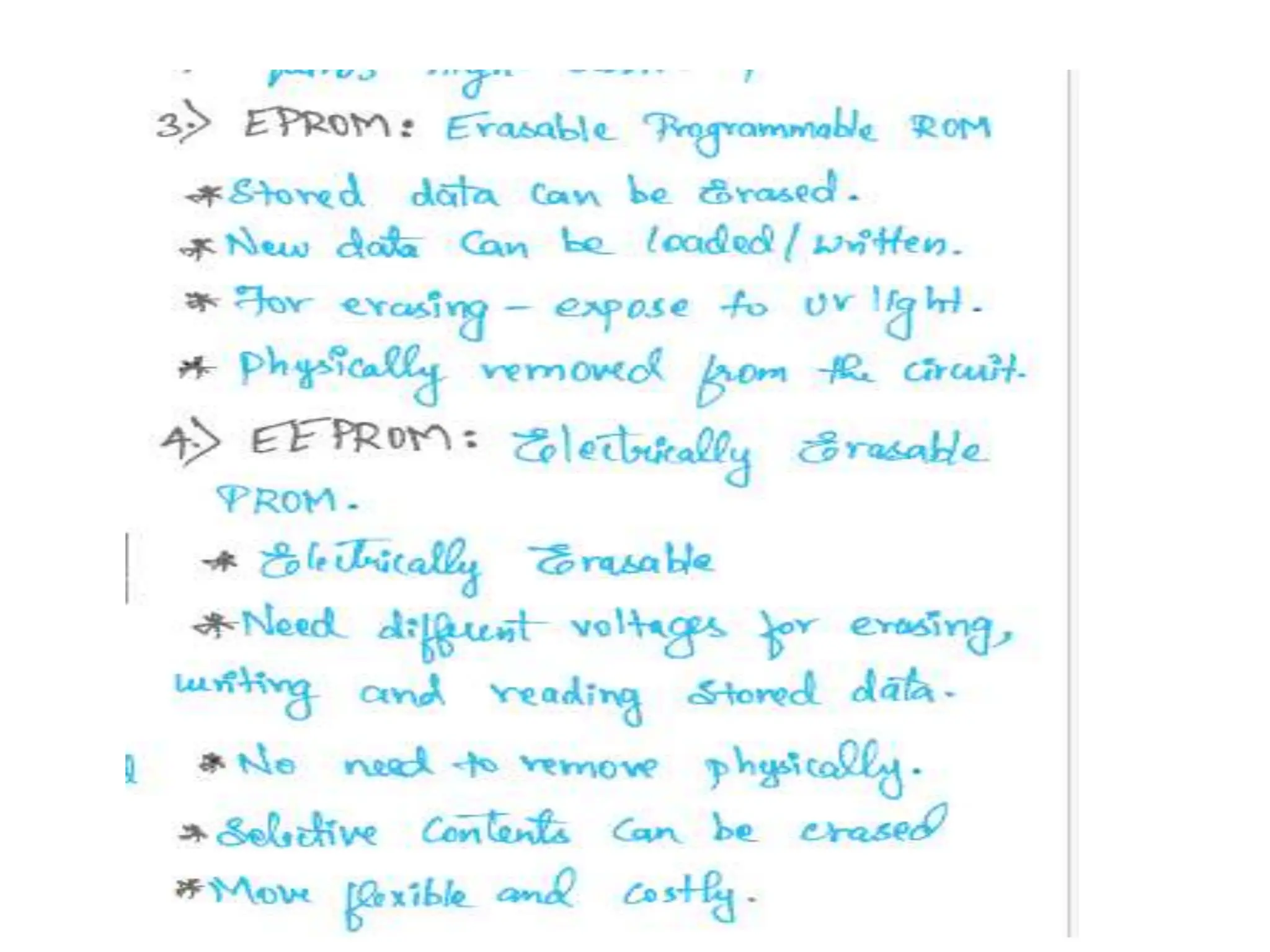
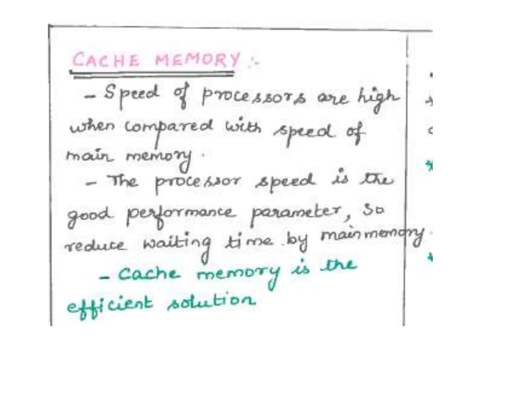
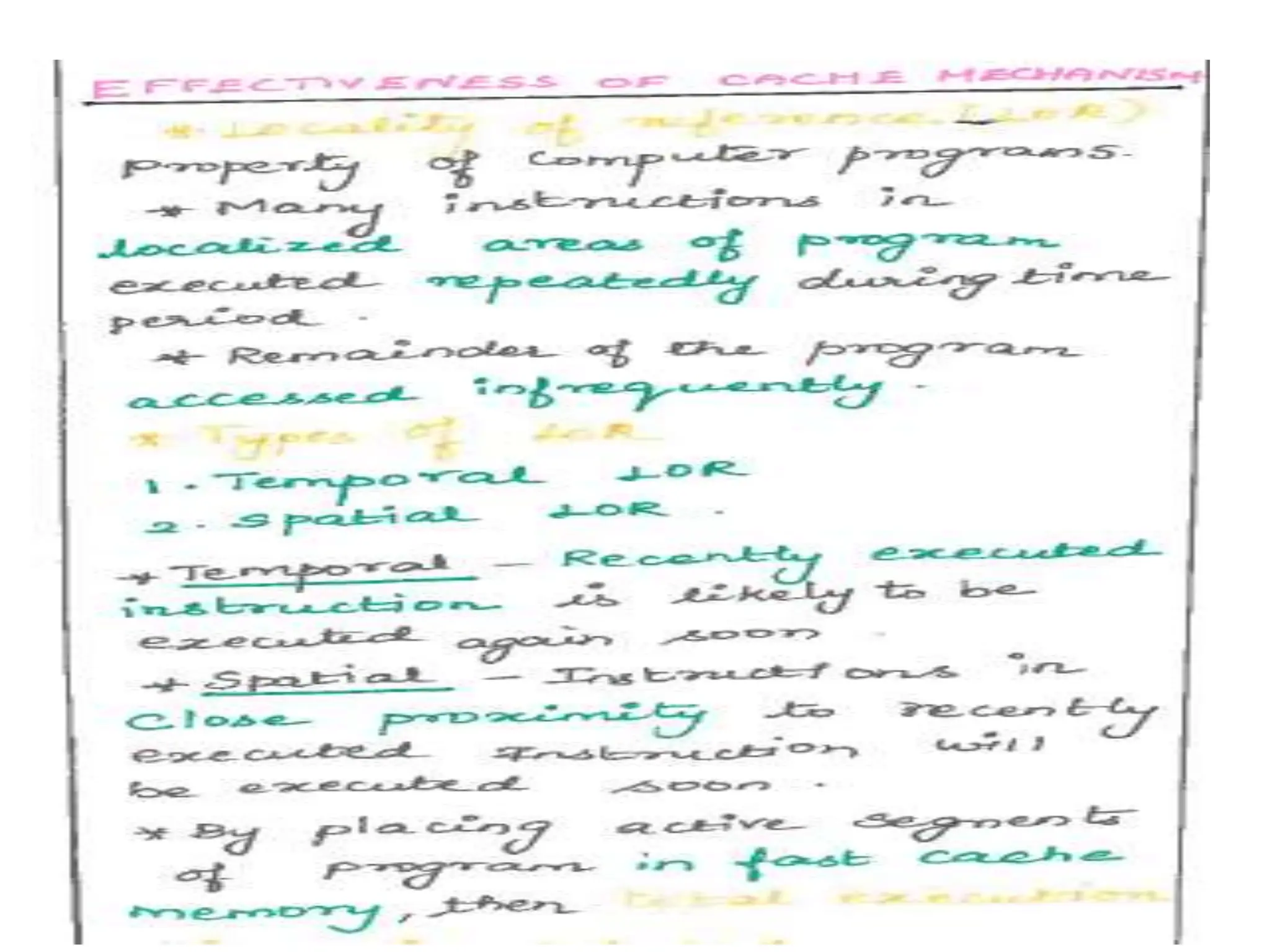
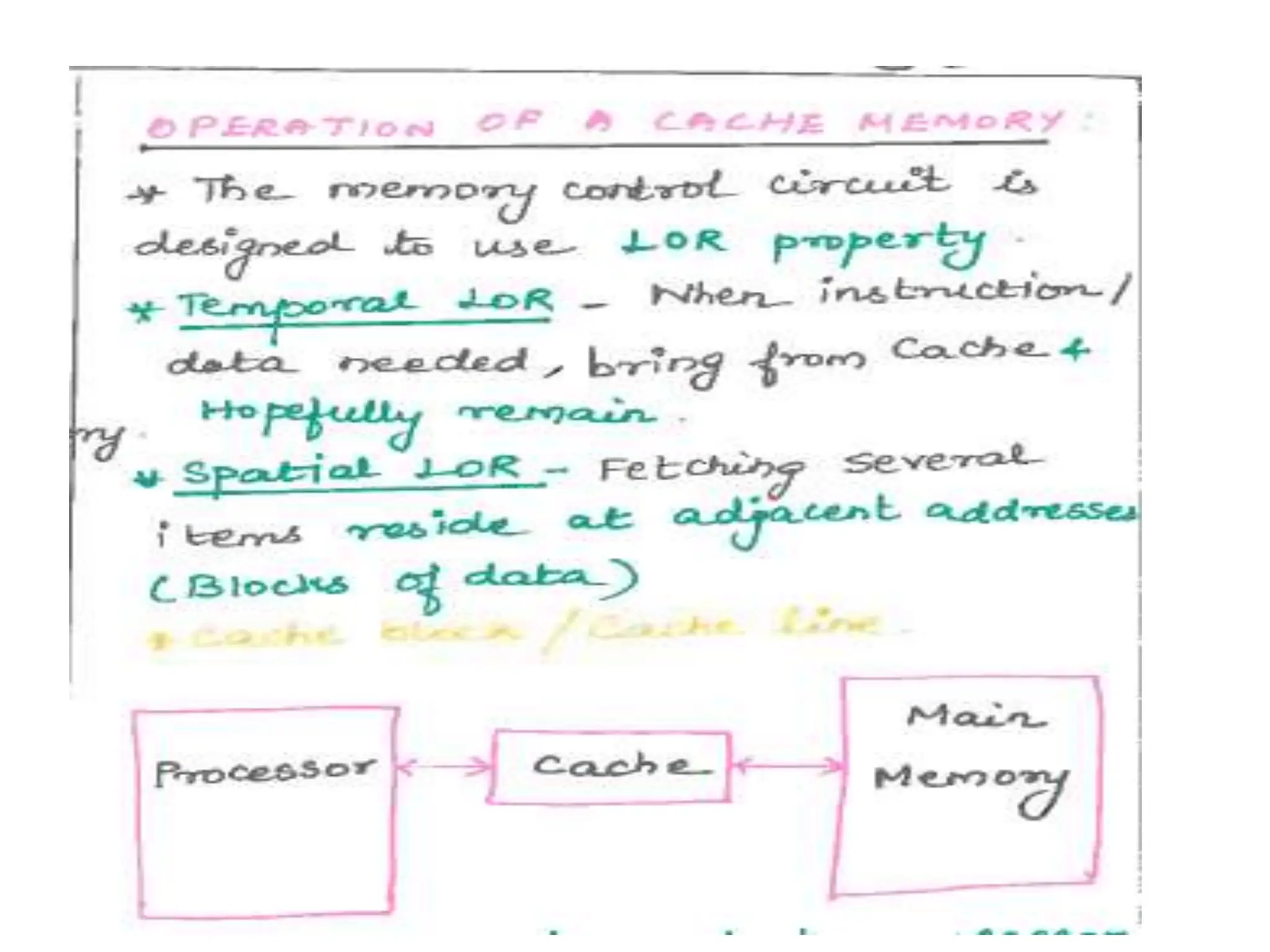
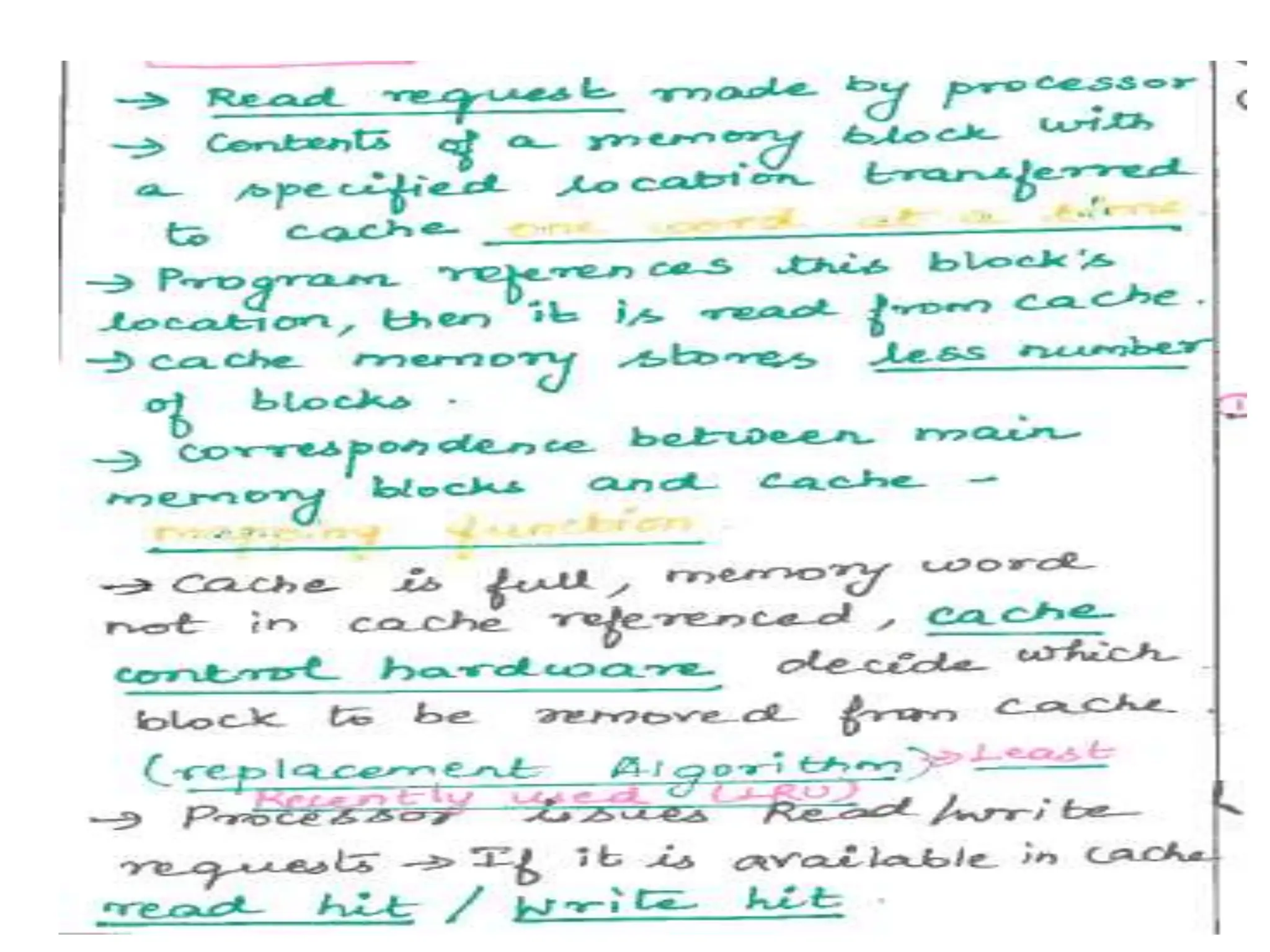
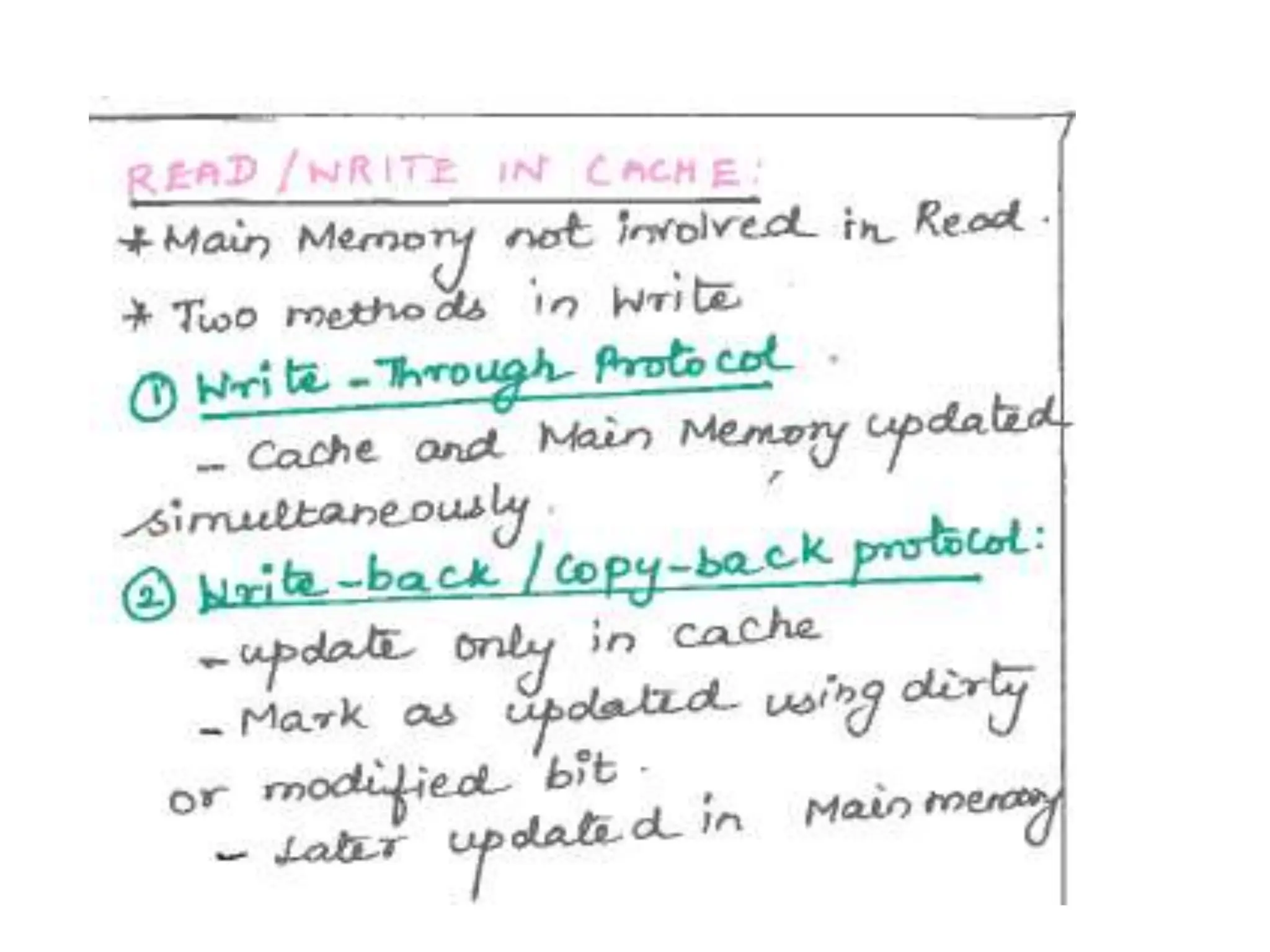
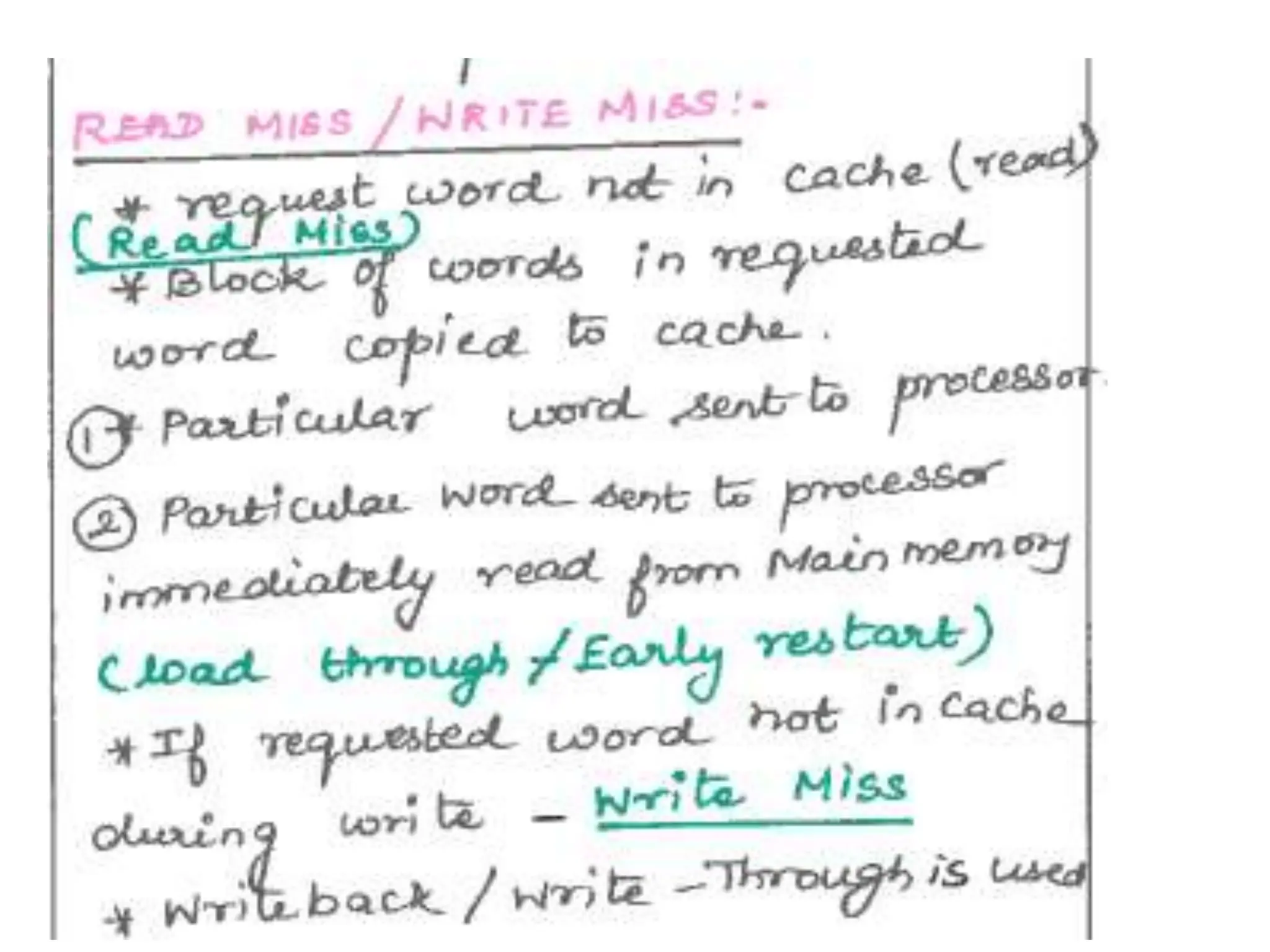
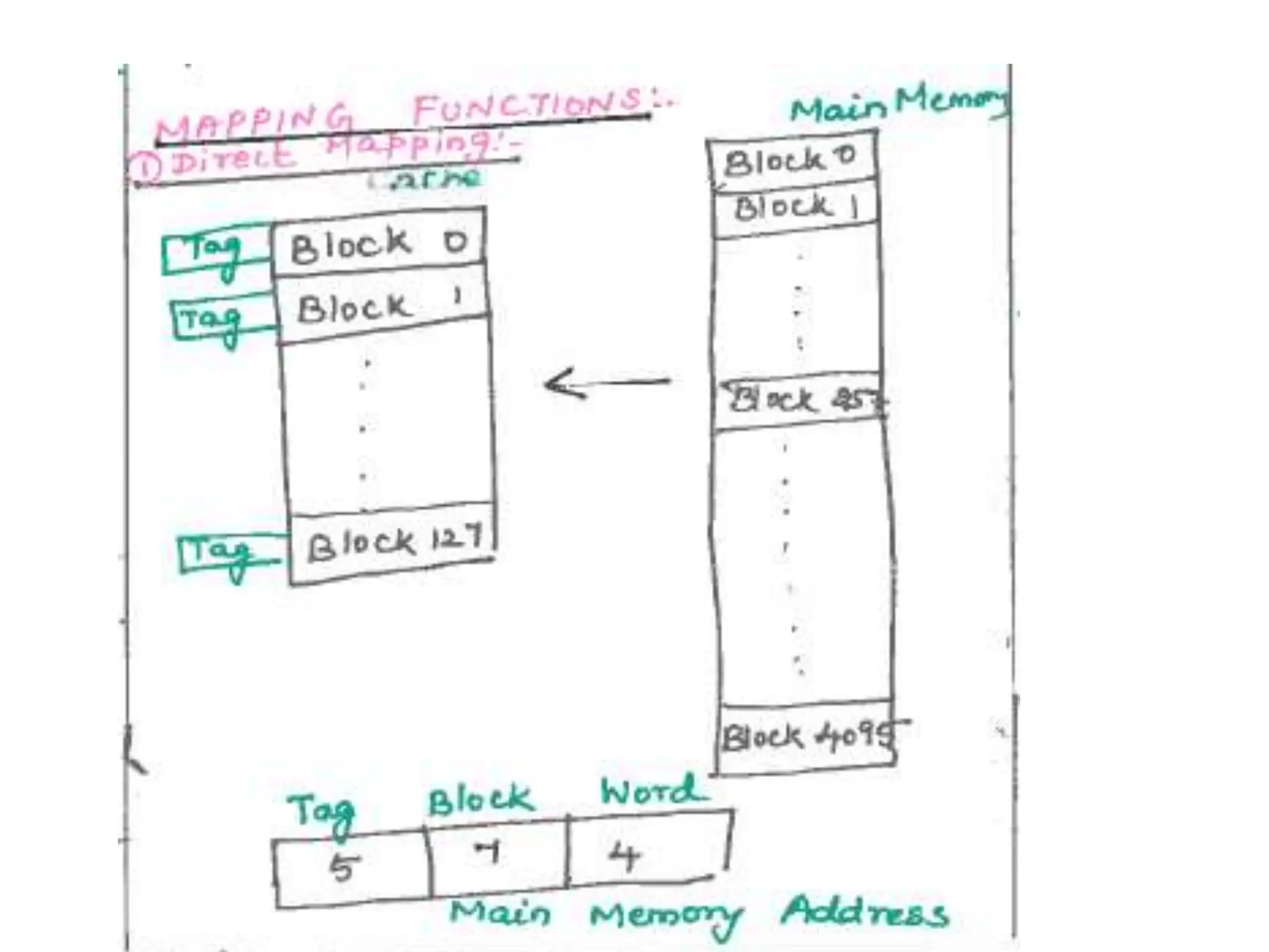
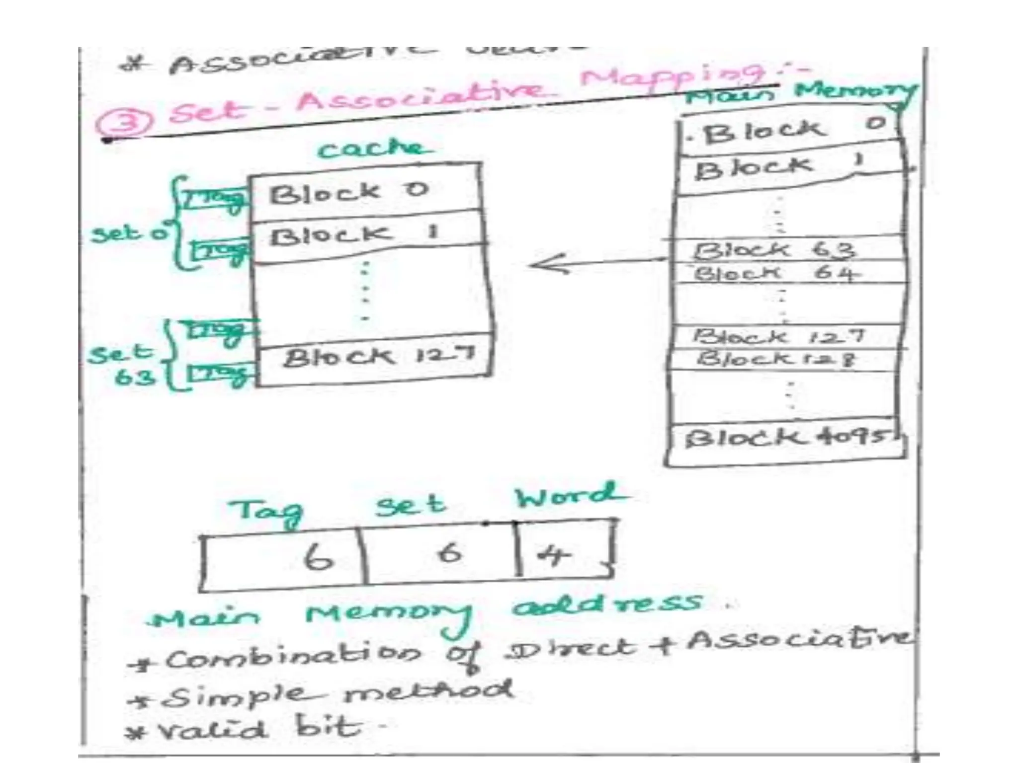
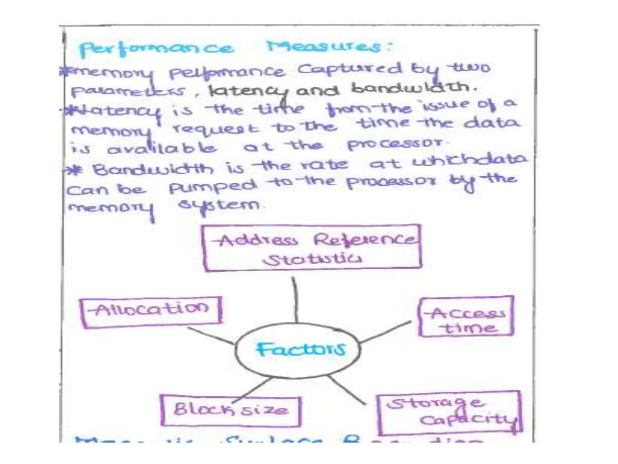
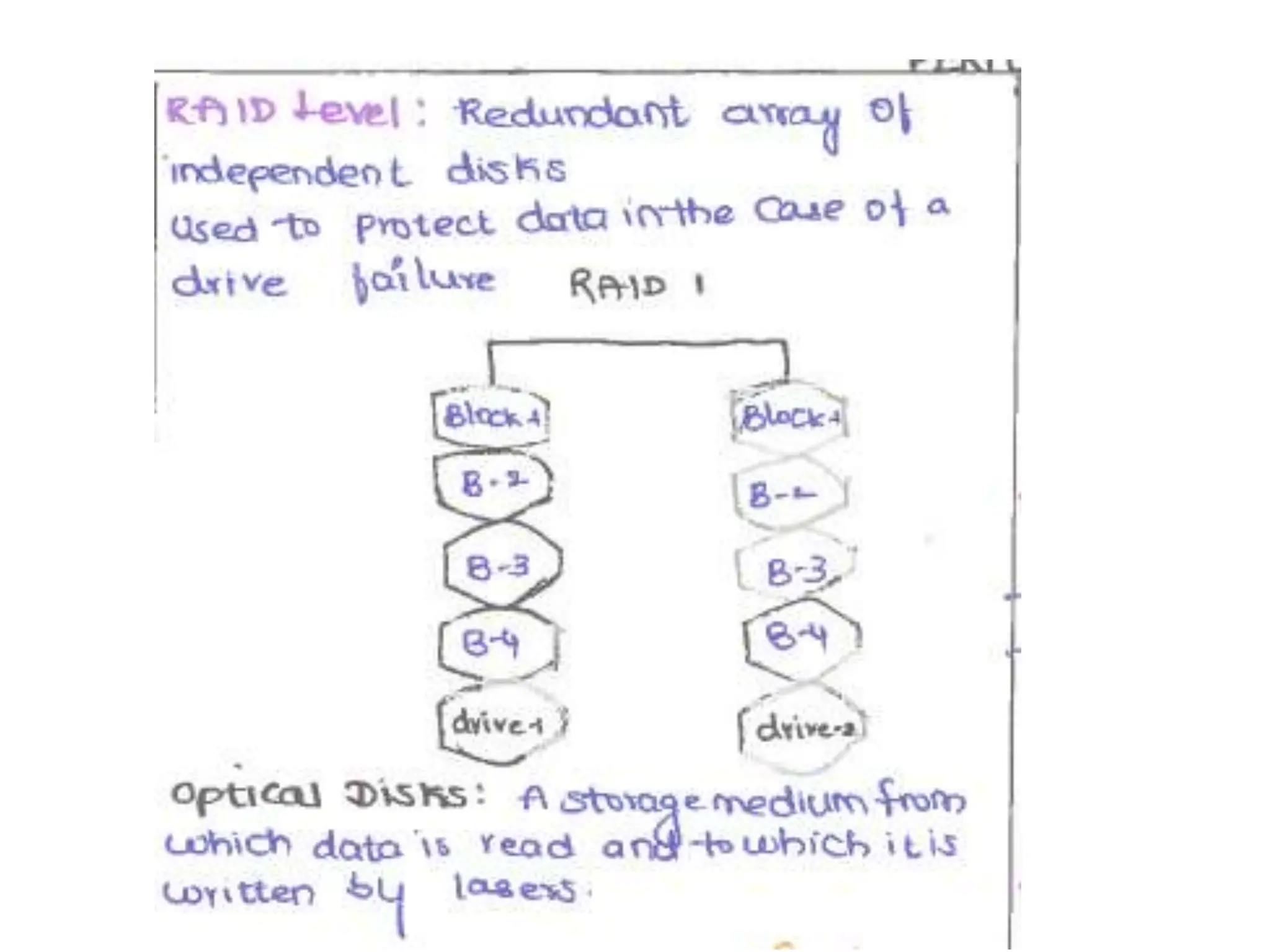
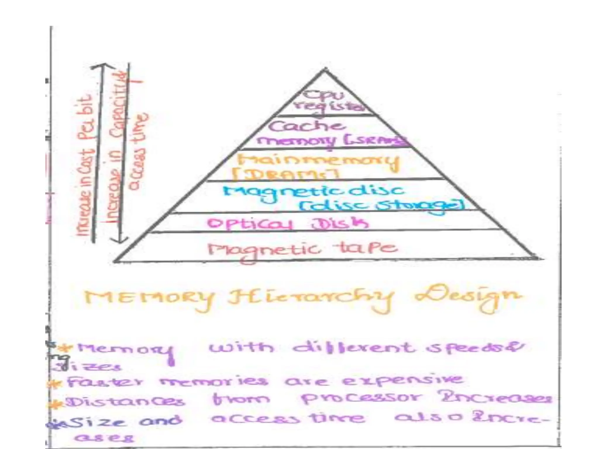
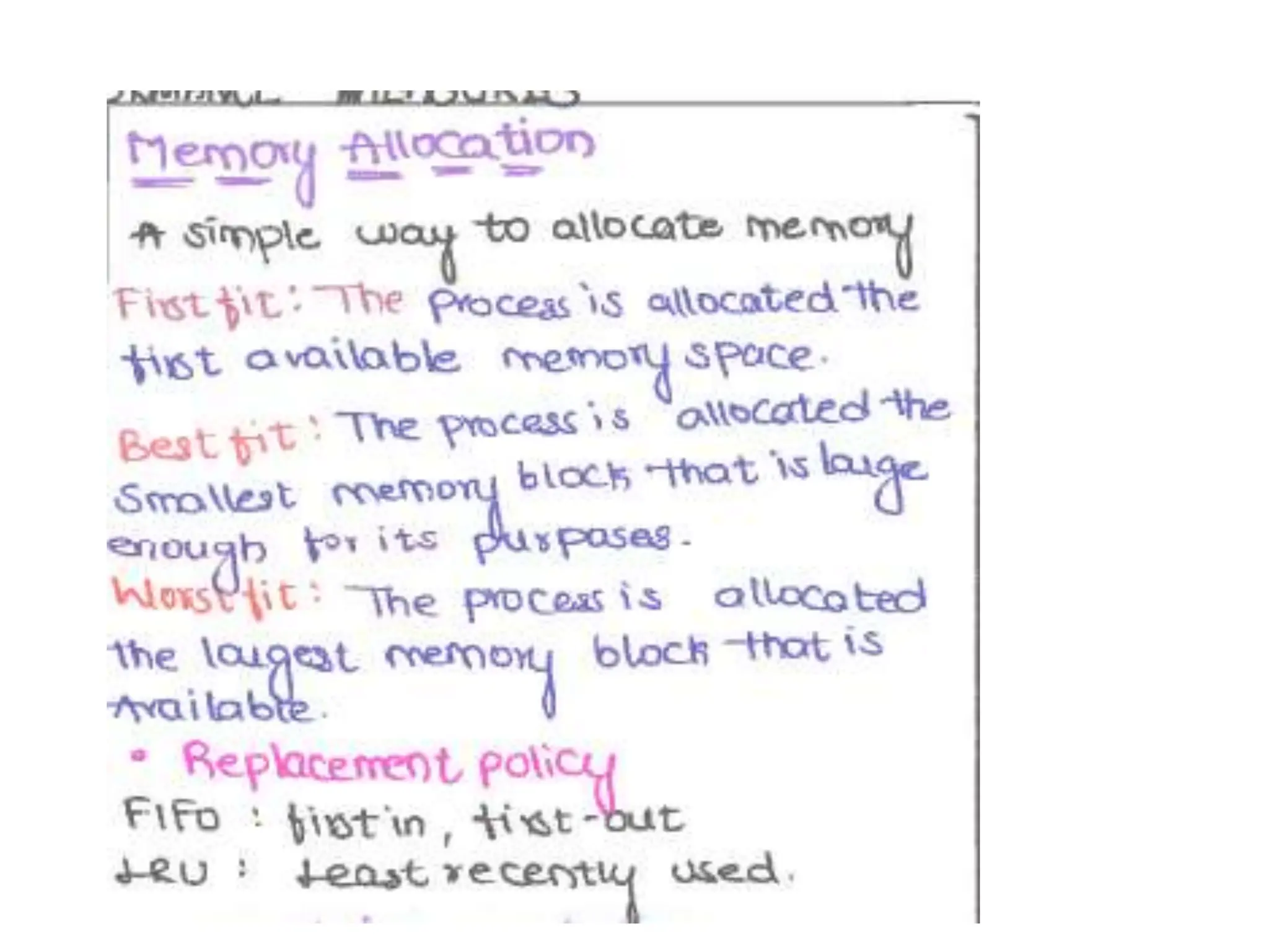
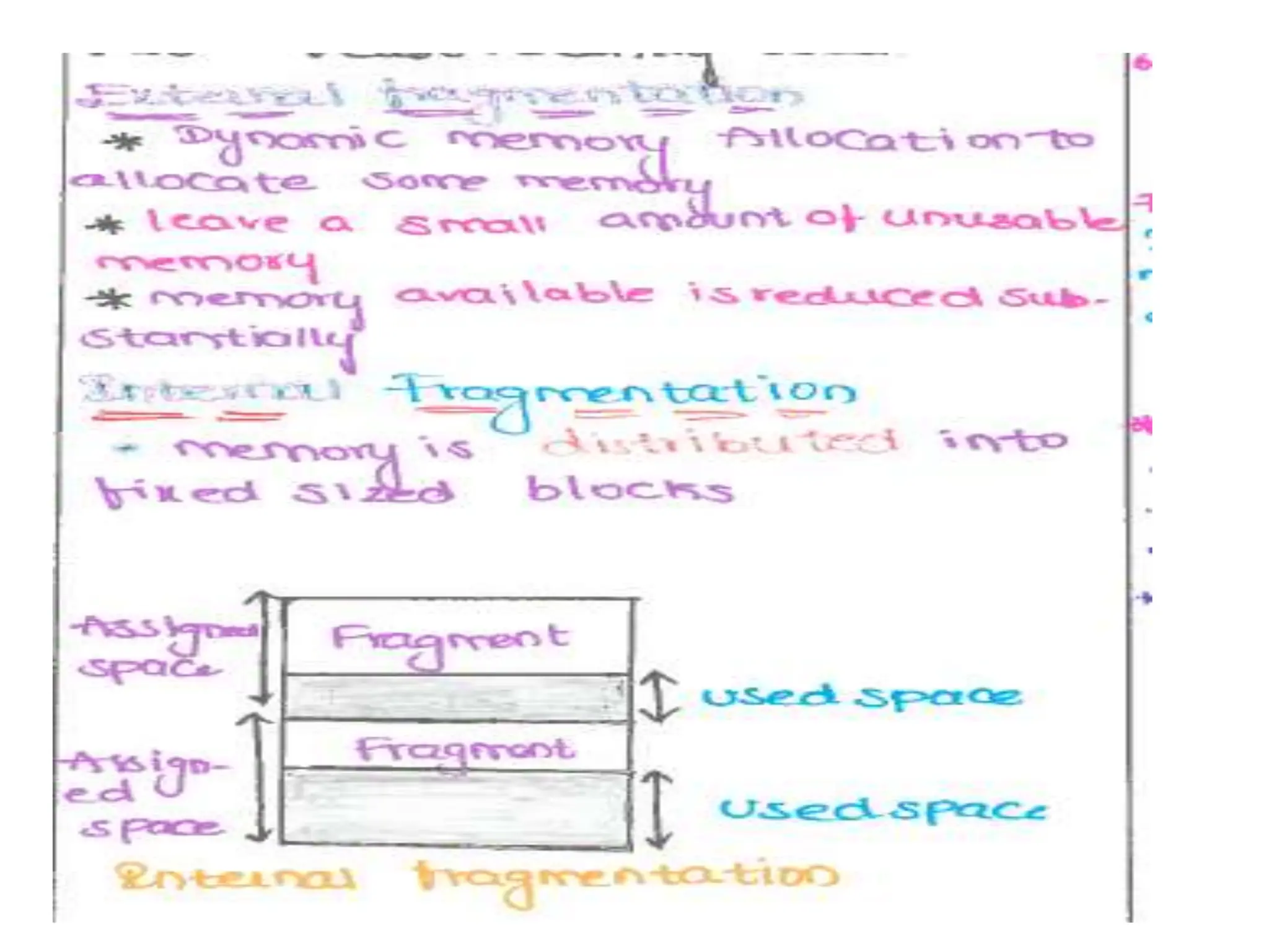
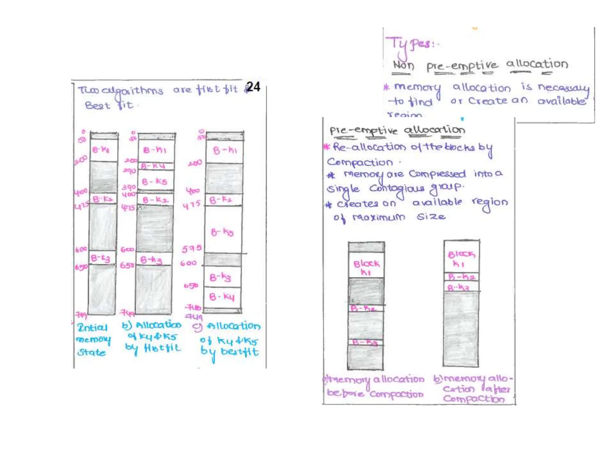
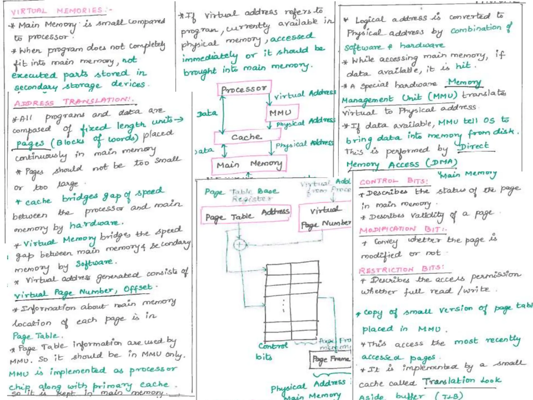
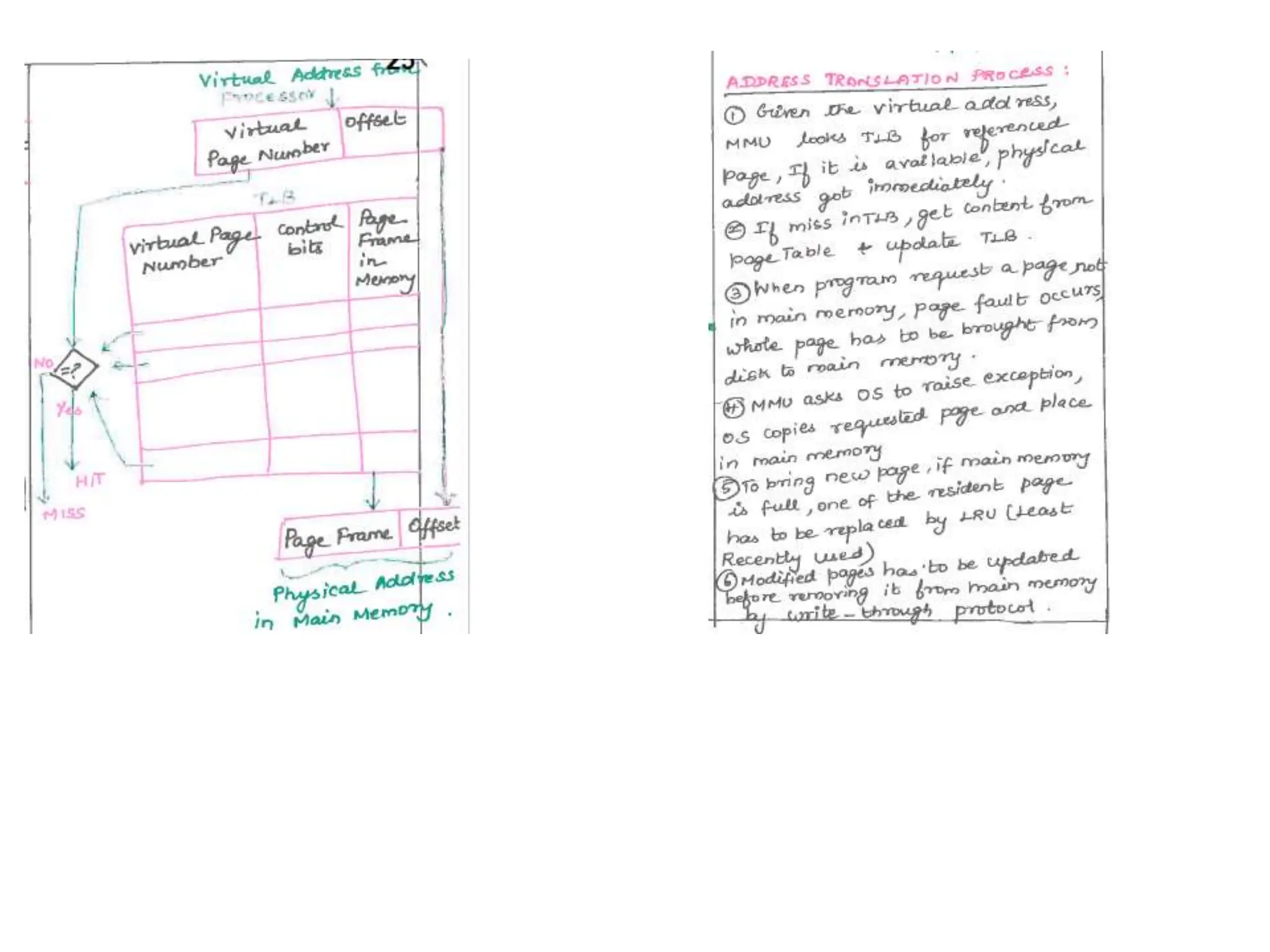
KEMBAR78
Unit- 4 Computer Oganization and Architecture | PPTX
Computer Architecture
UNIT IV MEMORY ORGANIZATION
Introduction - Random Access Memories - Read Only
Memory – Performance Measures – Memory
management requirements - Cache Memory – Virtual
Memory - Magnetic Surface Recording, Optical
Memories, Multilevel memories - Memory Allocation.
• Basic concepts of memory system - Introduction
• Computer memory,
• should have a large,
• facilitate execution of programs with huge amounts of data.
• should be fast, large, and inexpensive.
• but it is impossible to meet all three requirements.
• The maximum size of the memory,
• determined by the addressing scheme.
• For example, a 16-bit computer that generates 16-bit addresses
• addressing up to 216 = 64K (65536) memory locations.
• 32-bit addresses contains up to 232=4G (giga) memory
locations
• The number of locations represents the size of the address space.
• From the system point,
• memory unit as a black box.
• Data transfer through the use of two processor registers,
• (MAR and MDR).
• If MAR is k bits long and MDR is n bits long, then the memory
unit may contain up to 2k addressable locations.
• During a memory cycle, n bits of data are transferred.
• the processor bus has k address lines and n data lines.
• The bus also includes the control lines, Figure.
• Figure Connection of the memory to the processor
• The processor reads data by loading the address into the MAR,
• setting the R / W line to 1.
• The memory responds with data onto the data lines,
• by asserting the MFC signal.
• loads the data into the MDR register.
• The processor writes data by loading the address into MAR and
the data into MDR.
• setting the R/ W line to 0.
• The time between the Read and the MFC signals is referred to as
the memory access time.
• If any location can be accessed for a Read or Write operation
some fixed amount of time that is independent of the location's
address in a memory unit
• random-access memory (RAM).
• cache memory - to reduce the memory access time, small & fast.
• inserted between the larger, slower main memory and processor.
• Virtual memory, increase the size of the physical memory.
• Data are addressed in a virtual address space.
• active space is mapped onto locations in the physical memory.
• Random Access Memory
• Semiconductor memories are available in a wide range of speeds.
• Their cycle times range from l00ns to less than 10 ns.
• Random Access Memory • row of cells - a memory word, and
• cells of a row are connected to a
common line
• referred to as the word line,
• driven by the address decoder
on the chip.
• Sense/Write circuit,
• cells in each column are
connected
• data input/output lines of the
chip are connected.
• during a Read, circuit transmit
the information to the output
data lines.
• During a Write, the circuit
receive input and store it in the
cells.
• Types of RAM
• STATIC MEMORIES – Static RAM
• circuits retain their state as long as power is applied.
• two inverters are cross-connected to form a latch.
• latch is connected to two bit lines by transistors Tl and T2.
• These transistors act as switches.
• the cell is in state 1 if the logic value at X is 1 and Y is 0.
• Read operation
• If the cell is in state 1, the signal on bit line b is high and the
signal on bit line b' is low.
• The opposite is true if the cell is in state 0.
• Write operation
• if Tl and T2 are turned on (closed), it lines b and b' will have high
and low signals, respectively.
• Dynamic RAM
• Static RAMs are fast, high cost because of several transistors.
• So simpler cells - dynamic RAMs (DRAMs).
• Information or charge, maintained for only tens of milliseconds.
• cell consists of a capacitor, C, and a transistor, T.
• to store information, transistor T is turned on.
• Types of DRAMs
• RAS - Row Address Strobe
• CAS - Column Address Strobe
• Asynchronous DRAM
• A 16-megabit DRAM chip, configured as 2M x 8.
• The cells are organized in a 4 K x 4 K array.
• The 4096 cells in each row are divided into 512 groups of 8 data.
• During a Read or a Write operation, the row address is applied
under the control of Row Address Strobe (RAS) input of the chip.
• After the row address is loaded, the column address is loaded into
the column address latch under control of the Column Address
Strobe (CAS) signal.
• The information is decoded and the appropriate group of 8
Sense/Write circuits are selected.
• For a Read operation, the output values of the selected circuits are
transferred to the data lines, D7-0.
• For a Write operation, the information on the D7-0 lines is
transferred to the selected circuits.
• Synchronous DRAM
• The operation is directly synchronized with a clock signal.
• The cell array is the same as in asynchronous DRAMs.
• The address and data connections are buffered by registers.
• The output of each sense amplifier is connected to a latch.
• A Read operation causes the contents of all cells in the selected row to
be loaded into these latches.
• Data held in the latches that correspond to the selected column(s) are
transferred into the data output register.
• Modes of operation
can be selected by
writing control
information into a
mode register.
• http://www.faadooengineers.com/online-
study/post/cse/computer-organization-and-
architecture/496/process-fundamental-concepts

Unit- 4 Computer Oganization and Architecture

  • 1.
    Computer Architecture UNIT IVMEMORY ORGANIZATION Introduction - Random Access Memories - Read Only Memory – Performance Measures – Memory management requirements - Cache Memory – Virtual Memory - Magnetic Surface Recording, Optical Memories, Multilevel memories - Memory Allocation.
  • 2.
    • Basic conceptsof memory system - Introduction • Computer memory, • should have a large, • facilitate execution of programs with huge amounts of data. • should be fast, large, and inexpensive. • but it is impossible to meet all three requirements. • The maximum size of the memory, • determined by the addressing scheme. • For example, a 16-bit computer that generates 16-bit addresses • addressing up to 216 = 64K (65536) memory locations. • 32-bit addresses contains up to 232=4G (giga) memory locations • The number of locations represents the size of the address space.
  • 3.
    • From thesystem point, • memory unit as a black box. • Data transfer through the use of two processor registers, • (MAR and MDR). • If MAR is k bits long and MDR is n bits long, then the memory unit may contain up to 2k addressable locations. • During a memory cycle, n bits of data are transferred. • the processor bus has k address lines and n data lines. • The bus also includes the control lines, Figure. • Figure Connection of the memory to the processor
  • 4.
    • The processorreads data by loading the address into the MAR, • setting the R / W line to 1. • The memory responds with data onto the data lines, • by asserting the MFC signal. • loads the data into the MDR register. • The processor writes data by loading the address into MAR and the data into MDR. • setting the R/ W line to 0.
  • 5.
    • The timebetween the Read and the MFC signals is referred to as the memory access time. • If any location can be accessed for a Read or Write operation some fixed amount of time that is independent of the location's address in a memory unit • random-access memory (RAM). • cache memory - to reduce the memory access time, small & fast. • inserted between the larger, slower main memory and processor. • Virtual memory, increase the size of the physical memory. • Data are addressed in a virtual address space. • active space is mapped onto locations in the physical memory.
  • 6.
    • Random AccessMemory • Semiconductor memories are available in a wide range of speeds. • Their cycle times range from l00ns to less than 10 ns.
  • 7.
    • Random AccessMemory • row of cells - a memory word, and • cells of a row are connected to a common line • referred to as the word line, • driven by the address decoder on the chip. • Sense/Write circuit, • cells in each column are connected • data input/output lines of the chip are connected. • during a Read, circuit transmit the information to the output data lines. • During a Write, the circuit receive input and store it in the cells.
  • 8.
  • 9.
    • STATIC MEMORIES– Static RAM • circuits retain their state as long as power is applied. • two inverters are cross-connected to form a latch. • latch is connected to two bit lines by transistors Tl and T2. • These transistors act as switches. • the cell is in state 1 if the logic value at X is 1 and Y is 0. • Read operation • If the cell is in state 1, the signal on bit line b is high and the signal on bit line b' is low. • The opposite is true if the cell is in state 0. • Write operation • if Tl and T2 are turned on (closed), it lines b and b' will have high and low signals, respectively.
  • 10.
    • Dynamic RAM •Static RAMs are fast, high cost because of several transistors. • So simpler cells - dynamic RAMs (DRAMs). • Information or charge, maintained for only tens of milliseconds. • cell consists of a capacitor, C, and a transistor, T. • to store information, transistor T is turned on.
  • 11.
    • Types ofDRAMs • RAS - Row Address Strobe • CAS - Column Address Strobe
  • 12.
    • Asynchronous DRAM •A 16-megabit DRAM chip, configured as 2M x 8. • The cells are organized in a 4 K x 4 K array. • The 4096 cells in each row are divided into 512 groups of 8 data. • During a Read or a Write operation, the row address is applied under the control of Row Address Strobe (RAS) input of the chip.
  • 13.
    • After therow address is loaded, the column address is loaded into the column address latch under control of the Column Address Strobe (CAS) signal. • The information is decoded and the appropriate group of 8 Sense/Write circuits are selected. • For a Read operation, the output values of the selected circuits are transferred to the data lines, D7-0. • For a Write operation, the information on the D7-0 lines is transferred to the selected circuits.
  • 14.
    • Synchronous DRAM •The operation is directly synchronized with a clock signal. • The cell array is the same as in asynchronous DRAMs. • The address and data connections are buffered by registers. • The output of each sense amplifier is connected to a latch. • A Read operation causes the contents of all cells in the selected row to be loaded into these latches. • Data held in the latches that correspond to the selected column(s) are transferred into the data output register. • Modes of operation can be selected by writing control information into a mode register.
  • 39.