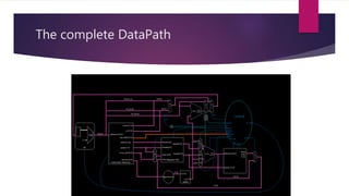
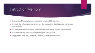
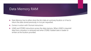
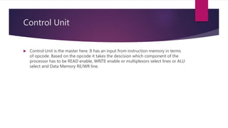
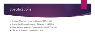
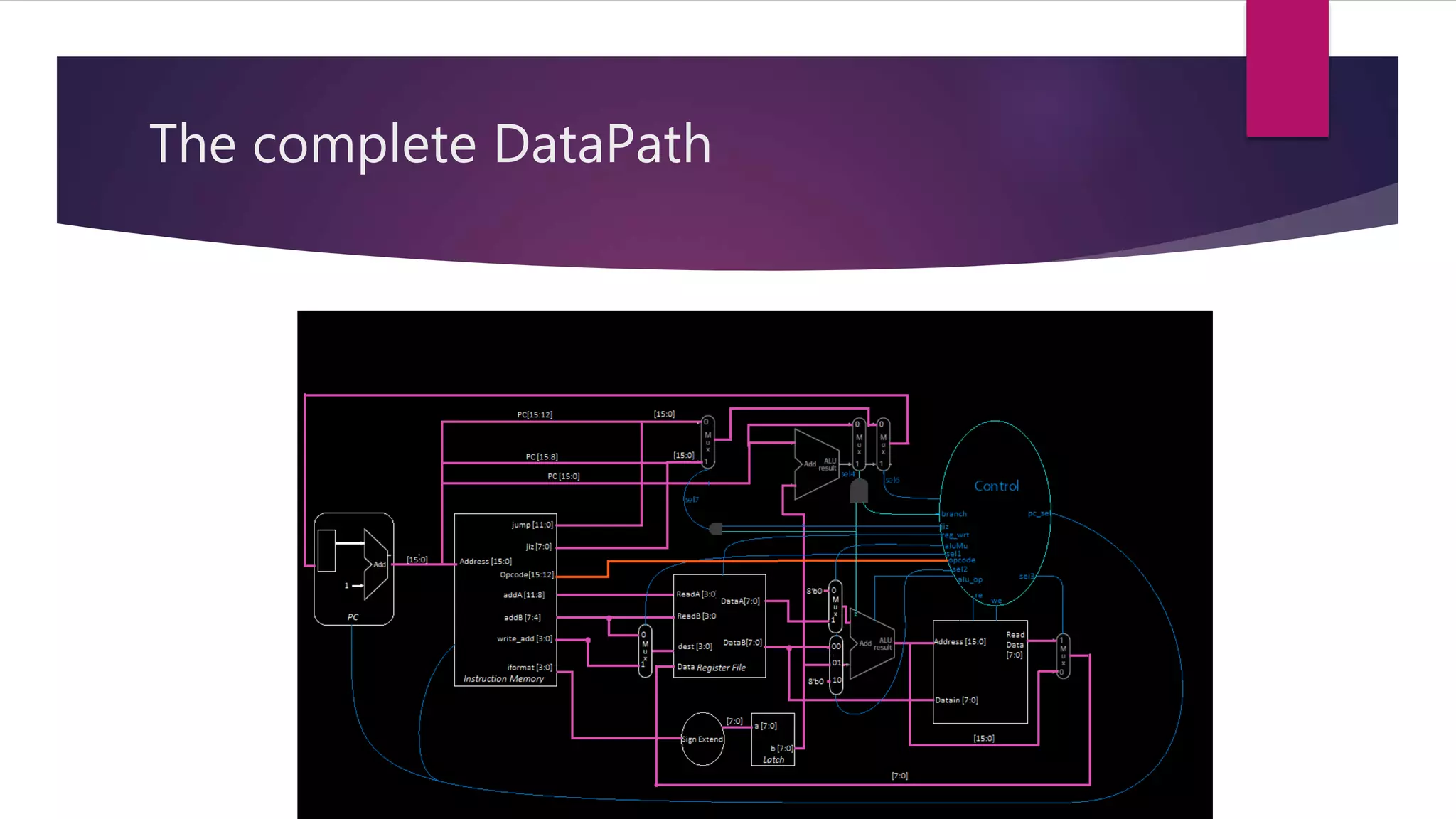
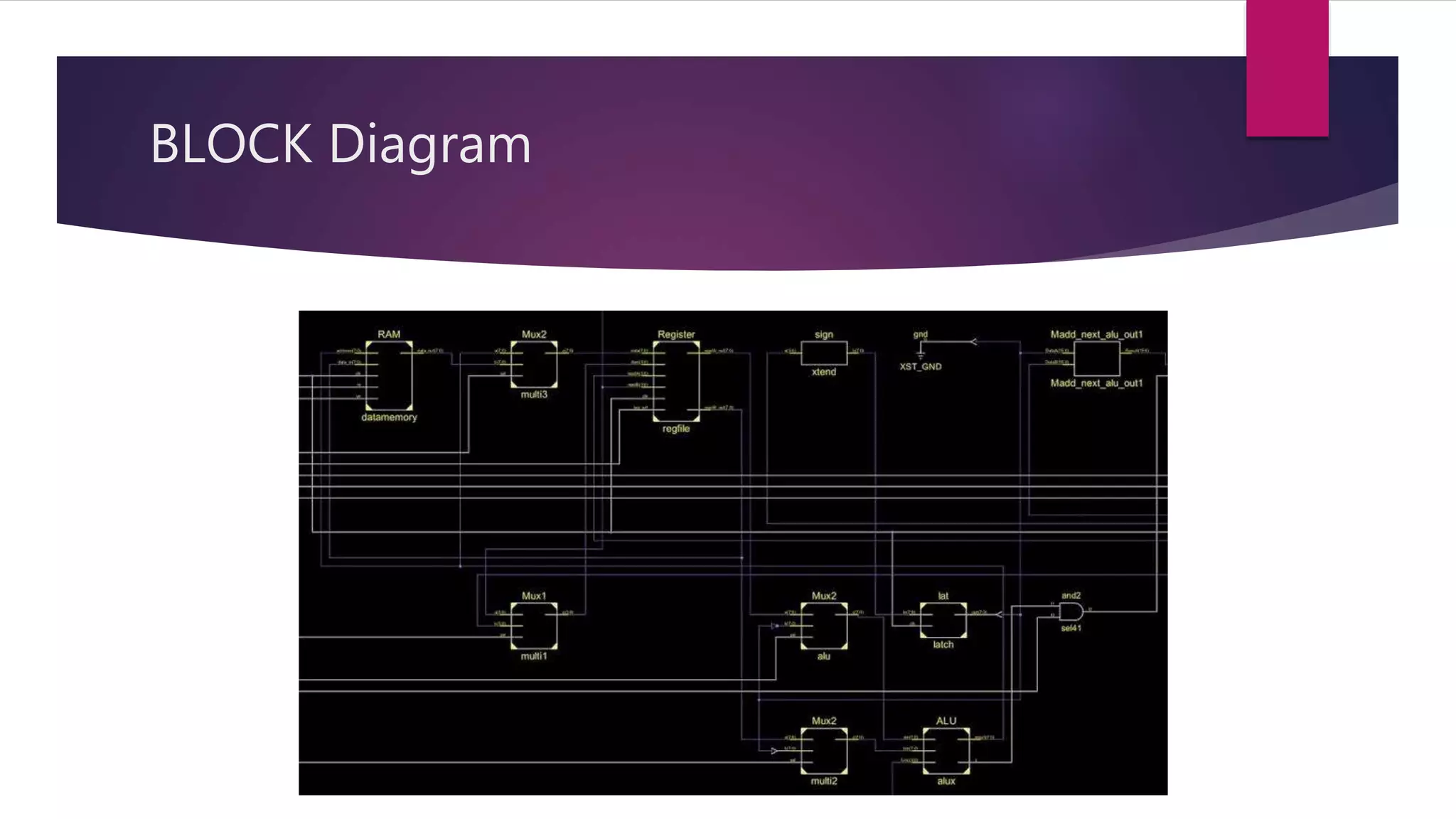
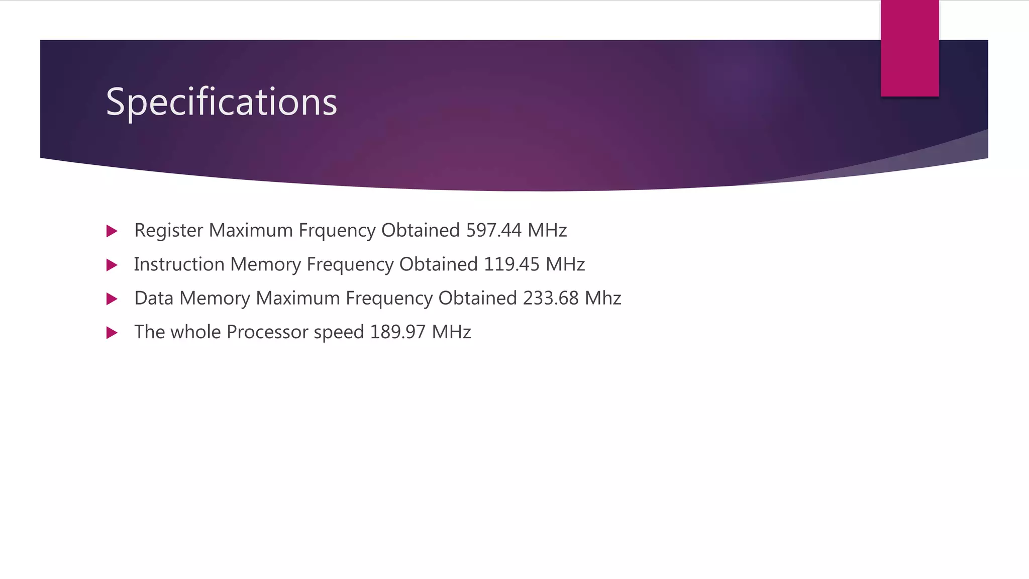
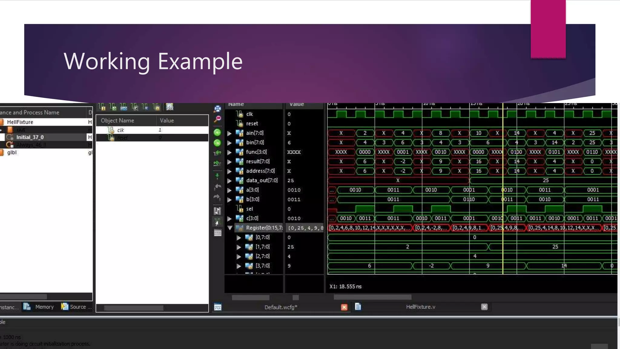
KEMBAR78
16bit RISC Processor | PPTX
16bit RISC Processor
VISIT THIS LINK (WWW.HELLOCODINGS.COM) FOR COMPLETE CODE
Contents
 Data Path of Processor
 BLOCK Diagram
 Why RISC?
 ALU
 Program Counter
 Instruction Memory
 RAM
 Multiplexors
 Register
 Control Unit
The complete DataPath
BLOCK Diagram
RISC
 Why was RISC introduced ?
 As compared with CISC (Complex Instruction Set Computer) which takes a
complex time to execute the instructions was reducing the performance of
computing where the speed was drowning when CPU contacts the data memory.
Hence another alternative was set in motion and that was RISC architecture.
ALU Arithmetic Logical Unit
 Arithmetic Logic Unit compiles the arithmetic operation, logical operations.
 Arithmetic Operations can be counted as addition, subtraction etc.
 Logical Operations are like AND, OR, NAND between two binary numbers
 Operations depends on the opcode from the control unit.
 It takes 2 clock cycles to process data
 Code for ALU here HERE
Program Counter
 Program counter has to update the counter which points to the location of next
instruction. It will get updated as soon as the prior instruction is executed.
 Program Counter location can be changed by the opcode provided like that of
JUMP instructions etc.
 Code for Program Counter is HERE
Instruction Memory
 Instruction Memory has an instruction length of 16 bits here.
 It holds the information or better say the instruction that has to be performed
successively.
 As soon as the instruction is executed new instruction loaded into memory.
 Can execute any instruction depending on the opcode.
 Support for JMP, BEQ, Iformat, J-format, J-format instruction
Data Memory RAM
 Data Memory has to either store the ALU data at a primary location or it has to
return the data stored previously in it as per requested.
 Comes in action with I format instructions
 LOAD and STORE instructions access the data memory. When LOAD is required
data from a location in retrieved and when STORE I loaded data is loader or
written at the location provided.
Multiplexors
 Multiplexors have been used here to decide the JUMP location, Register Location
to write and Arithmetic input. It is also used to select the address to new location
in instruction memory.
 Select Lines are controlled by Control Unit.
Control Unit
 Control Unit is the master here. It has an input from instruction memory in terms
of opcode. Based on the opcode it takes the descision which component of the
processor has to be READ enable, WRITE enable or multiplexors select lines or ALU
select and Data Memory RE/WR line.
Specifications
 Register Maximum Frquency Obtained 597.44 MHz
 Instruction Memory Frequency Obtained 119.45 MHz
 Data Memory Maximum Frequency Obtained 233.68 Mhz
 The whole Processor speed 189.97 MHz
Working Example
Thank You
 Visit Here for the project and feel free to comment
 Sharing Knowledge 

16bit RISC Processor

  • 1.
    16bit RISC Processor VISITTHIS LINK (WWW.HELLOCODINGS.COM) FOR COMPLETE CODE
  • 2.
    Contents  Data Pathof Processor  BLOCK Diagram  Why RISC?  ALU  Program Counter  Instruction Memory  RAM  Multiplexors  Register  Control Unit
  • 3.
  • 4.
  • 5.
    RISC  Why wasRISC introduced ?  As compared with CISC (Complex Instruction Set Computer) which takes a complex time to execute the instructions was reducing the performance of computing where the speed was drowning when CPU contacts the data memory. Hence another alternative was set in motion and that was RISC architecture.
  • 6.
    ALU Arithmetic LogicalUnit  Arithmetic Logic Unit compiles the arithmetic operation, logical operations.  Arithmetic Operations can be counted as addition, subtraction etc.  Logical Operations are like AND, OR, NAND between two binary numbers  Operations depends on the opcode from the control unit.  It takes 2 clock cycles to process data  Code for ALU here HERE
  • 7.
    Program Counter  Programcounter has to update the counter which points to the location of next instruction. It will get updated as soon as the prior instruction is executed.  Program Counter location can be changed by the opcode provided like that of JUMP instructions etc.  Code for Program Counter is HERE
  • 8.
    Instruction Memory  InstructionMemory has an instruction length of 16 bits here.  It holds the information or better say the instruction that has to be performed successively.  As soon as the instruction is executed new instruction loaded into memory.  Can execute any instruction depending on the opcode.  Support for JMP, BEQ, Iformat, J-format, J-format instruction
  • 9.
    Data Memory RAM Data Memory has to either store the ALU data at a primary location or it has to return the data stored previously in it as per requested.  Comes in action with I format instructions  LOAD and STORE instructions access the data memory. When LOAD is required data from a location in retrieved and when STORE I loaded data is loader or written at the location provided.
  • 10.
    Multiplexors  Multiplexors havebeen used here to decide the JUMP location, Register Location to write and Arithmetic input. It is also used to select the address to new location in instruction memory.  Select Lines are controlled by Control Unit.
  • 11.
    Control Unit  ControlUnit is the master here. It has an input from instruction memory in terms of opcode. Based on the opcode it takes the descision which component of the processor has to be READ enable, WRITE enable or multiplexors select lines or ALU select and Data Memory RE/WR line.
  • 12.
    Specifications  Register MaximumFrquency Obtained 597.44 MHz  Instruction Memory Frequency Obtained 119.45 MHz  Data Memory Maximum Frequency Obtained 233.68 Mhz  The whole Processor speed 189.97 MHz
  • 13.
  • 14.
    Thank You  VisitHere for the project and feel free to comment  Sharing Knowledge 