KEMBAR78
Arrow multisolution nxp lpc4300 dual core | PPT
LPC4300 Cortex-M4 +M0 Dual Core
Microcontrollers
Arrow Israel
Amir Sherman
Semiconductors Technical Manager
NXP is a leader in ARM Flash MCUs
Clear strategy: 100% focus on ARM
Top performance through leading
technology & architecture
Design flexibility through pin- and
software-compatible solutions
– Scalable memory sizes
– Widest range of peripherals
Unlimited choice through complete
families for multiple cores
Cortex
M4
Cortex
M3
Cortex
M0
ARM7
ARM9
8051
32-bit16-bit8-bit
NXP Changing Microcontroller Landscape
DSP
cost performance
Very low-end 8b
e.g. 6-8 pin
not planned
High-end
DSP/MPU not
planned
ARM Cortex-M Continuum
Cortex-M4Cortex-M3Cortex-M0
Breaking through traditional boundaries of 8b, 16b, 32b and DSP
The ONLY vendor that offers the full range of ARM Cortex-M microcontroller families
Binary and tool compatible
Cortex-M Processors: Binary Compatible
COMPANY CONFIDENTIAL
Cortex-M0
Up to 50MHz
Cortex-M0
Up to 50MHz
Cortex-M3
Up to 180MHz
Cortex-M3
Up to 180MHz
Cortex-M4
Up to 204MHz
Cortex-M4
Up to 204MHz
Rapidly growing family of Cortex-M microcontrollers
 For more information: www.nxp.com/microcontrollers
5
LPC1100LPC1100
LPC1200LPC1200
LPC1300LPC1300
LPC1700LPC1700
LPC1800LPC1800
LPC4300LPC4300
Best-in-class dynamic power consumption
Memory options up to 128k flash
USB solution, incl. on-chip USB drivers
High-performance with USB, Ethernet, LCD, and more
Memory options up to 1MB flash, 200k SRAM
High performance M4/M0 DSC with advanced peripherals
LPC40xxLPC40xx High-performance M4 with USB, Ethernet, LCD, and
more
5
Company Confidential
LPC1800 - 180MHz M3, HSUSB,advanced peripherals
LPC1700 - M3 family with USB, Ethernet and LCD
LPC1300 - Lowest Power Cortex M3 with USB
M4 (Up to 204MHz)
LPC4300
M3 (Up to 120MHz)
LPC1700
NXP Mid/High-End Portfolio At A Glance
6
ARM7 (Up to 72MHz)
LH7xxxx, LPC2400,
LPC2300, LPC2200,
LPC2100
ClockSpeed
Memory Size
LH7xxxx - LCD Graphics microcontroller
LPC2400 – Adds LCD-controller and External Memory Interface
LPC2300 – Dual AHB Bus MCUs with USB and Ethernet
LPC2200 – Adds External Memory Interface
LPC2100 – Low cost ARM7 microcontrollers
LPC2300/2400 – LPC1700
LPC1800 – LPC4300
M3 (Up to 180MHz)
LPC1800
M4 (Up to 120MHz)
LPC4000
Company Confidential
Cortex-M4Cortex-M4
NXP Cortex-M4 offerings
Flash
LCD, Eth, 2 HS
USB, FPU, EMC
Ethernet, 2 HS
USB, FPU, EMC
+2 comp, FPU, LCD
LPC4312LPC4312LPC4310LPC4310
LPC4320LPC4320
LPC4330LPC4330
LPC4350LPC4350
LPC4313LPC4313
LPC4323LPC4323
LPC4333LPC4333
LPC4353LPC4353
LPC4322LPC4322
0 KB 128 KB 256 KB 512 KB 768 KB 1 MB
LPC4317LPC4317
LPC4337LPC4337
LPC4357LPC4357
LPC4327LPC4327
LPC4315LPC4315
LPC4325LPC4325
LPC4088LPC4088
LPC4078LPC4078
LPC4076LPC4076
LPC4074LPC4074
1 USB,
FPU, EMC
+2 comp, FPU
Performance/Features
204MHz120MHz
No FPU or comp
+2 comp, FPU
LPC43S50LPC43S50
LPC43A50LPC43A50
Company Confidential
• LPC40xx Cortex-M4 parts are pin-compatible with the popular NXP
LPC1700 Cortex-M3 and ARM7 MCUs to easily allow customer project
migration
– LPC408x is pin-compatible to the LPC178x and LPC247x series
– LPC407x is pin-compatible to the LPC177x and LPC246x, LPC245x and
LPC238x series
Bridging ARM7 to Cortex-M3 to Cortex-M4
8
Company Confidential
• Cortex-M4 32-bit DSC
• Single cycle MAC
• SIMD instructions
• Memory Protection Unit
• Floating Point Unit (most parts)
• CRC Calculation engine
• Up to 120 MHz performance
• Memories
• Up to 512 KB Flash memory (zero wait
state)
• Up to 96 KB SRAM (3 blocks)
• Up to 4 KB EEPROM
• Serial Peripherals:
• SPI Flash Interface
• 10/100 Ethernet MAC
• USB 2.0 full-speed device/host/OTG
• Four UARTs + one USART
• Two CAN 2.0B controllers
• Three SSP/SPI controllers
• Three I2C (one with FM+)
• SD/MMC
• I2S interface
• Analog Peripherals
• 12-bit ADC with 8 channels (400 KSPS)
• 10-bit digital-to-analog converter
• Two analog comparators (most parts)
• Other Peripherals
• Up to 32-bit External Memory Controller
• Low Power Real-time clock
• 3-input Event Recorder
• Eight-channel, general-purpose DMA
• Up to 165 GPIO
• Motor control PWM
• Quadrature encoder interface
• Four 32-bit timers/counters
• 12 MHz internal RC oscillator trimmed to 1%
accuracy
• ARM Ecosystem
• Write in C for a 32-bit processor
• ROM drivers / free software libraries
• Pin- and software-compatible with the
LPC177x/8x series
Introducing the LPC40xx Family
Company Confidential
10
LPC408x/7x Block Diagram
INTERFACES TIMERS
MOTOR CONTROL
4 x 32 bit
Timers
4 x 32 bit
Timers
RTC w/ Event
Recorder
RTC w/ Event
Recorder
Tick TimerTick Timer
Standard
PWM
Standard
PWM
ANALOG
12-Bit / 8
Ch ADC
12-Bit / 8
Ch ADC
10-Bit
DAC
10-Bit
DAC
SYSTEM
GPDMAGPDMA
Brownout
Detector
Brownout
Detector
Power-On
Reset
Power-On
Reset
Watchdog
Timer
Watchdog
Timer
MEMORY
Flash
128KB – 512KB
Flash
128KB – 512KB
SRAM
40KB to 96KB
SRAM
40KB to 96KB
ROMROM
CORE
ARM CORTEX-
M4
Up to 120MHz
ARM CORTEX-
M4
Up to 120MHz
MPUMPU
NVICNVIC
WICWIC
Debug
Trace
Debug
Trace
Bus System
CPU PLLCPU PLL
USB PLLUSB PLL
CRC
Engine
CRC
Engine
IRCIRC
5 x UART5 x UART
3 x
SSP/SPI
3 x
SSP/SPI
2 x I2
C2 x I2
C
I2
C FM+I2
C FM+
FS USB 2.0
H/D/O
FS USB 2.0
H/D/O
Ethernet
MAC
Ethernet
MAC
External
Mem Ctrl
External
Mem Ctrl
2x CAN
2.0B
2x CAN
2.0B
SD/MMCSD/MMC
Quad Enc
Interface
Quad Enc
Interface
Motor Ctrl
PWM
Motor Ctrl
PWM
2 x I2
S2 x I2
S
EEPROM
2KB – 4KB
EEPROM
2KB – 4KB
2x
Comparator
2x
ComparatorGraphic
LCD
Graphic
LCD
FPUFPU
SPI Flash
Interface
SPI Flash
Interface
Cortex-M4
performance @
120MHz
Full LCD
Graphics
controller
Unique
SPI Flash
Interface memory
maps low cost
external Quad
SPI Flash. Can
execute code via
SPIFI!
NXP
Unique
Up to 32-bit full
external Memory
Interface
NXP
Unique
Up to 512 KB
on chip flash
memory
New NXP
USART with
support for
Smart Card
Interface
New NXP
Event
Recorder in
RTC domain
for Anti-
Tampering
protection
Two analog
comparators
Company Confidential
LPC40xx Schedule & Part Numbers
Product Flash Total
SRAM
EEPROM Ext
Bus
LCD Enet UART USB CAN I2S QEI SD DAC SPIFI Comp FPU Package
LPC4088 512KB 96KB 4KB 32 Y Y 5 H/O/D 2 Y Y Y Y Y Y Y
LQFP208, TFBGA208, TFBGA180,
LQFP144
LPC4078 512KB 96KB 4KB 32 N Y 5 H/O/D 2 Y Y Y Y Y Y Y LQFP208, TFBGA180, LQFP80
LPC4076 256KB 80KB 4KB 32 N Y 5 H/O/D 2 Y Y Y Y Y N N TFBGA180
LPC4074 128KB 40KB 2KB 32 N N 5 D 2 Y N N Y Y N N LQFP144, LQFP80
11
Company Confidential
• Cortex-M4 32-bit DSC
• Single cycle MAC
• SIMD instructions
• Floating Point Unit
Cortex-M0 32-bit coprocessor
Up to 204 MHz performance
Up to 1 MB Flash
• Dual-Bank Flash provides safe in-
application programming (IAP)
• Large SRAM: up to 264 kB SRAM
• SPI Flash Interface with four lanes
and up to 60MB/s data transfer rate.
• State Configurable Timer
Subsystem
• Serial GPIO (SGPIO)
• Extensive connectivity including:
• Two High-speed USB 2.0 interfaces w/ an
on-chip High-speed PHY
• 120 MHz External Memory Interface with 8
Chip Selects
• 10/100 Ethernet MAC
• LCD controller (Up to 1024H × 768V)
• SDIO interface
• 4x UARTs, 2x I2C, 2x I2S, 2x CAN 2.0B,
3x SSP/SPI
• 2x 10-bit 400ksps ADCs and 10-bit DAC
• Motor Control PWM
• Quadrature Encoder Interface
• Up to 164 general purpose I/O pins
• ARM Ecosystem
• Write in C for a 32-bit processor
• Code compatible dual-cores
• One debugger for dual-core
• ROM drivers / free software libraries
• Pin- and software-compatible with
the LPC1800 series
Introducing the LPC4300 Family
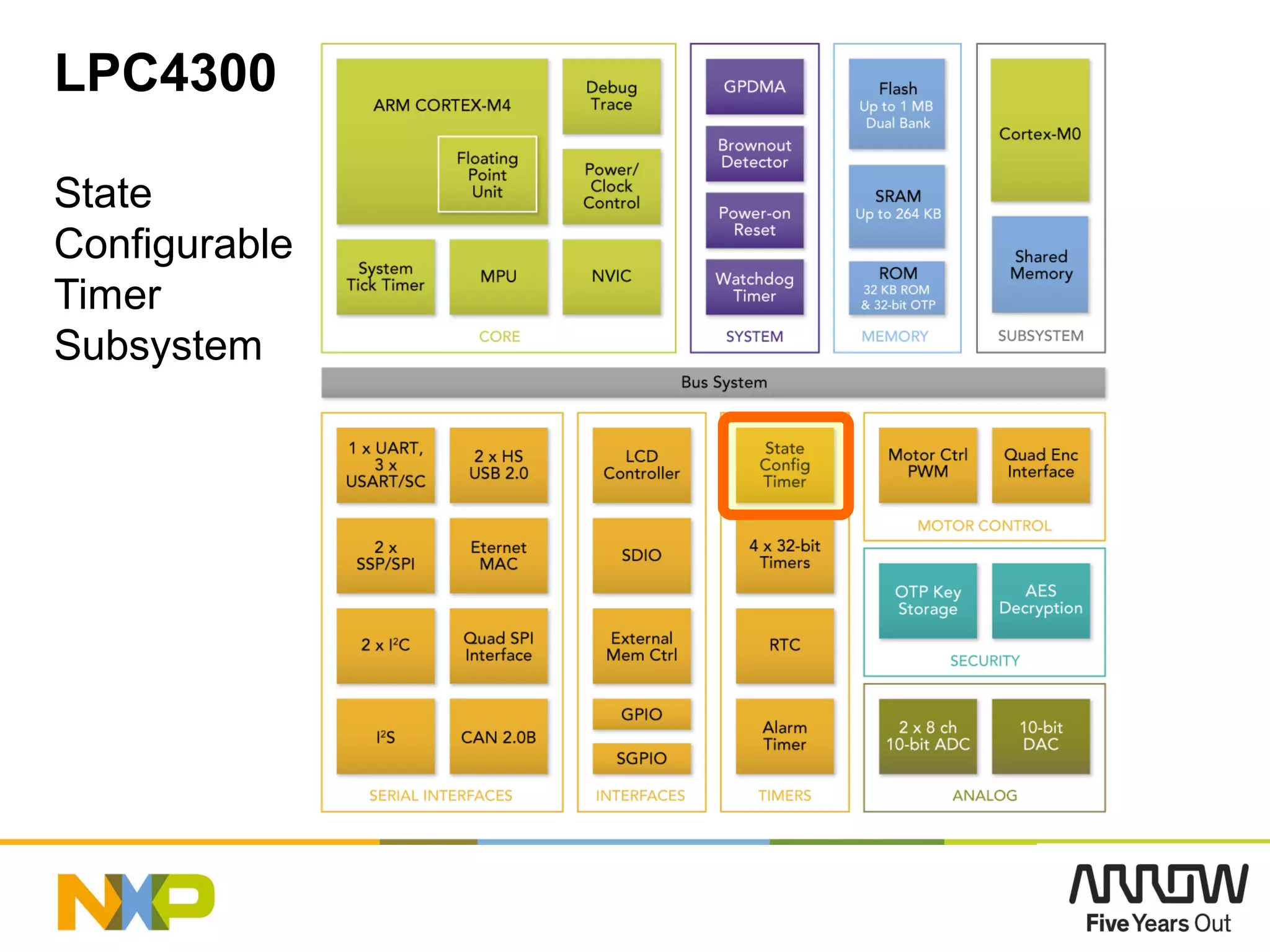
LPC4300 Block Diagram
LPC4300 Dual Core Microcontroller
13
Dual Core Microcontroller
Cortex M4 with FPU
Cortex M0
Asymetric implementation of the
two cores
Both cores are bus masters
Both cores can run on 204 MHz
Low leakage 90nm silicon
process
Flashless and on-chip flash
versions (external bus available
in all versions)
LPC4300 Part Numbers
Part# FlashTot Flash 1 Flash 2 SRAM LCD Ethnt HS USB CAN MaxFreq Package
LPC4357 1 MB 512 KB 512 KB 136 KB Y Y 2 2 204 LQFP208, BGA256/180
LPC4353 512 KB 256 KB 256 KB 136 KB Y Y 2 2 204 LQFP208, BGA256/180
LPC4350 0 KB 0 KB 0 KB 264KB Y Y 2 2 204 LQFP208, BGA256/180
LPC4337 1 MB 512 KB 512 KB 136 KB Y 2 2 204 LQFP208/144,
BGA256/180/100
LPC4333 512 KB 256 KB 256 KB 136 KB Y 2 2 204 LQFP208/144,
BGA256/180/100
LPC4330 0 KB 0 KB 0 KB 264KB Y 2 2 204 LQFP208/144,
BGA256/180/100
LPC4327 1 MB 512 KB 512 KB 136 KB 1 2 204 LQFP144/100, BGA100
LPC4325 768 KB 384 KB 384 KB 136 KB 1 2 204 LQFP144/100, BGA100
LPC4323 512 KB 256 KB 256 KB 104 KB 1 2 204 LQFP144/100, BGA100
LPC4322 512 KB 512 KB 0 KB 104 KB 1 2 204 LQFP144/100, BGA100
LPC4320 0 KB 0 KB 0 KB 200 KB 1 2 204 LQFP144/100, BGA100
LPC4317 1 MB 512 KB 512 KB 136 KB 2 204 LQFP144/100, BGA100
LPC4315 768 KB 384 KB 384 KB 136 KB 2 204 LQFP144/100, BGA100
LPC4313 512 KB 256 KB 256 KB 104 KB 2 204 LQFP144/100, BGA100
LPC4312 512 KB 512 KB 0 KB 104KB 2 204 LQFP144/100, BGA100
LPC4310 0 KB 0 KB 0 KB 168 KB 2 204 LQFP144/100, BGA100
LPC4300
ARM Cortex-M0
“The micro within”
Core: ARM Cortex-M0 Processor
32-bit ARM RISC processor
– Thumb 16-bit instruction set
+ some Thumb2 32-bit instruction
– 32-bit registers and operations
(e.g.single-cycle 32x32 multiply)
– Von Neumann architecture
Very power and area optimized
– Designed for low cost and low power silicon implementations
Automatic state saving on interrupts and exceptions
– Low software overhead on exception entry and exit
Deterministic instruction execution timing
– Interrupt latency of 16 cycles
16
LPC43xx Asymmetric Dual Core
Symmetric Asymmetric
Single application distributed over N
processors of the same type.
Each processor runs a different
application.
Requires OS support Specialized OS not required
Shared program memory Separate program resource per core
Dual Core: Symmetric vs Asymmetric
18
Core 1
Cache
Core 2
Cache
Program Memory
Core 1
Core 2
Program Memory Program Memory
Dual Core: Concept Overview
Cortex-M0 subsystem features
– Connection to the internal bus matrix giving access to all peripherals.
– NVIC for dedicated interrupt support of the opposite core
– Separate power control registers
– Shared memory for easy inter-processor communication (IPC)
– Tiny API implementation in ROM for IPC
PeripheralsPeripherals
AHB MatrixAHB Matrix
Cortex-M4Cortex-M4 Cortex-M0Cortex-M0Messaging
Queue
Messaging
Queue
19
Dual Core: LPC4300 boot sequence
20
Boot from
ROM
Boot from
ROMHeld in resetHeld in reset Step 1: M4 runs ROM bootloader
Held in resetHeld in reset Run from
flash
Run from
flash
Step 2: M4 runs application from flash
Setup M0Setup M0Held in resetHeld in reset
Release M0
from reset
Release M0
from reset
Run
Application
Run
Application
Step 3: M4 configures the M0
Step 4: M4 starts M0
Run
Application
Run
Application
Step 5: M4 runs application
M4M0
M4 and M0 can execute from
FLASH without contention
M0 can execute from its own
RAM area
ROM code written in Thumb
mode, which means that both
M4 and M0 can use ROM
code
M4 MPU can be used to
protect M0 code space
Dual Core: Memory Model
21
Dual Core: Bus Matrix ConnectionsAHBMatrix
CORTEX-M4
204MHz
CORTEX-M4
204MHz CORTEX-M0
204MHz
CORTEX-M0
204MHz
SRAM
128 KB
SRAM
128 KB
ROMROM
S I D
72 KB72 KB
External
Memory Ctrl
External
Memory Ctrl
32 KB32 KB
16 KB + 16 KB16 KB + 16 KB
Maximum performance is obtained when the code for each
processor is located in different memories.
• Cortex-M4 1.25 DMIPS/MHz
• Cortex-M0 0.9 DMIPS/MHz
Both Cortex-M4 & Cortex-M0 can run at 204MHz
22
Cortex-M4 works as number
cruncher, Cortex-M0 is
doing the house keeping
– Audio processing
– Motor control
Cortex-M4 runs RTOS and
application, Cortex-M0 is
doing time-critical and/or
stupid but time-consuming
jobs
– Industrial control
– Data router
Dual Core: Usage scenario examples
23
LPC4300
Cortex-M4Cortex-M4 Cortex-M0Cortex-M0
Data
I/O
LPC4300
Cortex-M0Cortex-M0 Cortex-M4Cortex-M4
Data
I/O
Real Time I/O
LPC4300
Dual Core: Audio application example
Cortex-M4: Full power devoted to Audio processing
Cortex-M0: Handles the hardware control – I2
S & USB
Cortex-M4Cortex-M4 Cortex-M0Cortex-M0
I2
S
USB
24
Dual Core: Audio processing data pathsAHBMatrix
CORTEX-M4
204MHz
CORTEX-M4
204MHz CORTEX-M0
204MHz
CORTEX-M0
204MHz
GPDMAGPDMA
SRAM
128 KB
SRAM
128 KB
ROMROM
S I D
72 KB72 KB
Ether
net
Ether
net
USB0USB0 USB1USB1
HS PHYHS PHY FS PHY
+ ULPI
FS PHY
+ ULPI
External
Memory Ctrl
External
Memory Ctrl
LCDLCDSD/
MMC
SD/
MMC
0 1
32 KB32 KB
16 KB + 16 KB16 KB + 16 KB
AHB
Peripherals
AHB
Peripherals
APB
Peripherals
APB
Peripherals
25
Dual Core: Motor control example
LPC4300
Cortex-M4Cortex-M4 Cortex-M0Cortex-M0
Cortex-M4: Single shunt Field Oriented Control (FOC)
Cortex-M0: Receives control commands via CAN interface
SCTSCT CANCAN Command
26
Dual Core: Motor control data pathsAHBMatrix
CORTEX-M4
204MHz
CORTEX-M4
204MHz CORTEX-M0
204MHz
CORTEX-M0
204MHz
GPDMAGPDMA
SRAM
128 KB
SRAM
128 KB
ROMROM
S I D
72 KB72 KB
Ether
net
Ether
net
USB0USB0 USB1USB1
HS PHYHS PHY FS PHY
+ ULPI
FS PHY
+ ULPI
External
Memory Ctrl
External
Memory Ctrl
LCDLCDSD/
MMC
SD/
MMC
0 1
32 KB32 KB
16 KB + 16 KB16 KB + 16 KB
AHB
Peripherals
AHB
Peripherals
APB
Peripherals
APB
Peripherals
27
Cortex-M0 Subsystem - Development
Takes advantages of the best features of the latest development tools:
Cortex-M4 and Cortex-M0 share a debug interface allowing a single
JTAG/SWD unit to debug both cores
28
Advance
Inform
ation
LPC4300
SPI Flash
Interface
Advance
Inform
ation
29
Microcontroller Flash
There are 3 main types of MCU Flash typically used:
1. On-chip Flash
– Advantages: Fastest, secure, single chip solution
– Disadvantages: Most expensive
2. Parallel Flash
– Advantages: Fast
– Disadvantages: Large package/many pins, Expensive
3. Serial (SPI) Flash
– Advantages: Small package/few pins, least expensive
– Disadvantages: Slow and Complicated
SPIFI balances speed & cost
SPI Flash Interface
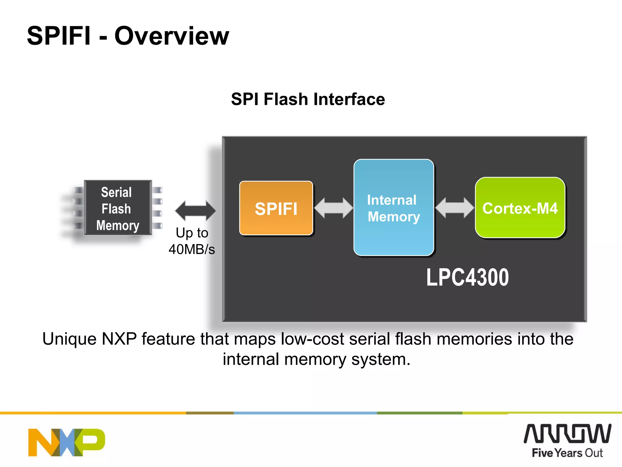
Unique NXP feature that maps low-cost serial flash memories into the
internal memory system.
LPC4300
SPIFI - Overview
31
Advance
Inform
ation
Internal
Memory
Internal
Memory Cortex-M4Cortex-M4SPIFISPIFI
Serial
Flash
Memory
Up to
40MB/s
SPIFI – Image Storage – Problem
• Devices with complex user
interfaces require storage
for images that will be
displayed on an LCD.
• Images can be stored in
external SPI flash but
usually have to be copied
into RAM and then sent to
LCD controller.
• Problem with this approach
is that it uses large
amounts of RAM
34
Microcontroller
Flash
Memory
Flash
Memory
RAMRAM
CPU
Core
CPU
Core
LCD
Controller
LCD
Controller
SPIFI – Image Storage – Solution
• Image stored within external
serial flash memory
• High speed quad SPI interface
allows images to be
transferred directly to LCD
controller using DMA
• Advantages of a SPIFI based
solution:
• Does not use precious
internal SRAM or require
external SDRAM for image
frame buffers.
35
LPC4300
LCD
Controller
LCD
ControllerSPIFISPIFI
Serial
Flash
Memory
LPC4300
State
Configurable
Timer
Subsystem
Advance
Inform
ation
36
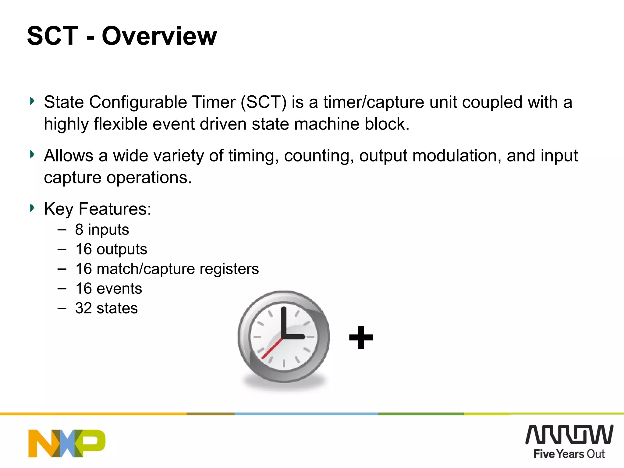
SCT - Overview
State Configurable Timer (SCT) is a timer/capture unit coupled with a
highly flexible event driven state machine block.
Allows a wide variety of timing, counting, output modulation, and input
capture operations.
Key Features:
– 8 inputs
– 16 outputs
– 16 match/capture registers
– 16 events
– 32 states
37
+
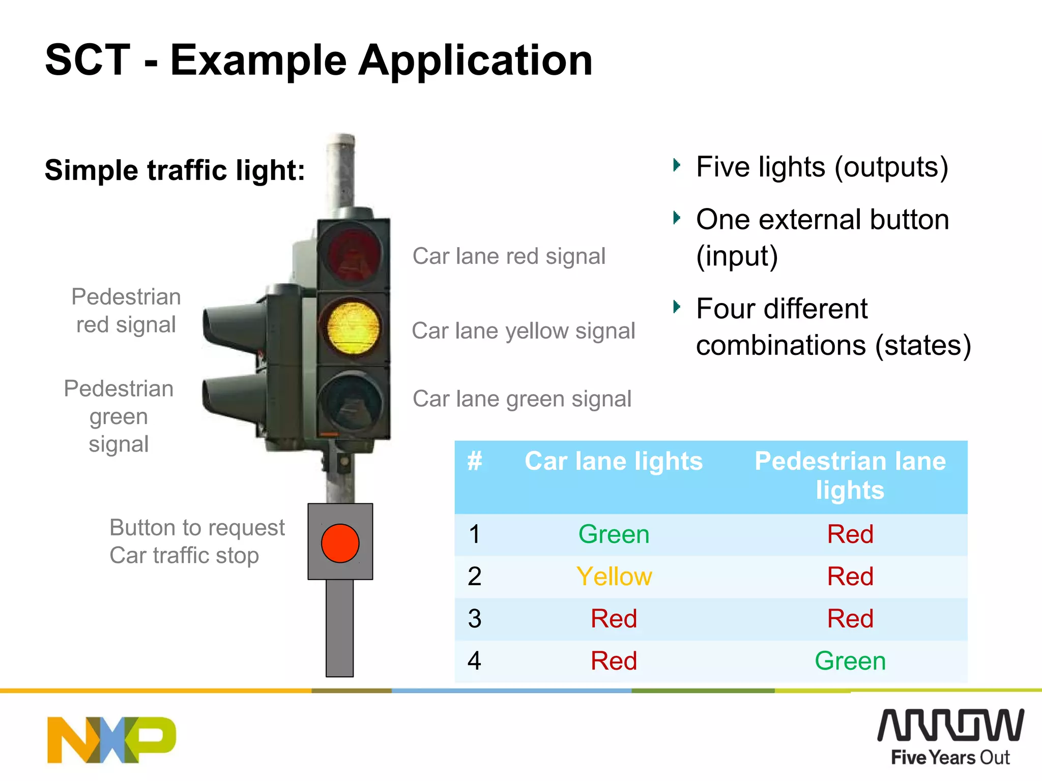
SCT - Example Application
38
Pedestrian
red signal
Pedestrian
green
signal
Car lane red signal
Car lane yellow signal
Car lane green signal
Button to request
Car traffic stop
# Car lane lights Pedestrian lane
lights
1 Green Red
2 Yellow Red
3 Red Red
4 Red Green
Five lights (outputs)
One external button
(input)
Four different
combinations (states)
Simple traffic light:
SCT – Easy to use
39
1. Design the state machine
LPC_SCT->CTRL |= (1UL << 7);
LPC_SCT->TIM = 0x4534;
LPC_SCT->ENB &= 0x8001;
2. Set the registers/timer
3. Let the SCT do the work!
Library of examples
will be available!
SCT allows this application to be implemented in hardware!
LPC4300
Serial
GPIO
40
SGPIO - Overview
Serial GPIO (SGPIO) = GPIO + Timer/Shift Register:
– Used to create or captures multiple real time serial data streams.
– No more having to write code loops to manipulate GPIO in real time.
– Easily replaces CPU intensive ‘bit banging’
Key Features:
– Up to 16 inputs/outputs each with their own timer/shift register unit.
– Counter to control the rate at which data is clocked in/out.
– Counter to control the number of bits clocked out/in.
– Output has three states high, low, or high impedance.
41
Advance
Inform
ation
SGPIOSGPIOCPU
Core
CPU
Core
SGPIO can be used to emulate proprietary serial interfaces
Configure SGPIO to generate desired waveform(s) with just a few register writes.
LPC4300
USB 2.0
Ethernet
42
Interfaces – USB & Ethernet
Two USB 2.0 Interfaces:
– USB 2.0 Host/Device/OTG interfaces.
– One with on-chip high-speed PHY.
– One with on-chip full-speed PHY and ULPI interface for external high
speed PHY
– FREE nxpUSBlib Driver Library!
Ethernet MAC with RMII and MII interfaces to external transceiver:
– Supports 10/100 Mbit/s
– TCP/IP hardware checksum
– DMA support allows high throughput at low CPU load
– IEEE 1588 advanced time stamp support.
– FREE LWIP TCP/IP Stack!
43
LPC4300
LCD
Controller
44
LCD Controller (on LPC435x types only)
– Resolution up to 1024 x 768 pixels
– Support for Thin Film Transistor (TFT) color displays, from
monochrome through palettized or up to 24 bpp direct true-color
– Single and dual panel STN color displays
– Hardware Cursor support for single panel displays
– Dedicated DMA and display buffer FIFO improve performance
– Touchscreens can be supported by using standard GPIO ports and
two ADC channels
LCD Controller
45
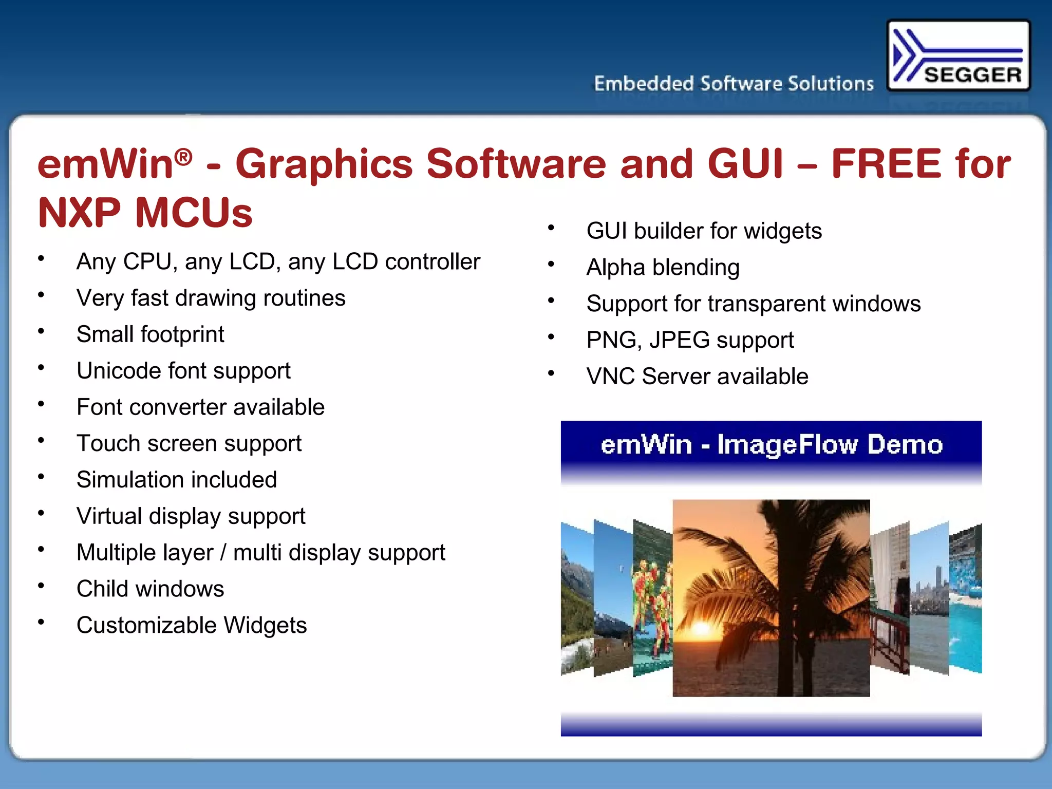
emWin®
- Graphics Software and GUI – FREE for
NXP MCUs
• Any CPU, any LCD, any LCD controller
• Very fast drawing routines
• Small footprint
• Unicode font support
• Font converter available
• Touch screen support
• Simulation included
• Virtual display support
• Multiple layer / multi display support
• Child windows
• Customizable Widgets
• GUI builder for widgets
• Alpha blending
• Support for transparent windows
• PNG, JPEG support
• VNC Server available
LPC4300 Ecosystem and software
48
49
50
WWW.LPC4350.COM
Cortex-M4 and M0 projects
need to be set up as seperate
projects in an IDE like µVision
Output of the M0 project can
be embedded as input source
for the M4 project
Source files like LPC4300
register definitions or config
files can be shared
Dual Core: Software development
*
Cortex-M4 and Cortex-M0
share single JTAG unit to
debug both cores
Cortex-M4 provides SWD
and ETM
Dual core debugging
supported by major tool
providers
1.IAR
2.KEIL
3.Code Red
4.PLS
5.etc
Dual Core: Software debugging
*
Core: FPU support in the toolchains
GNU Compiler
1.Code Sourcery Lite: newlib does not support the direct use of the FPU
registers. Cortex-M4 registers r0-r3 and stack is used instead.
1.Options: --march=armv7e-m --mthumb --mfloat-abi=softfp --mfpu=fpv4-sp-d16
2.Code Sourcery G++: comes with libraries supporting direct use of FPU
registers
1.Options: --march=armv7e-m --mthumb --mfloat-abi=hard --mfpu=fpv4-sp-d16
3.Code Red: Red Suite comes with libraries for direct FPU support
ARM/KEIL: full support for FPU
1.Option: --cpu Cortex-M4.fp
IAR: full support for FPU
1.Option: --fpu=VFPv4_sp
*
LPC18xx/43xx pin muxing tool
Java tool
Helps hardware designer with pin multiplexing
Generates source code for pin mux control
*
COMPANY CONFIDENTIAL
Training, videos, books, source codes & demos and much more
www.lpcware.com
www.lpc4350.com
www.nxp.com
COMPANY CONFIDENTIAL
Only
In
Arrow
COMPANY CONFIDENTIAL

Arrow multisolution nxp lpc4300 dual core

  • 1.
    LPC4300 Cortex-M4 +M0Dual Core Microcontrollers Arrow Israel Amir Sherman Semiconductors Technical Manager
  • 2.
    NXP is aleader in ARM Flash MCUs Clear strategy: 100% focus on ARM Top performance through leading technology & architecture Design flexibility through pin- and software-compatible solutions – Scalable memory sizes – Widest range of peripherals Unlimited choice through complete families for multiple cores Cortex M4 Cortex M3 Cortex M0 ARM7 ARM9 8051
  • 3.
    32-bit16-bit8-bit NXP Changing MicrocontrollerLandscape DSP cost performance Very low-end 8b e.g. 6-8 pin not planned High-end DSP/MPU not planned ARM Cortex-M Continuum Cortex-M4Cortex-M3Cortex-M0 Breaking through traditional boundaries of 8b, 16b, 32b and DSP The ONLY vendor that offers the full range of ARM Cortex-M microcontroller families Binary and tool compatible
  • 4.
  • 5.
    COMPANY CONFIDENTIAL Cortex-M0 Up to50MHz Cortex-M0 Up to 50MHz Cortex-M3 Up to 180MHz Cortex-M3 Up to 180MHz Cortex-M4 Up to 204MHz Cortex-M4 Up to 204MHz Rapidly growing family of Cortex-M microcontrollers  For more information: www.nxp.com/microcontrollers 5 LPC1100LPC1100 LPC1200LPC1200 LPC1300LPC1300 LPC1700LPC1700 LPC1800LPC1800 LPC4300LPC4300 Best-in-class dynamic power consumption Memory options up to 128k flash USB solution, incl. on-chip USB drivers High-performance with USB, Ethernet, LCD, and more Memory options up to 1MB flash, 200k SRAM High performance M4/M0 DSC with advanced peripherals LPC40xxLPC40xx High-performance M4 with USB, Ethernet, LCD, and more 5
  • 6.
    Company Confidential LPC1800 -180MHz M3, HSUSB,advanced peripherals LPC1700 - M3 family with USB, Ethernet and LCD LPC1300 - Lowest Power Cortex M3 with USB M4 (Up to 204MHz) LPC4300 M3 (Up to 120MHz) LPC1700 NXP Mid/High-End Portfolio At A Glance 6 ARM7 (Up to 72MHz) LH7xxxx, LPC2400, LPC2300, LPC2200, LPC2100 ClockSpeed Memory Size LH7xxxx - LCD Graphics microcontroller LPC2400 – Adds LCD-controller and External Memory Interface LPC2300 – Dual AHB Bus MCUs with USB and Ethernet LPC2200 – Adds External Memory Interface LPC2100 – Low cost ARM7 microcontrollers LPC2300/2400 – LPC1700 LPC1800 – LPC4300 M3 (Up to 180MHz) LPC1800 M4 (Up to 120MHz) LPC4000
  • 7.
    Company Confidential Cortex-M4Cortex-M4 NXP Cortex-M4offerings Flash LCD, Eth, 2 HS USB, FPU, EMC Ethernet, 2 HS USB, FPU, EMC +2 comp, FPU, LCD LPC4312LPC4312LPC4310LPC4310 LPC4320LPC4320 LPC4330LPC4330 LPC4350LPC4350 LPC4313LPC4313 LPC4323LPC4323 LPC4333LPC4333 LPC4353LPC4353 LPC4322LPC4322 0 KB 128 KB 256 KB 512 KB 768 KB 1 MB LPC4317LPC4317 LPC4337LPC4337 LPC4357LPC4357 LPC4327LPC4327 LPC4315LPC4315 LPC4325LPC4325 LPC4088LPC4088 LPC4078LPC4078 LPC4076LPC4076 LPC4074LPC4074 1 USB, FPU, EMC +2 comp, FPU Performance/Features 204MHz120MHz No FPU or comp +2 comp, FPU LPC43S50LPC43S50 LPC43A50LPC43A50
  • 8.
    Company Confidential • LPC40xxCortex-M4 parts are pin-compatible with the popular NXP LPC1700 Cortex-M3 and ARM7 MCUs to easily allow customer project migration – LPC408x is pin-compatible to the LPC178x and LPC247x series – LPC407x is pin-compatible to the LPC177x and LPC246x, LPC245x and LPC238x series Bridging ARM7 to Cortex-M3 to Cortex-M4 8
  • 9.
    Company Confidential • Cortex-M432-bit DSC • Single cycle MAC • SIMD instructions • Memory Protection Unit • Floating Point Unit (most parts) • CRC Calculation engine • Up to 120 MHz performance • Memories • Up to 512 KB Flash memory (zero wait state) • Up to 96 KB SRAM (3 blocks) • Up to 4 KB EEPROM • Serial Peripherals: • SPI Flash Interface • 10/100 Ethernet MAC • USB 2.0 full-speed device/host/OTG • Four UARTs + one USART • Two CAN 2.0B controllers • Three SSP/SPI controllers • Three I2C (one with FM+) • SD/MMC • I2S interface • Analog Peripherals • 12-bit ADC with 8 channels (400 KSPS) • 10-bit digital-to-analog converter • Two analog comparators (most parts) • Other Peripherals • Up to 32-bit External Memory Controller • Low Power Real-time clock • 3-input Event Recorder • Eight-channel, general-purpose DMA • Up to 165 GPIO • Motor control PWM • Quadrature encoder interface • Four 32-bit timers/counters • 12 MHz internal RC oscillator trimmed to 1% accuracy • ARM Ecosystem • Write in C for a 32-bit processor • ROM drivers / free software libraries • Pin- and software-compatible with the LPC177x/8x series Introducing the LPC40xx Family
  • 10.
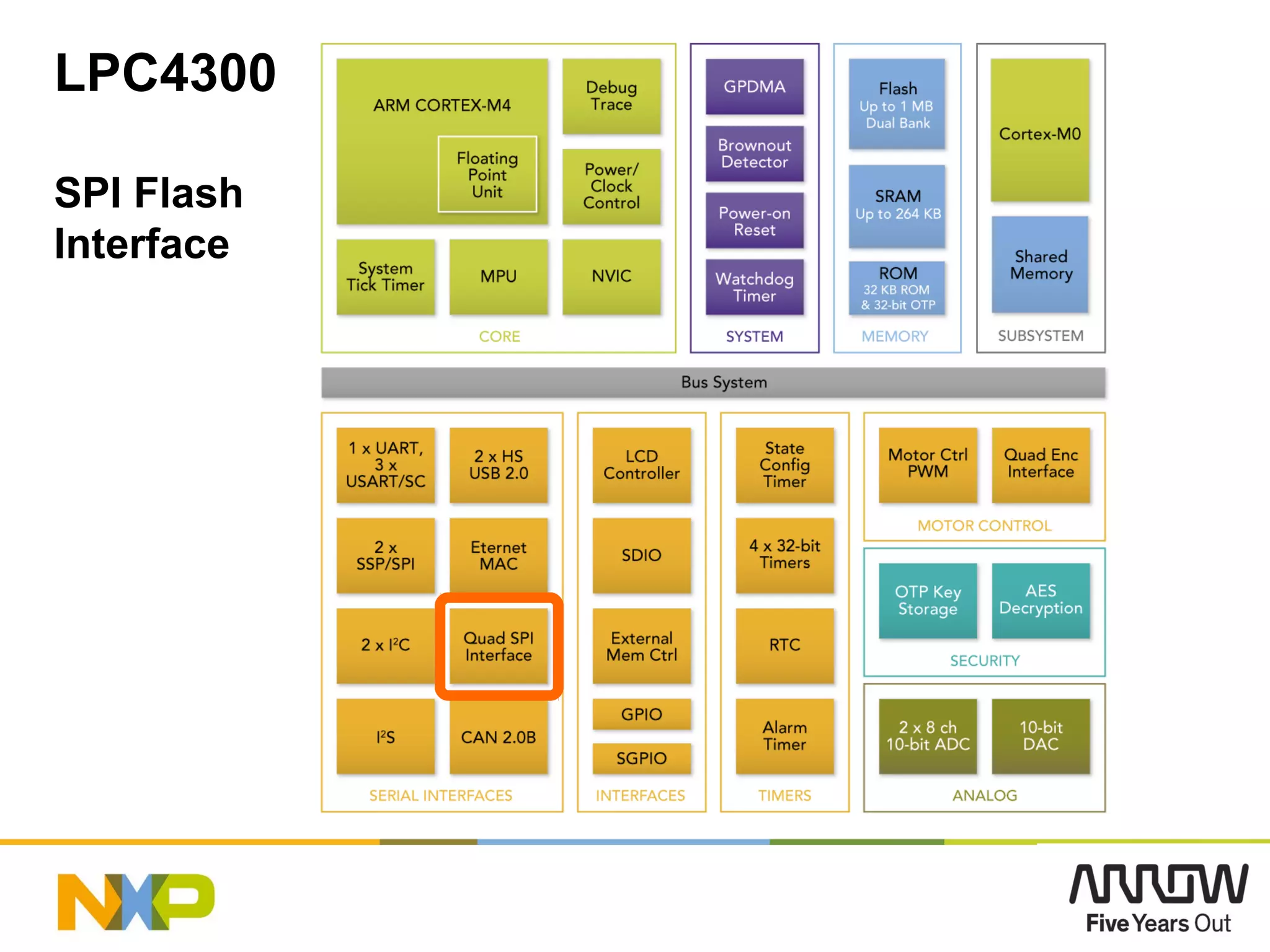
    Company Confidential 10 LPC408x/7x BlockDiagram INTERFACES TIMERS MOTOR CONTROL 4 x 32 bit Timers 4 x 32 bit Timers RTC w/ Event Recorder RTC w/ Event Recorder Tick TimerTick Timer Standard PWM Standard PWM ANALOG 12-Bit / 8 Ch ADC 12-Bit / 8 Ch ADC 10-Bit DAC 10-Bit DAC SYSTEM GPDMAGPDMA Brownout Detector Brownout Detector Power-On Reset Power-On Reset Watchdog Timer Watchdog Timer MEMORY Flash 128KB – 512KB Flash 128KB – 512KB SRAM 40KB to 96KB SRAM 40KB to 96KB ROMROM CORE ARM CORTEX- M4 Up to 120MHz ARM CORTEX- M4 Up to 120MHz MPUMPU NVICNVIC WICWIC Debug Trace Debug Trace Bus System CPU PLLCPU PLL USB PLLUSB PLL CRC Engine CRC Engine IRCIRC 5 x UART5 x UART 3 x SSP/SPI 3 x SSP/SPI 2 x I2 C2 x I2 C I2 C FM+I2 C FM+ FS USB 2.0 H/D/O FS USB 2.0 H/D/O Ethernet MAC Ethernet MAC External Mem Ctrl External Mem Ctrl 2x CAN 2.0B 2x CAN 2.0B SD/MMCSD/MMC Quad Enc Interface Quad Enc Interface Motor Ctrl PWM Motor Ctrl PWM 2 x I2 S2 x I2 S EEPROM 2KB – 4KB EEPROM 2KB – 4KB 2x Comparator 2x ComparatorGraphic LCD Graphic LCD FPUFPU SPI Flash Interface SPI Flash Interface Cortex-M4 performance @ 120MHz Full LCD Graphics controller Unique SPI Flash Interface memory maps low cost external Quad SPI Flash. Can execute code via SPIFI! NXP Unique Up to 32-bit full external Memory Interface NXP Unique Up to 512 KB on chip flash memory New NXP USART with support for Smart Card Interface New NXP Event Recorder in RTC domain for Anti- Tampering protection Two analog comparators
  • 11.
    Company Confidential LPC40xx Schedule& Part Numbers Product Flash Total SRAM EEPROM Ext Bus LCD Enet UART USB CAN I2S QEI SD DAC SPIFI Comp FPU Package LPC4088 512KB 96KB 4KB 32 Y Y 5 H/O/D 2 Y Y Y Y Y Y Y LQFP208, TFBGA208, TFBGA180, LQFP144 LPC4078 512KB 96KB 4KB 32 N Y 5 H/O/D 2 Y Y Y Y Y Y Y LQFP208, TFBGA180, LQFP80 LPC4076 256KB 80KB 4KB 32 N Y 5 H/O/D 2 Y Y Y Y Y N N TFBGA180 LPC4074 128KB 40KB 2KB 32 N N 5 D 2 Y N N Y Y N N LQFP144, LQFP80 11
  • 12.
    Company Confidential • Cortex-M432-bit DSC • Single cycle MAC • SIMD instructions • Floating Point Unit Cortex-M0 32-bit coprocessor Up to 204 MHz performance Up to 1 MB Flash • Dual-Bank Flash provides safe in- application programming (IAP) • Large SRAM: up to 264 kB SRAM • SPI Flash Interface with four lanes and up to 60MB/s data transfer rate. • State Configurable Timer Subsystem • Serial GPIO (SGPIO) • Extensive connectivity including: • Two High-speed USB 2.0 interfaces w/ an on-chip High-speed PHY • 120 MHz External Memory Interface with 8 Chip Selects • 10/100 Ethernet MAC • LCD controller (Up to 1024H × 768V) • SDIO interface • 4x UARTs, 2x I2C, 2x I2S, 2x CAN 2.0B, 3x SSP/SPI • 2x 10-bit 400ksps ADCs and 10-bit DAC • Motor Control PWM • Quadrature Encoder Interface • Up to 164 general purpose I/O pins • ARM Ecosystem • Write in C for a 32-bit processor • Code compatible dual-cores • One debugger for dual-core • ROM drivers / free software libraries • Pin- and software-compatible with the LPC1800 series Introducing the LPC4300 Family
  • 13.
    LPC4300 Block Diagram LPC4300Dual Core Microcontroller 13 Dual Core Microcontroller Cortex M4 with FPU Cortex M0 Asymetric implementation of the two cores Both cores are bus masters Both cores can run on 204 MHz Low leakage 90nm silicon process Flashless and on-chip flash versions (external bus available in all versions)
  • 14.
    LPC4300 Part Numbers Part#FlashTot Flash 1 Flash 2 SRAM LCD Ethnt HS USB CAN MaxFreq Package LPC4357 1 MB 512 KB 512 KB 136 KB Y Y 2 2 204 LQFP208, BGA256/180 LPC4353 512 KB 256 KB 256 KB 136 KB Y Y 2 2 204 LQFP208, BGA256/180 LPC4350 0 KB 0 KB 0 KB 264KB Y Y 2 2 204 LQFP208, BGA256/180 LPC4337 1 MB 512 KB 512 KB 136 KB Y 2 2 204 LQFP208/144, BGA256/180/100 LPC4333 512 KB 256 KB 256 KB 136 KB Y 2 2 204 LQFP208/144, BGA256/180/100 LPC4330 0 KB 0 KB 0 KB 264KB Y 2 2 204 LQFP208/144, BGA256/180/100 LPC4327 1 MB 512 KB 512 KB 136 KB 1 2 204 LQFP144/100, BGA100 LPC4325 768 KB 384 KB 384 KB 136 KB 1 2 204 LQFP144/100, BGA100 LPC4323 512 KB 256 KB 256 KB 104 KB 1 2 204 LQFP144/100, BGA100 LPC4322 512 KB 512 KB 0 KB 104 KB 1 2 204 LQFP144/100, BGA100 LPC4320 0 KB 0 KB 0 KB 200 KB 1 2 204 LQFP144/100, BGA100 LPC4317 1 MB 512 KB 512 KB 136 KB 2 204 LQFP144/100, BGA100 LPC4315 768 KB 384 KB 384 KB 136 KB 2 204 LQFP144/100, BGA100 LPC4313 512 KB 256 KB 256 KB 104 KB 2 204 LQFP144/100, BGA100 LPC4312 512 KB 512 KB 0 KB 104KB 2 204 LQFP144/100, BGA100 LPC4310 0 KB 0 KB 0 KB 168 KB 2 204 LQFP144/100, BGA100 LPC4300
  • 15.
  • 16.
    Core: ARM Cortex-M0Processor 32-bit ARM RISC processor – Thumb 16-bit instruction set + some Thumb2 32-bit instruction – 32-bit registers and operations (e.g.single-cycle 32x32 multiply) – Von Neumann architecture Very power and area optimized – Designed for low cost and low power silicon implementations Automatic state saving on interrupts and exceptions – Low software overhead on exception entry and exit Deterministic instruction execution timing – Interrupt latency of 16 cycles 16
  • 17.
  • 18.
    Symmetric Asymmetric Single applicationdistributed over N processors of the same type. Each processor runs a different application. Requires OS support Specialized OS not required Shared program memory Separate program resource per core Dual Core: Symmetric vs Asymmetric 18 Core 1 Cache Core 2 Cache Program Memory Core 1 Core 2 Program Memory Program Memory
  • 19.
    Dual Core: ConceptOverview Cortex-M0 subsystem features – Connection to the internal bus matrix giving access to all peripherals. – NVIC for dedicated interrupt support of the opposite core – Separate power control registers – Shared memory for easy inter-processor communication (IPC) – Tiny API implementation in ROM for IPC PeripheralsPeripherals AHB MatrixAHB Matrix Cortex-M4Cortex-M4 Cortex-M0Cortex-M0Messaging Queue Messaging Queue 19
  • 20.
    Dual Core: LPC4300boot sequence 20 Boot from ROM Boot from ROMHeld in resetHeld in reset Step 1: M4 runs ROM bootloader Held in resetHeld in reset Run from flash Run from flash Step 2: M4 runs application from flash Setup M0Setup M0Held in resetHeld in reset Release M0 from reset Release M0 from reset Run Application Run Application Step 3: M4 configures the M0 Step 4: M4 starts M0 Run Application Run Application Step 5: M4 runs application M4M0
  • 21.
    M4 and M0can execute from FLASH without contention M0 can execute from its own RAM area ROM code written in Thumb mode, which means that both M4 and M0 can use ROM code M4 MPU can be used to protect M0 code space Dual Core: Memory Model 21
  • 22.
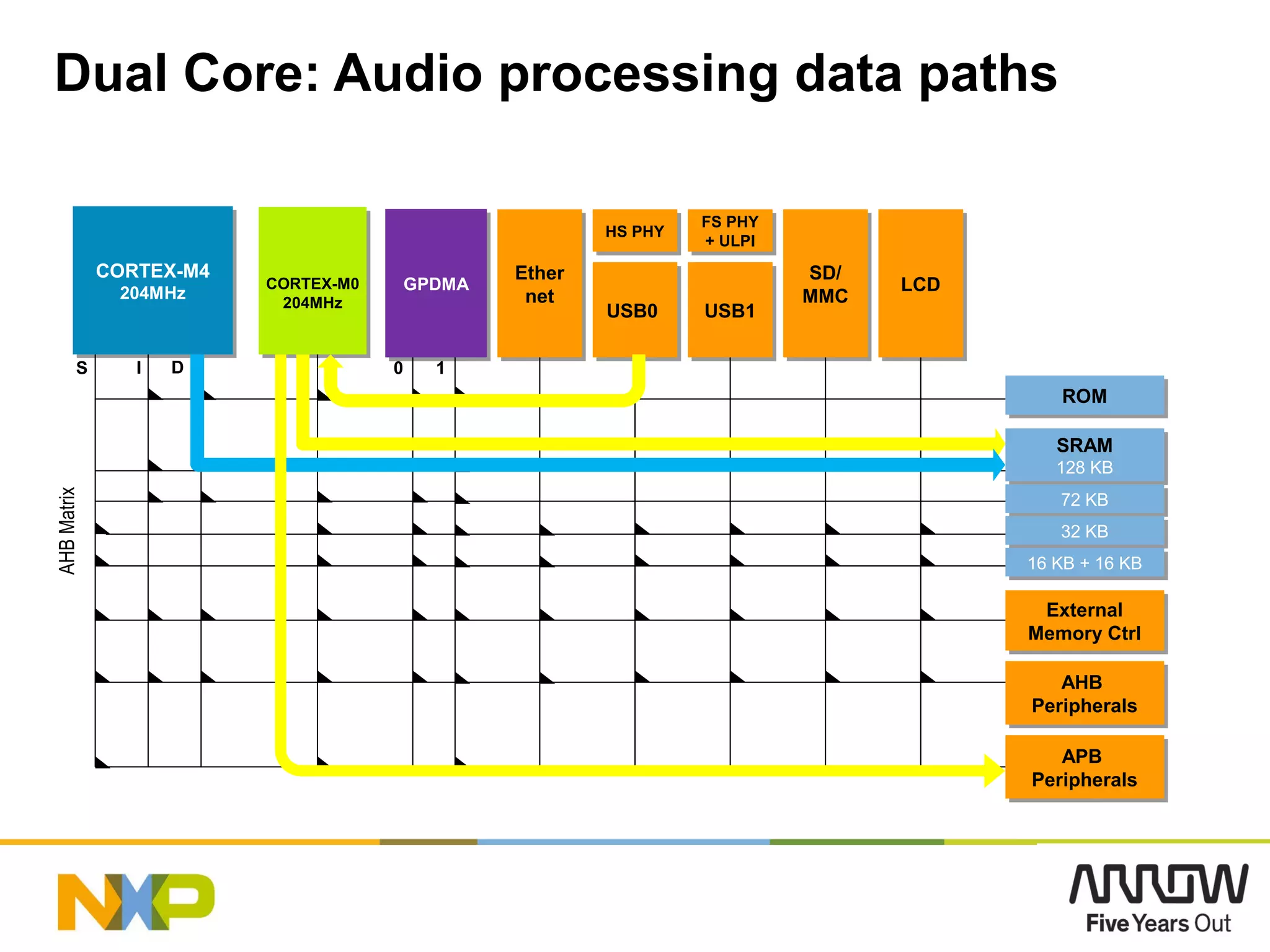
    Dual Core: BusMatrix ConnectionsAHBMatrix CORTEX-M4 204MHz CORTEX-M4 204MHz CORTEX-M0 204MHz CORTEX-M0 204MHz SRAM 128 KB SRAM 128 KB ROMROM S I D 72 KB72 KB External Memory Ctrl External Memory Ctrl 32 KB32 KB 16 KB + 16 KB16 KB + 16 KB Maximum performance is obtained when the code for each processor is located in different memories. • Cortex-M4 1.25 DMIPS/MHz • Cortex-M0 0.9 DMIPS/MHz Both Cortex-M4 & Cortex-M0 can run at 204MHz 22
  • 23.
    Cortex-M4 works asnumber cruncher, Cortex-M0 is doing the house keeping – Audio processing – Motor control Cortex-M4 runs RTOS and application, Cortex-M0 is doing time-critical and/or stupid but time-consuming jobs – Industrial control – Data router Dual Core: Usage scenario examples 23 LPC4300 Cortex-M4Cortex-M4 Cortex-M0Cortex-M0 Data I/O LPC4300 Cortex-M0Cortex-M0 Cortex-M4Cortex-M4 Data I/O Real Time I/O
  • 24.
    LPC4300 Dual Core: Audioapplication example Cortex-M4: Full power devoted to Audio processing Cortex-M0: Handles the hardware control – I2 S & USB Cortex-M4Cortex-M4 Cortex-M0Cortex-M0 I2 S USB 24
  • 25.
    Dual Core: Audioprocessing data pathsAHBMatrix CORTEX-M4 204MHz CORTEX-M4 204MHz CORTEX-M0 204MHz CORTEX-M0 204MHz GPDMAGPDMA SRAM 128 KB SRAM 128 KB ROMROM S I D 72 KB72 KB Ether net Ether net USB0USB0 USB1USB1 HS PHYHS PHY FS PHY + ULPI FS PHY + ULPI External Memory Ctrl External Memory Ctrl LCDLCDSD/ MMC SD/ MMC 0 1 32 KB32 KB 16 KB + 16 KB16 KB + 16 KB AHB Peripherals AHB Peripherals APB Peripherals APB Peripherals 25
  • 26.
    Dual Core: Motorcontrol example LPC4300 Cortex-M4Cortex-M4 Cortex-M0Cortex-M0 Cortex-M4: Single shunt Field Oriented Control (FOC) Cortex-M0: Receives control commands via CAN interface SCTSCT CANCAN Command 26
  • 27.
    Dual Core: Motorcontrol data pathsAHBMatrix CORTEX-M4 204MHz CORTEX-M4 204MHz CORTEX-M0 204MHz CORTEX-M0 204MHz GPDMAGPDMA SRAM 128 KB SRAM 128 KB ROMROM S I D 72 KB72 KB Ether net Ether net USB0USB0 USB1USB1 HS PHYHS PHY FS PHY + ULPI FS PHY + ULPI External Memory Ctrl External Memory Ctrl LCDLCDSD/ MMC SD/ MMC 0 1 32 KB32 KB 16 KB + 16 KB16 KB + 16 KB AHB Peripherals AHB Peripherals APB Peripherals APB Peripherals 27
  • 28.
    Cortex-M0 Subsystem -Development Takes advantages of the best features of the latest development tools: Cortex-M4 and Cortex-M0 share a debug interface allowing a single JTAG/SWD unit to debug both cores 28 Advance Inform ation
  • 29.
  • 30.
    Microcontroller Flash There are3 main types of MCU Flash typically used: 1. On-chip Flash – Advantages: Fastest, secure, single chip solution – Disadvantages: Most expensive 2. Parallel Flash – Advantages: Fast – Disadvantages: Large package/many pins, Expensive 3. Serial (SPI) Flash – Advantages: Small package/few pins, least expensive – Disadvantages: Slow and Complicated SPIFI balances speed & cost
  • 31.
    SPI Flash Interface UniqueNXP feature that maps low-cost serial flash memories into the internal memory system. LPC4300 SPIFI - Overview 31 Advance Inform ation Internal Memory Internal Memory Cortex-M4Cortex-M4SPIFISPIFI Serial Flash Memory Up to 40MB/s
  • 32.
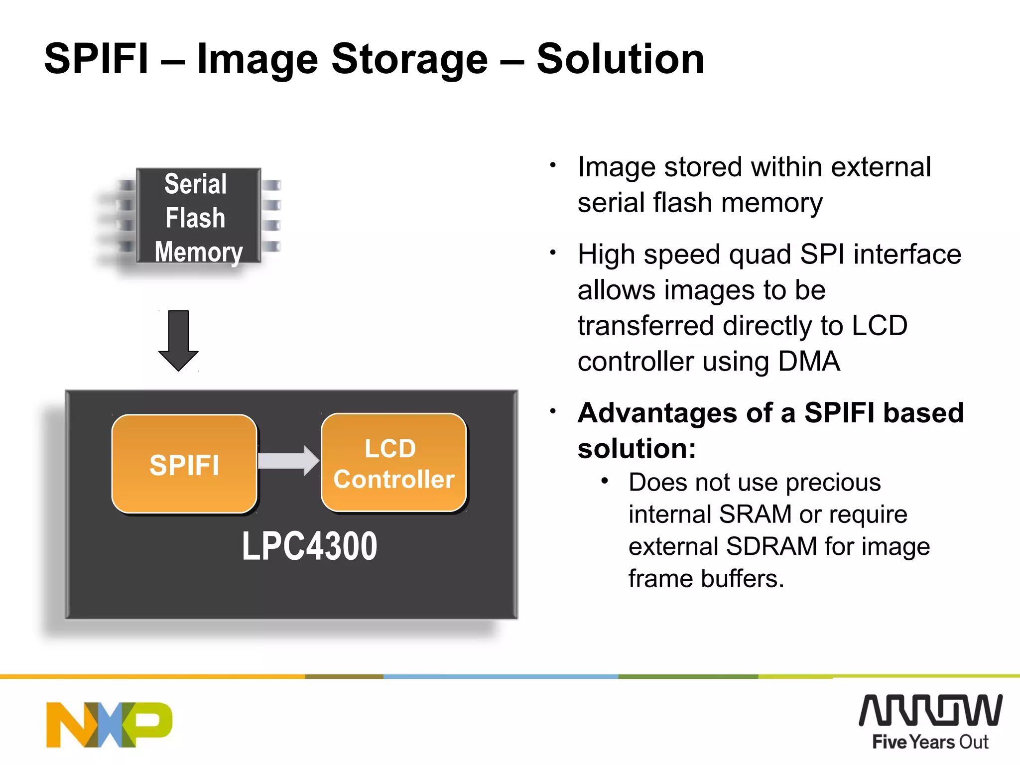
    SPIFI – ImageStorage – Problem • Devices with complex user interfaces require storage for images that will be displayed on an LCD. • Images can be stored in external SPI flash but usually have to be copied into RAM and then sent to LCD controller. • Problem with this approach is that it uses large amounts of RAM 34 Microcontroller Flash Memory Flash Memory RAMRAM CPU Core CPU Core LCD Controller LCD Controller
  • 33.
    SPIFI – ImageStorage – Solution • Image stored within external serial flash memory • High speed quad SPI interface allows images to be transferred directly to LCD controller using DMA • Advantages of a SPIFI based solution: • Does not use precious internal SRAM or require external SDRAM for image frame buffers. 35 LPC4300 LCD Controller LCD ControllerSPIFISPIFI Serial Flash Memory
  • 34.
  • 35.
    SCT - Overview StateConfigurable Timer (SCT) is a timer/capture unit coupled with a highly flexible event driven state machine block. Allows a wide variety of timing, counting, output modulation, and input capture operations. Key Features: – 8 inputs – 16 outputs – 16 match/capture registers – 16 events – 32 states 37 +
  • 36.
    SCT - ExampleApplication 38 Pedestrian red signal Pedestrian green signal Car lane red signal Car lane yellow signal Car lane green signal Button to request Car traffic stop # Car lane lights Pedestrian lane lights 1 Green Red 2 Yellow Red 3 Red Red 4 Red Green Five lights (outputs) One external button (input) Four different combinations (states) Simple traffic light:
  • 37.
    SCT – Easyto use 39 1. Design the state machine LPC_SCT->CTRL |= (1UL << 7); LPC_SCT->TIM = 0x4534; LPC_SCT->ENB &= 0x8001; 2. Set the registers/timer 3. Let the SCT do the work! Library of examples will be available! SCT allows this application to be implemented in hardware!
  • 38.
  • 39.
    SGPIO - Overview SerialGPIO (SGPIO) = GPIO + Timer/Shift Register: – Used to create or captures multiple real time serial data streams. – No more having to write code loops to manipulate GPIO in real time. – Easily replaces CPU intensive ‘bit banging’ Key Features: – Up to 16 inputs/outputs each with their own timer/shift register unit. – Counter to control the rate at which data is clocked in/out. – Counter to control the number of bits clocked out/in. – Output has three states high, low, or high impedance. 41 Advance Inform ation SGPIOSGPIOCPU Core CPU Core SGPIO can be used to emulate proprietary serial interfaces Configure SGPIO to generate desired waveform(s) with just a few register writes.
  • 40.
  • 41.
    Interfaces – USB& Ethernet Two USB 2.0 Interfaces: – USB 2.0 Host/Device/OTG interfaces. – One with on-chip high-speed PHY. – One with on-chip full-speed PHY and ULPI interface for external high speed PHY – FREE nxpUSBlib Driver Library! Ethernet MAC with RMII and MII interfaces to external transceiver: – Supports 10/100 Mbit/s – TCP/IP hardware checksum – DMA support allows high throughput at low CPU load – IEEE 1588 advanced time stamp support. – FREE LWIP TCP/IP Stack! 43
  • 42.
  • 43.
    LCD Controller (onLPC435x types only) – Resolution up to 1024 x 768 pixels – Support for Thin Film Transistor (TFT) color displays, from monochrome through palettized or up to 24 bpp direct true-color – Single and dual panel STN color displays – Hardware Cursor support for single panel displays – Dedicated DMA and display buffer FIFO improve performance – Touchscreens can be supported by using standard GPIO ports and two ADC channels LCD Controller 45
  • 44.
    emWin® - Graphics Softwareand GUI – FREE for NXP MCUs • Any CPU, any LCD, any LCD controller • Very fast drawing routines • Small footprint • Unicode font support • Font converter available • Touch screen support • Simulation included • Virtual display support • Multiple layer / multi display support • Child windows • Customizable Widgets • GUI builder for widgets • Alpha blending • Support for transparent windows • PNG, JPEG support • VNC Server available
  • 45.
  • 46.
  • 47.
  • 48.
  • 49.
    Cortex-M4 and M0projects need to be set up as seperate projects in an IDE like µVision Output of the M0 project can be embedded as input source for the M4 project Source files like LPC4300 register definitions or config files can be shared Dual Core: Software development *
  • 50.
    Cortex-M4 and Cortex-M0 sharesingle JTAG unit to debug both cores Cortex-M4 provides SWD and ETM Dual core debugging supported by major tool providers 1.IAR 2.KEIL 3.Code Red 4.PLS 5.etc Dual Core: Software debugging *
  • 51.
    Core: FPU supportin the toolchains GNU Compiler 1.Code Sourcery Lite: newlib does not support the direct use of the FPU registers. Cortex-M4 registers r0-r3 and stack is used instead. 1.Options: --march=armv7e-m --mthumb --mfloat-abi=softfp --mfpu=fpv4-sp-d16 2.Code Sourcery G++: comes with libraries supporting direct use of FPU registers 1.Options: --march=armv7e-m --mthumb --mfloat-abi=hard --mfpu=fpv4-sp-d16 3.Code Red: Red Suite comes with libraries for direct FPU support ARM/KEIL: full support for FPU 1.Option: --cpu Cortex-M4.fp IAR: full support for FPU 1.Option: --fpu=VFPv4_sp *
  • 52.
    LPC18xx/43xx pin muxingtool Java tool Helps hardware designer with pin multiplexing Generates source code for pin mux control *
  • 53.
    COMPANY CONFIDENTIAL Training, videos,books, source codes & demos and much more www.lpcware.com www.lpc4350.com www.nxp.com
  • 54.
  • 55.

Editor's Notes

  • #14 The concept of the LPC4300 is new in NXP in more than one category: we use a new processor core, the Cortex-M4, we use a new 90nm silicon technology, we added a second core, the Cortex-M0, and integrated quite some new peripherals. It is an asymetric implementation, each of the cores can run ist individual application as a bus master with up to 180Mhz. The 90nm process is trimmed for low leakage, but provides at the same time high performance.
  • #17 Thumb code =&amp;gt; high code density with 32bit performance
  • #20 Both the Cortex-M4 and Cortex-M0 are connected to the internal AHB matrix – this means they both have access to all peripherals. The Cortex-M0 has its own 8K program memory and an NVIC that support 32 interrupts. It has separate clock and power control. This allow the M0 and M4 to run at different clock speed providing highly configurable power control. The M0 and M4 share a debug port meaning you only need one interface to debug both cores. Communication between the M0 and M4 takes place using a shared memory buffer. The structure of this buffer allows the M0 to post a message and then enter sleep mode until a response is received.
  • #21 One of the cores must be the master in the boot process In the LPC4300 the Cortex-M4 takes the first actions after reset and controls the further operation of the Cortex-M0.
  • #22 To get the most out of the two cores the memory model and the bus system is quite complex. Dual bank flash allows for concurrent execution
  • #23 Having the code for the two processors in different memory areas provides the maximum performance.
  • #24 There is no fixed use case for the usage of the two processors in LPC4300, the scenarios shown here are just examples.
  • #29 Debug of software on both cores is supported in a very similar manner to single core devices. The main difference is the use of two instances of the IDE. One used to develop code for M4 the other to develop code for the M0. A single JTAG/SWD debug unit such as a Segger USB debugger can then be attached to the board and used to download and debug either M4 or M0 code.
  • #31 Embedded designers typically use 3 main types of memories – On-chip Flash, Parallel Flash and Serial Flash. On-chip Flash, ranging from as little as 8 Kilo-bytes to as much as one Mega-byte on LPC ARM [say “L-P-C Arm”] microcontrollers, is the fastest and most secure solution, but since it is built on a microcontroller fab process, it is the most expensive of the 3 options. Parallel Flash, typically offered in 8-bit and 16-bit data options, is fast, although not as fast as on-chip Flash. However, it is only available in larger packages, uses a lot of pins of the microcontroller to interface to it and is relatively expensive. Serial Flash, the lowest cost of the 3 options, comes in small packages and uses only a few pins of the MCU [say “M-C-U”]. But serial Flash, when connected via a standard peripheral interface or SPI [say “spy”] , is very slow. SPIFI [say “spiffy”] with quad SPI [say “spy”] Flash offers the performance of parallel flash with the low cost and small packages of serial flash.
  • #32 Most 32-bit microcontrollers are equipped with a certain amount of on-chip flash memory, but it&amp;apos;s often not enough to support the entire application and data such as LCD images etc. For these items, designers often turn to external flash memory because it is significantly cheaper than on-chip flash and is readily available in sizes in excess of 8 Megabytes. The patent-pending Spiffy peripheral allow low-cost SPI based flash memories be connected directly to the memory map of the LPC4300, so the MCU can use external SPI flash with only a minimal performance penalty compared to external parallel flash memories. The microcontroller can access the external flash memory directly, without a software API or library i.e. it appears just like any other area of on-chip memory.
  • #33 The SPFI peripheral is connected to the microcontroller&amp;apos;s Application High-speed Bus (AHB), which is used by the processor core and the on-chip memories. It presents the contents of the external SPI flash in the microcontroller&amp;apos;s memory map, so the external SPI memory looks just like an on-chip memory to the core processing unit. The interface to a quad SPI flash is very similar to a standard SPI flash – the differences are highlighted by the red boxes. The four data lanes provided by quad SPI flash allow higher speed data transfers.
  • #34 The SPIFI [say &amp;quot;spiffy&amp;quot;] software supports write-while-execute functionality, which means it can program or erase the external memory simply and quickly, even when the processor is executing code from on-chip flash. Since the SPIFI [say &amp;quot;spiffy&amp;quot;] peripheral can run on its own, without interaction from the CPU [say “C-P-U”], the system can perform its functions without interruption while the serial flash is being reprogrammed. This feature can be used to perform software upgrades in the field, because the system can write to the external memory without interrupting critical application code. The golden copy of the application code can be kept in on-chip Flash while the code updates are loaded into external SPI [say “spy”] Flash. Even if there is a power failure or other Flash update interruption, the on-chip Flash remains uncorrupted and the software updates can be written again into the external SPI [say “spy”] Flash.
  • #35 Images stored in external SPI flash usually have to be copied into SRAM first. Cannot be copied directly to LCD controller as this is too slow – images tearing/flickering may be seen on the display.
  • #36 Data can be transferred from Quad SPI flash at up to 40M bytes per second, allowing transfer directly from flash to LCD – no need to copy into internal SRAM ahead of time.
  • #38 State Configurable Timer (SCT) is a timer enhanced by: Various input capture events Various signal output capabilities Various interrupt events A state machine block for flexible control of input/output A lot of interconnections between all these!
  • #47 GUI_builder knows resulting size? Mechanics of framebuffer and other drivers
  • #52 The software development for the two cores can be done with one development system, for example KEIL µVision or LPC XpressoFor dual core support, on Keil a uLink Pro probe is required at the time being. Ulink2 support will be added as well
  • #53 Debug of software on both cores is supported in a very similar manner to single core devices.The main difference is the use of two instances of the IDE. One used to develop code for M4 the other to develop code for the M0.A single JTAG/SWD debug unit such as a Segger USB debugger can then be attached to the board and used to download and debug either M4 or M0 code.
  • #54 The standard compilers fully support the FPU code generation. A significant note for the GCC compiler: a dedicated library is required to get the most out of the FPU support. Code Sourcery delivers such a library together with their G++ version, Code Red delivers one for their Red suite as well.
  • #55 LPC18xx is pin to pin compatible with LPC43xx