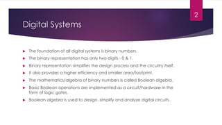
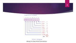
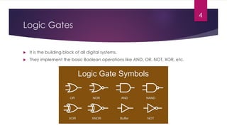
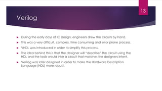
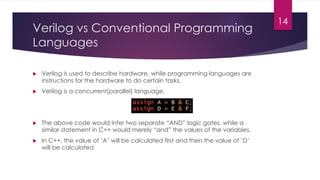
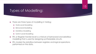
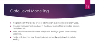
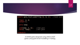
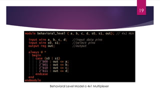
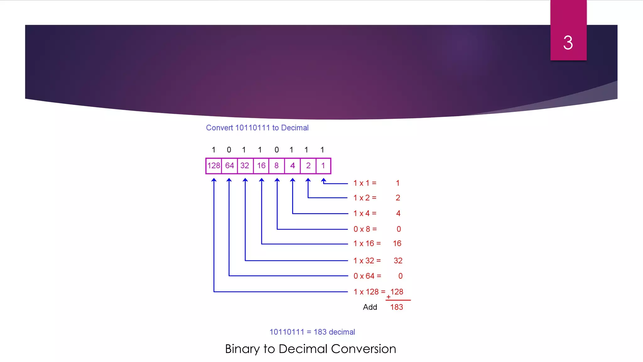
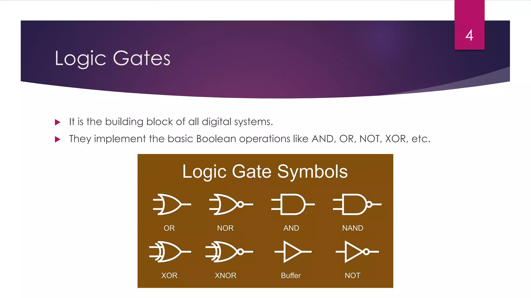
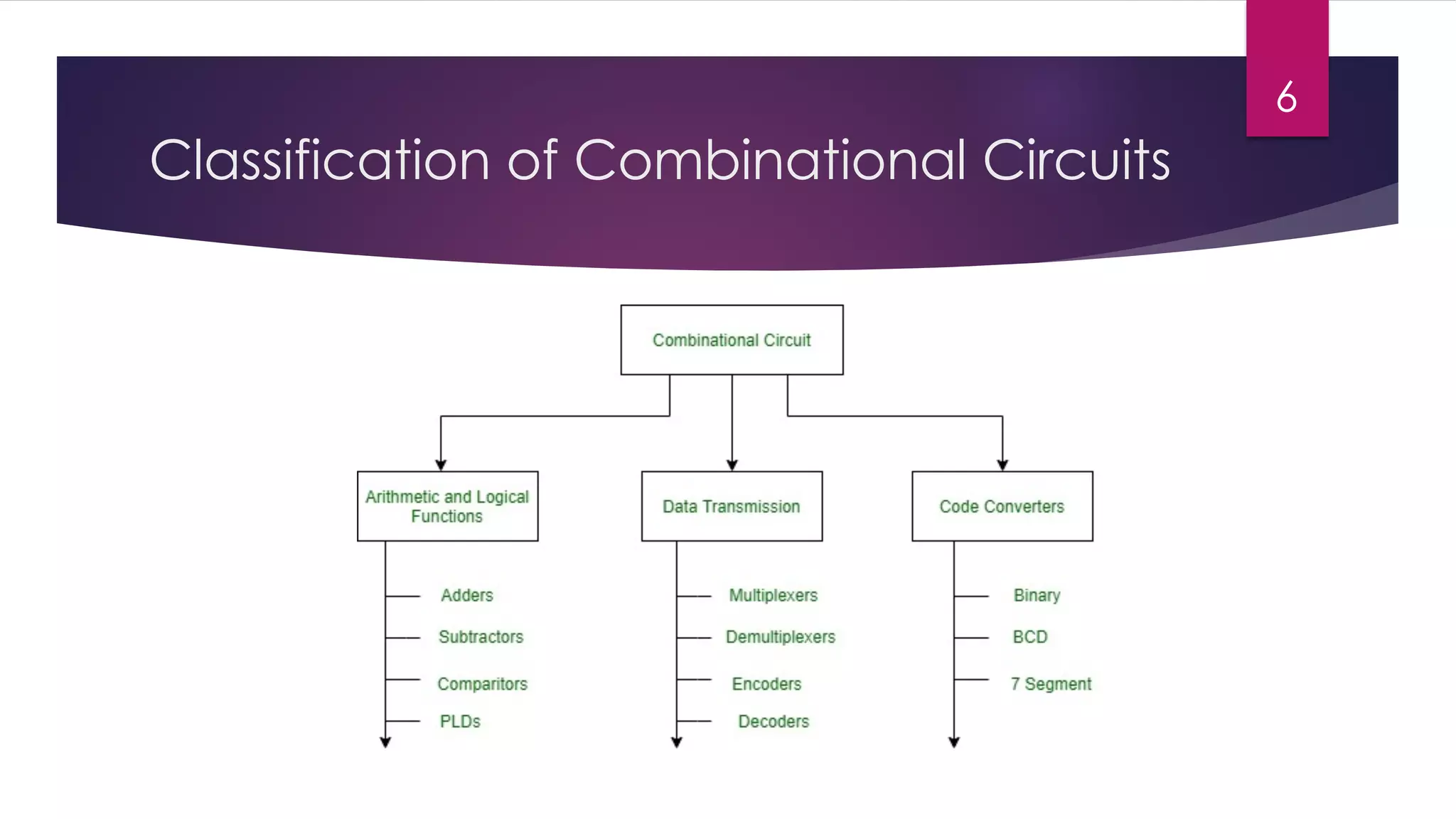
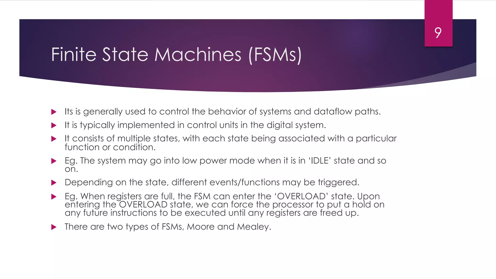
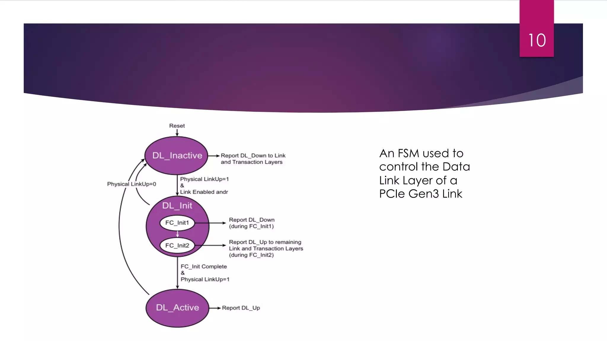
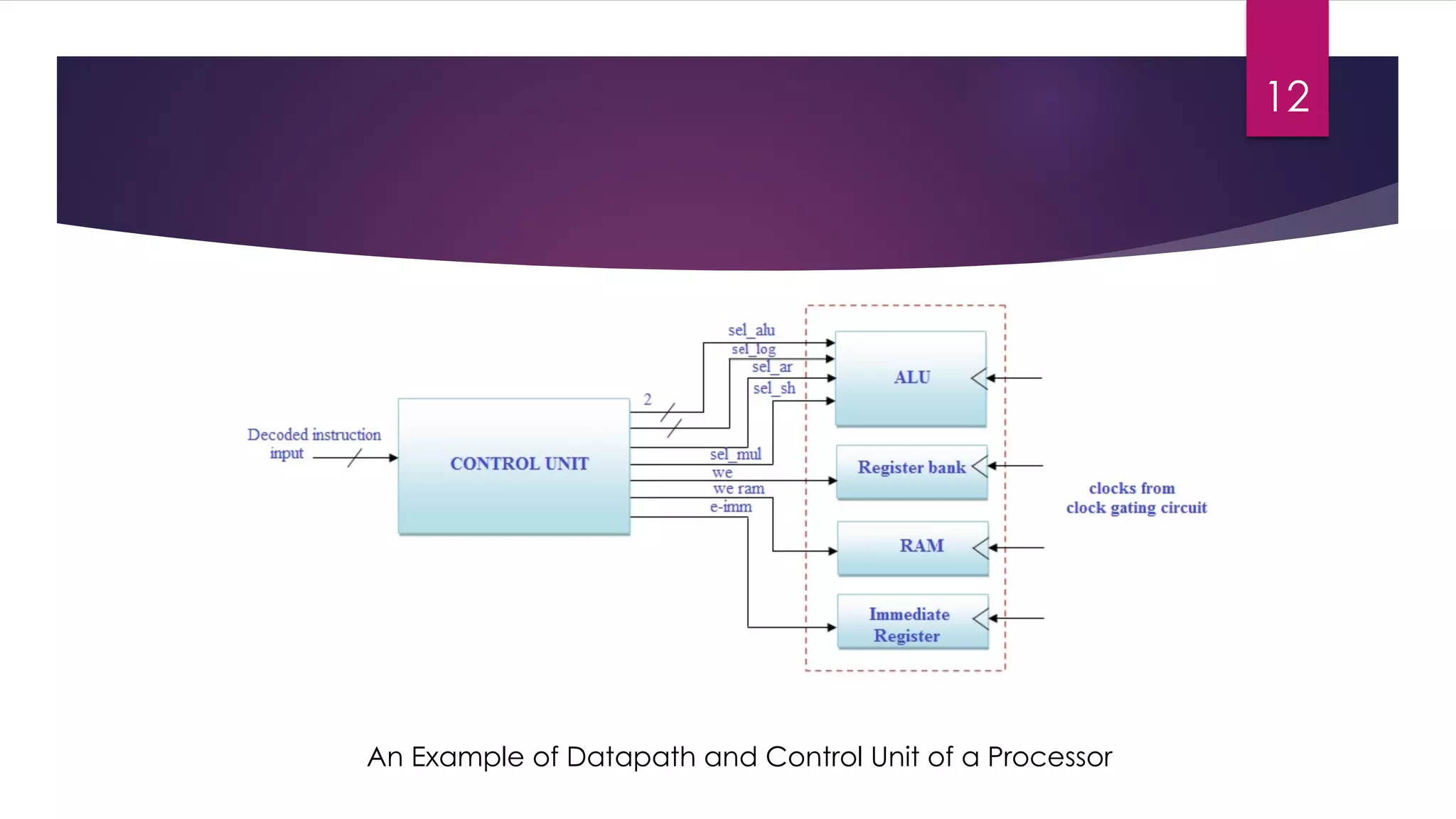
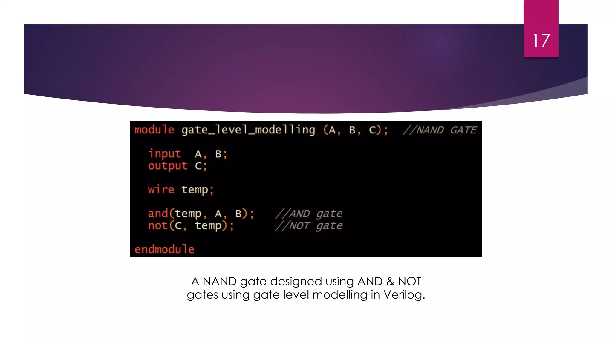
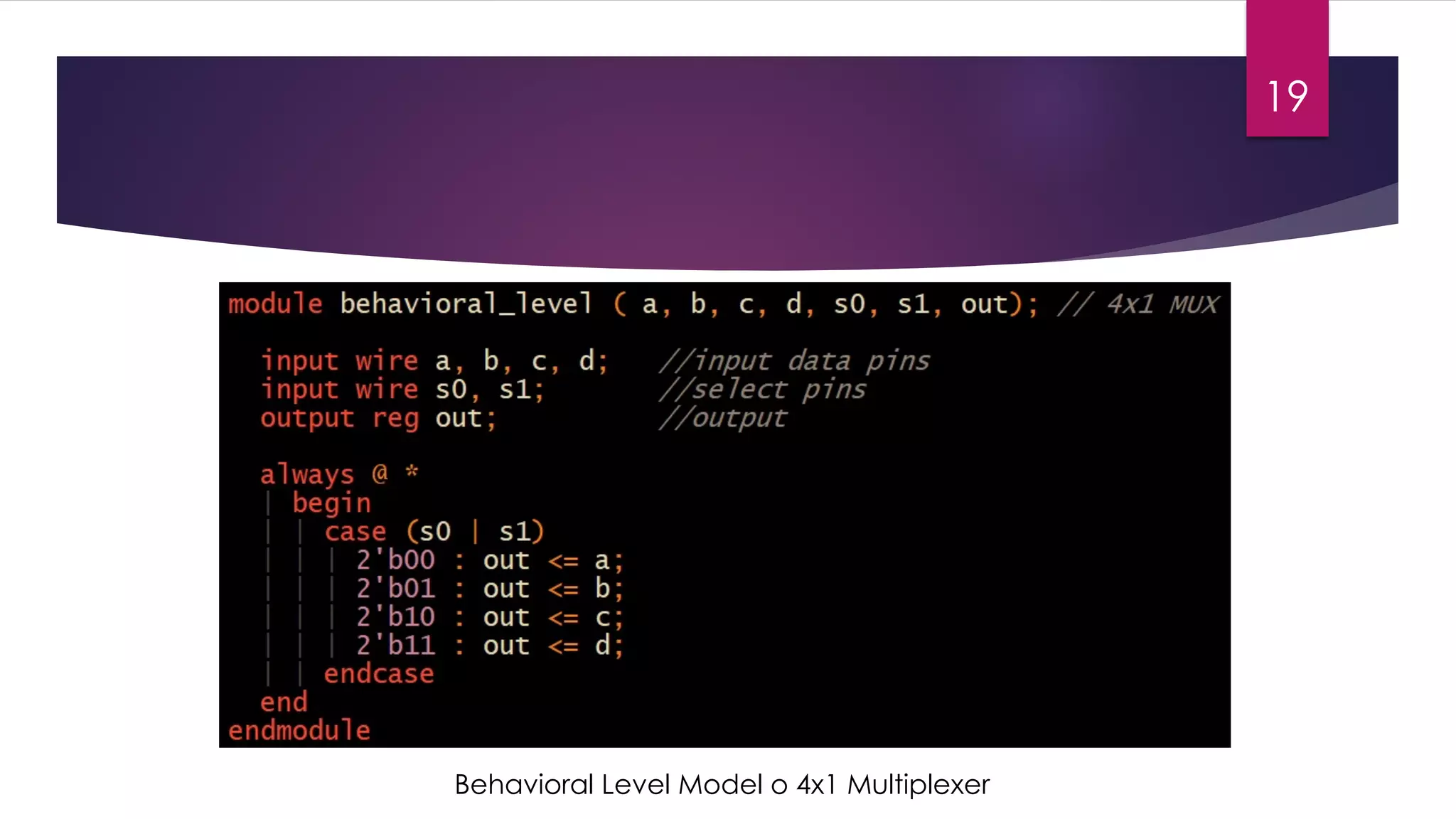
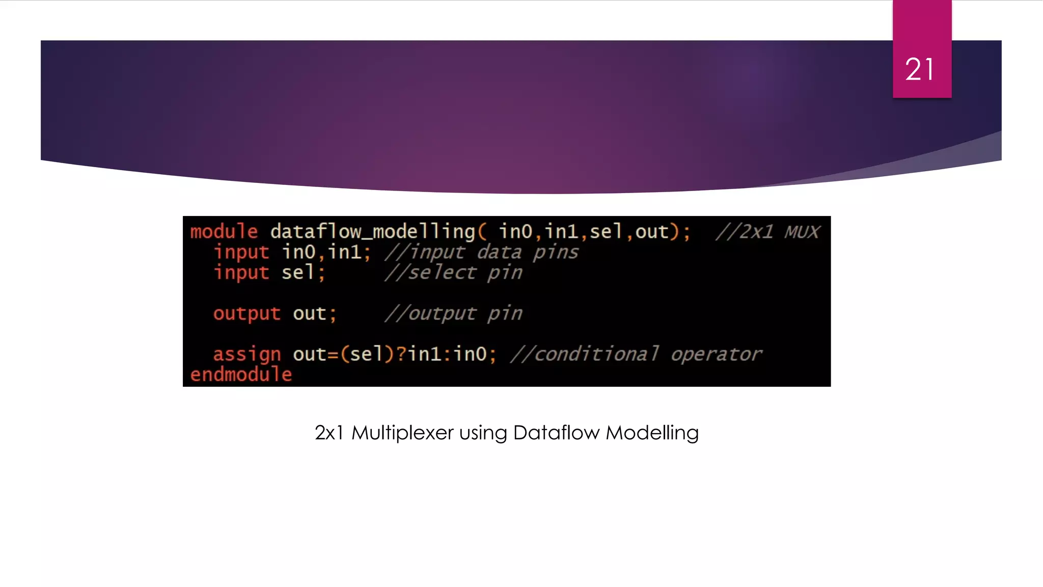
KEMBAR78
Basics of Digital Design and Verilog | PDF
Digital Design & Verilog
PRITHIVIRAJ. R, RITHIK NAMBIAR
SRMIST, KTR.
Digital Systems
u The foundation of all digital systems is binary numbers.
u The binary representation has only two digits - 0 & 1.
u Binary representation simplifies the design process and the circuitry itself.
u It also provides a higher efficiency and smaller area/footprint.
u The mathematics/algebra of binary numbers is called Boolean algebra.
u Basic Boolean operations are implemented as a circuit/hardware in the
form of logic gates.
u Boolean algebra is used to design, simplify and analyze digital circuits.
2
Binary to Decimal Conversion
3
Logic Gates
u It is the building block of all digital systems.
u They implement the basic Boolean operations like AND, OR, NOT, XOR, etc.
4
Combinational Circuits
u The output depends only on a combination of the present inputs.
u Because of its dependence only on the present inputs, there is no
feedback loop involved.
u Examples include adders, multipliers, multiplexers, encoders, PLA, PLDs, etc.
5
Classification of Combinational Circuits
6
Sequential Circuits
u Sequential Circuits the inputs depend on present as well as past inputs.
u Sequential Circuits involve combinational blocks of logic and memory
elements.
u Examples include flip flops, FSM, RAM, etc.
u Sequential Circuits are of two types:
u Synchronous: They output changes are synchronized to edges of the clock
(positive/rising edge or negative/falling edge)
u Asynchronous: The output changes are triggered by the value of the clock(high
or low), i.e., it is level sensitive.
7
8
Asynchronous vs Synchronous Circuits – Timing Diagram
Finite State Machines (FSMs)
u Its is generally used to control the behavior of systems and dataflow paths.
u It is typically implemented in control units in the digital system.
u It consists of multiple states, with each state being associated with a particular
function or condition.
u Eg. The system may go into low power mode when it is in ‘IDLE’ state and so
on.
u Depending on the state, different events/functions may be triggered.
u Eg. When registers are full, the FSM can enter the ‘OVERLOAD’ state. Upon
entering the OVERLOAD state, we can force the processor to put a hold on
any future instructions to be executed until any registers are freed up.
u There are two types of FSMs, Moore and Mealey.
9
10
An FSM used to
control the Data
Link Layer of a
PCIe Gen3 Link
Modern Digital Design
u Modern Digital Design uses the concept of Datapath and Control Units.
u The Datapath include functional blocks like ALUs.
u The Control Units are typically implemented as FSMs.
11
12
An Example of Datapath and Control Unit of a Processor
Verilog
u During the early days of IC Design, engineers drew the circuits by hand.
u This was a very difficult, complex, time consuming and error prone process.
u VHDL was introduced in order to simplify this process.
u The idea behind this is that the designer will “describe” the circuit using the
HDL and the tools would infer a circuit that matches the designers intent.
u Verilog was later designed in order to make the Hardware Description
Language (HDL) more robust.
13
Verilog vs Conventional Programming
Languages
u Verilog is used to describe hardware, while programming languages are
instructions for the hardware to do certain tasks.
u Verilog is a concurrent(parallel) language.
u The above code would infer two separate “AND” logic gates, while a
similar statement in C++ would merely “and” the values of the variables.
u In C++, the value of ‘A’ will be calculated first and then the value of ‘D’
will be calculated
14
Types of Modelling:
u There are three types of modelling in Verilog:
u Gate Level Modelling
u Behavioral Modelling
u Dataflow Modelling
u Switch Level Modelling
u RTL or Register transfer level is a mixture of behavioral and dataflow
modelling that is used for designing synthesizable circuits.
u RTL models the dataflow between registers and logical operations
performed on the data.
15
Gate Level Modelling
u It is practically the lowest level of abstraction as switch level is rarely used.
u It is used to implement modules in the lower levels of hierarchy like adders,
multipliers, etc.
u Here the connection between the pins of the logic gates are manually
specified.
u Netlist obtained from synthesis tools are generally gate level models in
Verilog.
16
A NAND gate designed using AND & NOT
gates using gate level modelling in Verilog.
17
Behavioral Level Modelling
u It is one of the highest level of abstraction provided by Verilog.
u Procedural blocks and ‘reg’ variables are used the describe the behavior
of the intended hardware.
u Other statements like case, if, loops are used to model the behavior of the
hardware.
u It is not necessarily synthesizable.
18
Behavioral Level Model o 4x1 Multiplexer
19
Dataflow Modelling
u This involves the use of operators to model the flow of data in the digital
system, mainly using assign statements.
u It is mainly used for designing combinational circuits.
u It is always synthesizable.
20
2x1 Multiplexer using Dataflow Modelling
21
Switch Level Modelling
u This is the lowest level of modelling in Verilog.
u It is similar to gate level modelling except that connections between the
pins of the transistor is specified(like gate, drain ,etc.)
u It involves the use of transistor primitives.
22
NOT gate using Switch Level Modelling
23
References
u Morris Mano Digital Design 5th edition
u www.chipverify.com
u www.asic-world.com
u PCI Express Technology 3.0 - Mindshare
24
Thank You
25

Basics of Digital Design and Verilog

  • 1.
    Digital Design &Verilog PRITHIVIRAJ. R, RITHIK NAMBIAR SRMIST, KTR.
  • 2.
    Digital Systems u Thefoundation of all digital systems is binary numbers. u The binary representation has only two digits - 0 & 1. u Binary representation simplifies the design process and the circuitry itself. u It also provides a higher efficiency and smaller area/footprint. u The mathematics/algebra of binary numbers is called Boolean algebra. u Basic Boolean operations are implemented as a circuit/hardware in the form of logic gates. u Boolean algebra is used to design, simplify and analyze digital circuits. 2
  • 3.
    Binary to DecimalConversion 3
  • 4.
    Logic Gates u Itis the building block of all digital systems. u They implement the basic Boolean operations like AND, OR, NOT, XOR, etc. 4
  • 5.
    Combinational Circuits u Theoutput depends only on a combination of the present inputs. u Because of its dependence only on the present inputs, there is no feedback loop involved. u Examples include adders, multipliers, multiplexers, encoders, PLA, PLDs, etc. 5
  • 6.
  • 7.
    Sequential Circuits u SequentialCircuits the inputs depend on present as well as past inputs. u Sequential Circuits involve combinational blocks of logic and memory elements. u Examples include flip flops, FSM, RAM, etc. u Sequential Circuits are of two types: u Synchronous: They output changes are synchronized to edges of the clock (positive/rising edge or negative/falling edge) u Asynchronous: The output changes are triggered by the value of the clock(high or low), i.e., it is level sensitive. 7
  • 8.
    8 Asynchronous vs SynchronousCircuits – Timing Diagram
  • 9.
    Finite State Machines(FSMs) u Its is generally used to control the behavior of systems and dataflow paths. u It is typically implemented in control units in the digital system. u It consists of multiple states, with each state being associated with a particular function or condition. u Eg. The system may go into low power mode when it is in ‘IDLE’ state and so on. u Depending on the state, different events/functions may be triggered. u Eg. When registers are full, the FSM can enter the ‘OVERLOAD’ state. Upon entering the OVERLOAD state, we can force the processor to put a hold on any future instructions to be executed until any registers are freed up. u There are two types of FSMs, Moore and Mealey. 9
  • 10.
    10 An FSM usedto control the Data Link Layer of a PCIe Gen3 Link
  • 11.
    Modern Digital Design uModern Digital Design uses the concept of Datapath and Control Units. u The Datapath include functional blocks like ALUs. u The Control Units are typically implemented as FSMs. 11
  • 12.
    12 An Example ofDatapath and Control Unit of a Processor
  • 13.
    Verilog u During theearly days of IC Design, engineers drew the circuits by hand. u This was a very difficult, complex, time consuming and error prone process. u VHDL was introduced in order to simplify this process. u The idea behind this is that the designer will “describe” the circuit using the HDL and the tools would infer a circuit that matches the designers intent. u Verilog was later designed in order to make the Hardware Description Language (HDL) more robust. 13
  • 14.
    Verilog vs ConventionalProgramming Languages u Verilog is used to describe hardware, while programming languages are instructions for the hardware to do certain tasks. u Verilog is a concurrent(parallel) language. u The above code would infer two separate “AND” logic gates, while a similar statement in C++ would merely “and” the values of the variables. u In C++, the value of ‘A’ will be calculated first and then the value of ‘D’ will be calculated 14
  • 15.
    Types of Modelling: uThere are three types of modelling in Verilog: u Gate Level Modelling u Behavioral Modelling u Dataflow Modelling u Switch Level Modelling u RTL or Register transfer level is a mixture of behavioral and dataflow modelling that is used for designing synthesizable circuits. u RTL models the dataflow between registers and logical operations performed on the data. 15
  • 16.
    Gate Level Modelling uIt is practically the lowest level of abstraction as switch level is rarely used. u It is used to implement modules in the lower levels of hierarchy like adders, multipliers, etc. u Here the connection between the pins of the logic gates are manually specified. u Netlist obtained from synthesis tools are generally gate level models in Verilog. 16
  • 17.
    A NAND gatedesigned using AND & NOT gates using gate level modelling in Verilog. 17
  • 18.
    Behavioral Level Modelling uIt is one of the highest level of abstraction provided by Verilog. u Procedural blocks and ‘reg’ variables are used the describe the behavior of the intended hardware. u Other statements like case, if, loops are used to model the behavior of the hardware. u It is not necessarily synthesizable. 18
  • 19.
    Behavioral Level Modelo 4x1 Multiplexer 19
  • 20.
    Dataflow Modelling u Thisinvolves the use of operators to model the flow of data in the digital system, mainly using assign statements. u It is mainly used for designing combinational circuits. u It is always synthesizable. 20
  • 21.
    2x1 Multiplexer usingDataflow Modelling 21
  • 22.
    Switch Level Modelling uThis is the lowest level of modelling in Verilog. u It is similar to gate level modelling except that connections between the pins of the transistor is specified(like gate, drain ,etc.) u It involves the use of transistor primitives. 22
  • 23.
    NOT gate usingSwitch Level Modelling 23
  • 24.
    References u Morris ManoDigital Design 5th edition u www.chipverify.com u www.asic-world.com u PCI Express Technology 3.0 - Mindshare 24
  • 25.