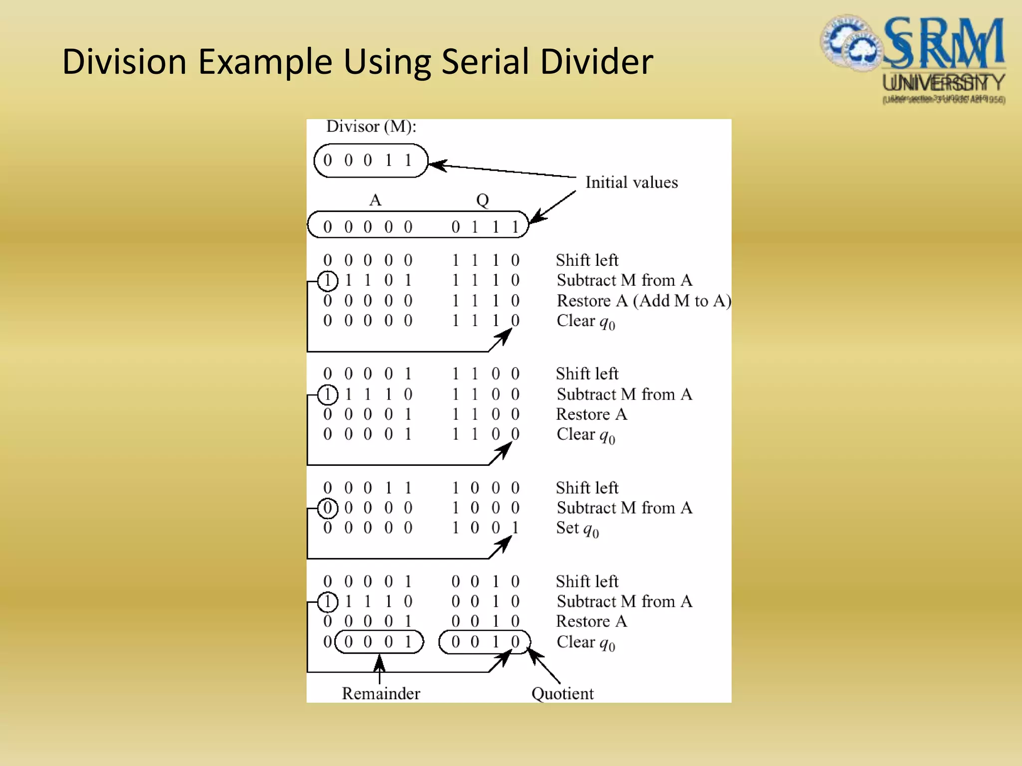
BOOTH ALGO, DIVISION(RESTORING _ NON RESTORING) etc etc
The document discusses various aspects of central processing unit (CPU) architecture and arithmetic operations. It covers the main components of a CPU - the arithmetic logic unit (ALU), control unit, and registers. It then describes different data representation methods including fixed-point and floating-point numbers. Various arithmetic operations for both types of numbers such as addition, subtraction, multiplication, and division are explained. Different adder designs like ripple-carry adder and carry lookahead adder are also summarized.
Introduction to CPU, covering ALU, fixed and floating point arithmetic, pipelining.
Details on ALU, data formats including numeric and non-numeric data.
Overview of conventional digit sets and positional number systems, classification of numbers.
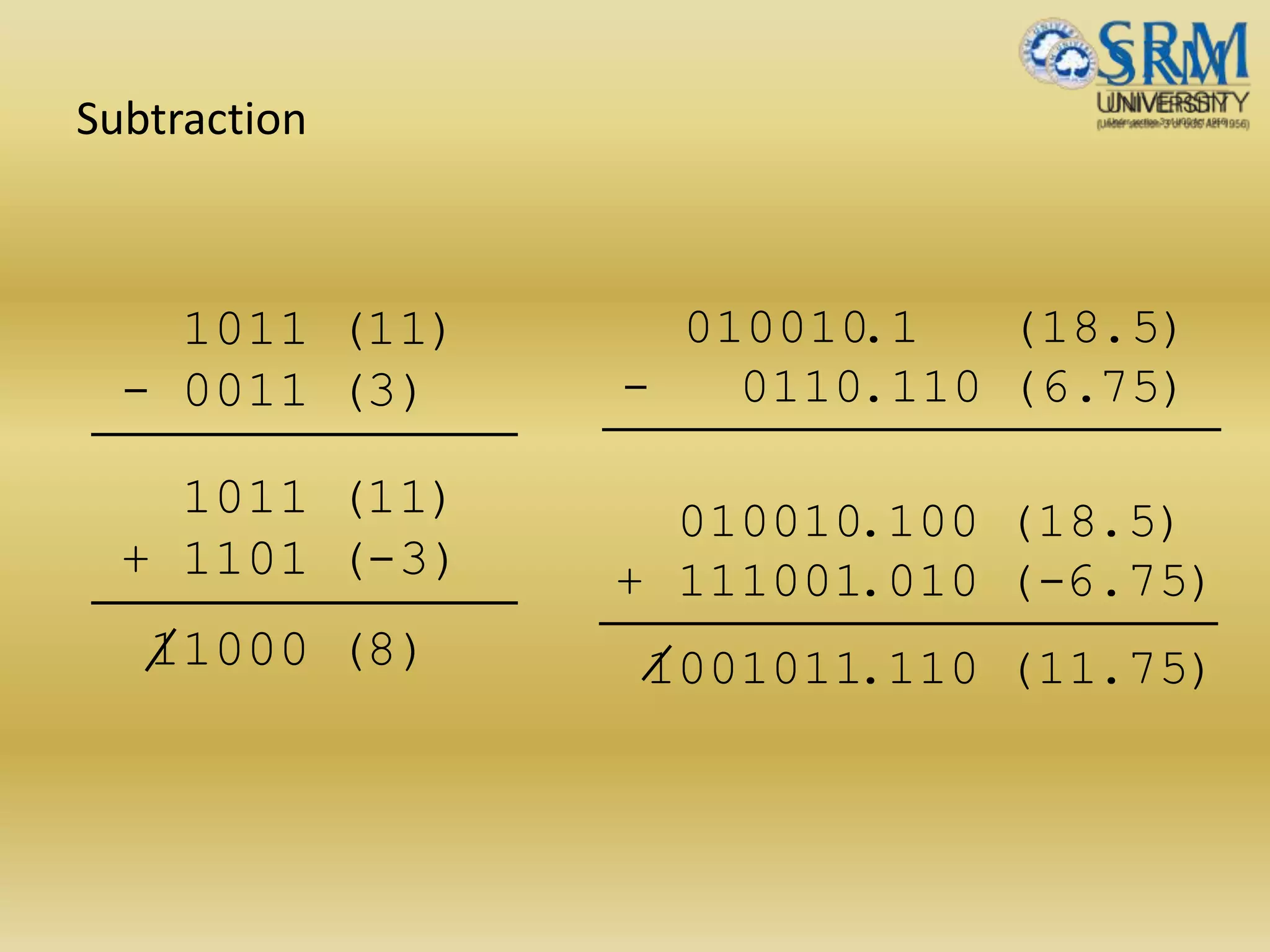
Explanation of fixed point representation, arithmetic operations including addition and subtraction.
Illustrations of unsigned and signed integer representations and basic operations in fixed point arithmetic.
Description of floating point representation similar to scientific notation; components include significand and exponent.
Detailed examination of floating point arithmetic and computations including addition, multiplication, and division.
Design principles of adders, ALUs, exploration of carry propagation, ripple-carry, and lookahead mechanisms.Cycle phases for instruction execution including fetching, decoding, executing, and result returning.
In-depth explanation of instruction pipelining and its effect on performance in CPU design.
BOOTH ALGO, DIVISION(RESTORING _ NON RESTORING) etc etc
1.
UNIT-II CENTRAL PROCESSINGUNIT
•INTODUCTION
•ARITHMETIC LOGIC UNIT
•FIXED POINT ARITHMETIC
•FLOATING POINT ARITHMETIC
•EXECUTION OF A COMPLETE INSTRUCTION
•BASIC CONCEPTS OF PIPELINING
2.
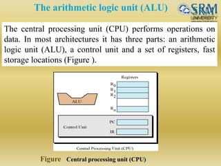
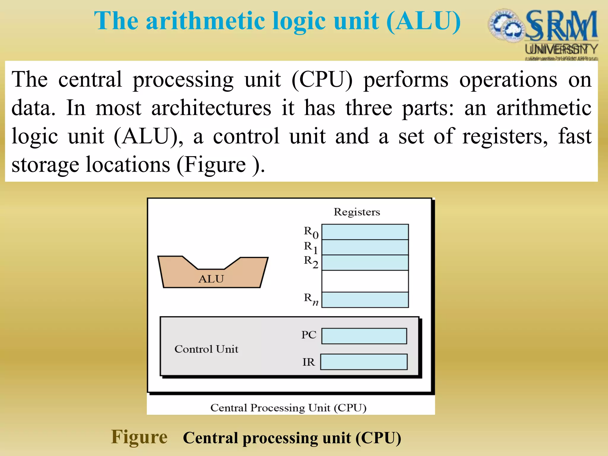
The arithmetic logicunit (ALU)
The central processing unit (CPU) performs operations on
data. In most architectures it has three parts: an arithmetic
logic unit (ALU), a control unit and a set of registers, fast
storage locations (Figure ).
Figure Central processing unit (CPU)
3.
Data Representation
• Thebasic form of information handled by
a computer are instructions and data
• Data can be in the form of numbers or
nonnumeric data
• Data in the number form can further
classified as fixed point and floating point
4.
Digit Sets andEncodings
Conventional and unconventional digit sets
Decimal digits in [0, 9]; 4-bit BCD, 8-bit ASCII
Hexadecimal, or hex for short: digits 0-9 & a-f
Conventional digit set for radix r is [0, r – 1]
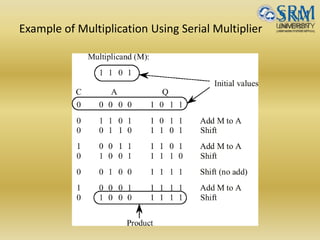
Conventional binary digit set in [0, 1]
5.
Positional Number Systems
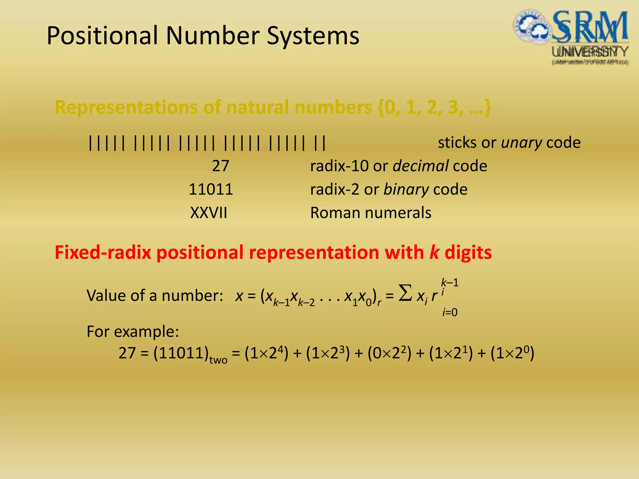
Representationsof natural numbers {0, 1, 2, 3, …}
||||| ||||| ||||| ||||| ||||| || sticks or unary code
27 radix-10 or decimal code
11011 radix-2 or binary code
XXVII Roman numerals
Fixed-radix positional representation with k digits
Value of a number: x = (xk–1xk–2 . . . x1x0)r = S xi r i
For example:
27 = (11011)two = (124) + (123) + (022) + (121) + (120)
k–1
i=0
6.
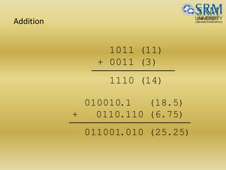
Fixed Point Representation
•Fixed point number actually symbolizes
the real data types.
• As radix point is fixed ,the number system
is fixed point number system
• Fixed point numbers are those which have
a defined numbers after and before the
decimal point.
7.
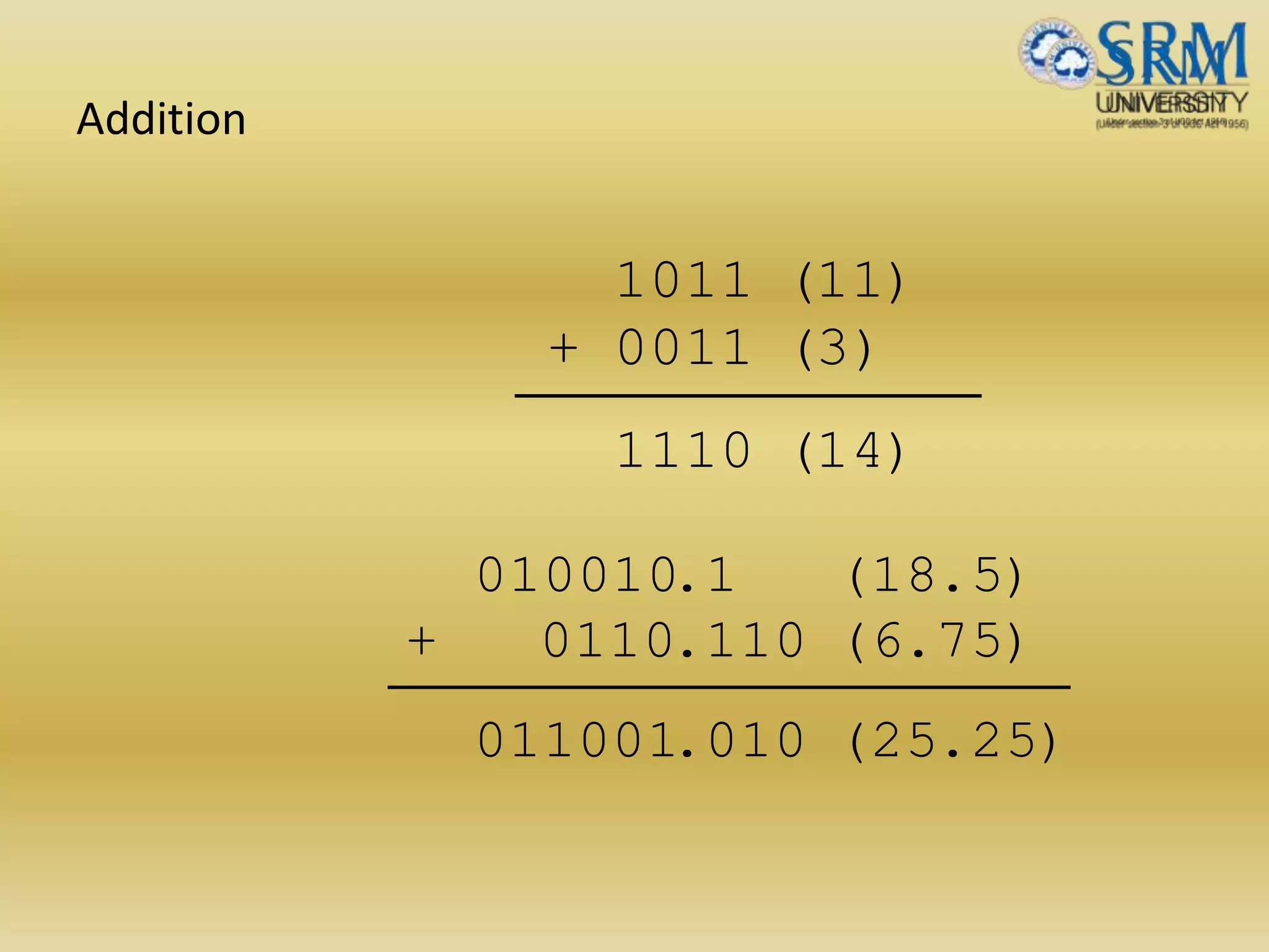
Fixed-Point Numbers
Positional representation:k whole and l fractional digits
Value of a number: x = (xk–1xk–2 . . .x1x0 .x–1x–2 . . . x–l )r = S xi r i
For example:
2.375 = (10.011)two = (121) + (020) + (02-1) + (12-2) + (12-3)
Numbers in the range [0, rk – ulp] representable, where ulp = r–l
Fixed-point arithmetic same as integer arithmetic
(radix point implied, not explicit)
Two’s complement properties (including sign change) hold here as well:
(01.011)2’s-compl = (–021) + (120) + (02–1) + (12–2) + (12–3) = +1.375
(11.011)2’s-compl = (–121) + (120) + (02–1) + (12–2) + (12–3) = –0.625
8.
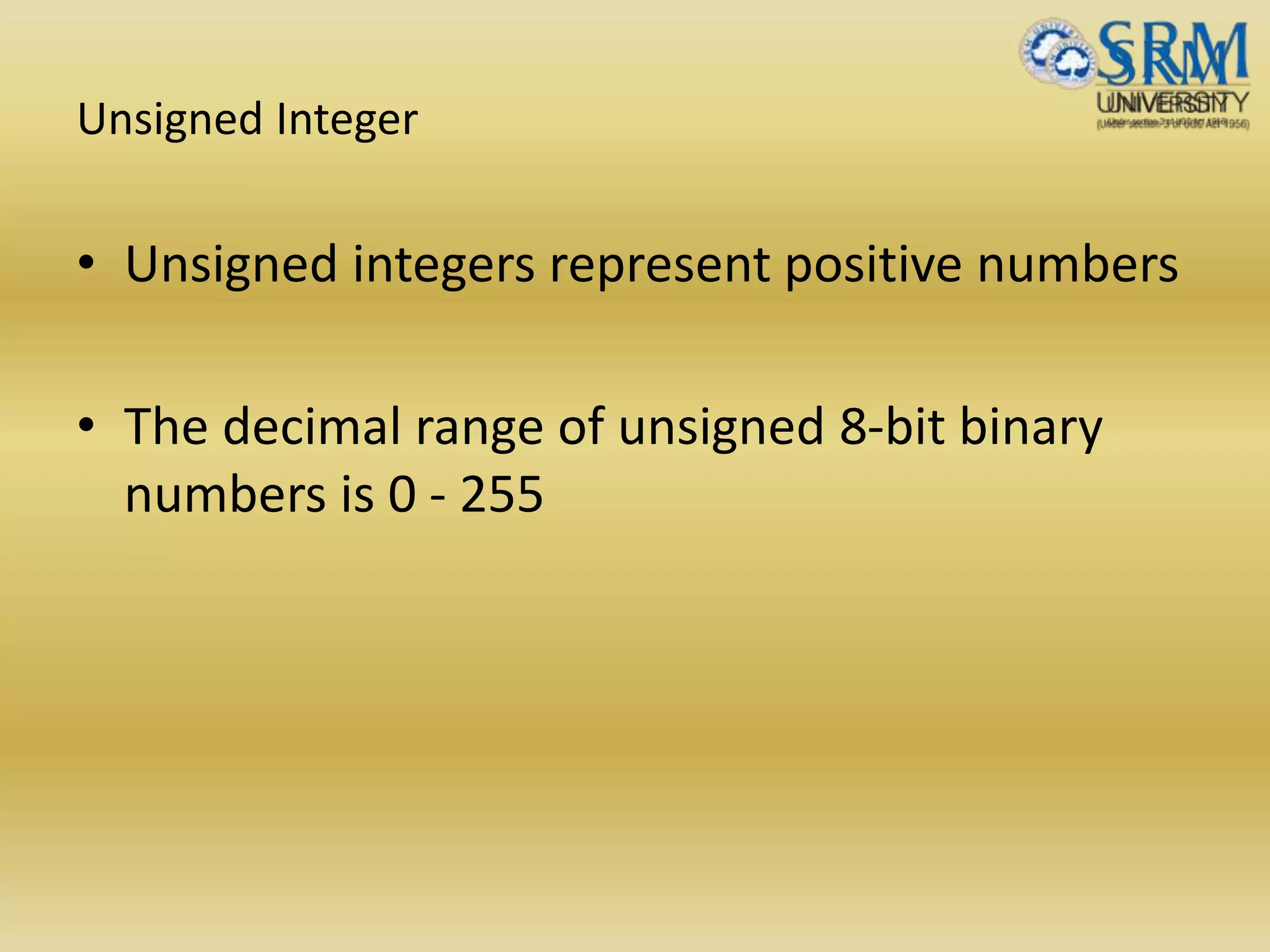
Unsigned Integer
• Unsignedintegers represent positive numbers
• The decimal range of unsigned 8-bit binary
numbers is 0 - 255
9.
Unsigned Binary Integers
Schematicrepresentation of 4-bit code for integers in [0,
15].
0000
00011111
00101110
00111101
01001100
1000
01011011
01101010
01111001
0
1
2
3
4
5
6
7
15
11
14
13
12
8
9
10
Inside: Natural number
Outside: 4-bit encoding
0
1
2
3
15
4
5
6
789
Turn x notches
counterclockwise
to add x
Turn y notches
clockwise
to subtract y
11
14
13
12
10
10.
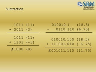
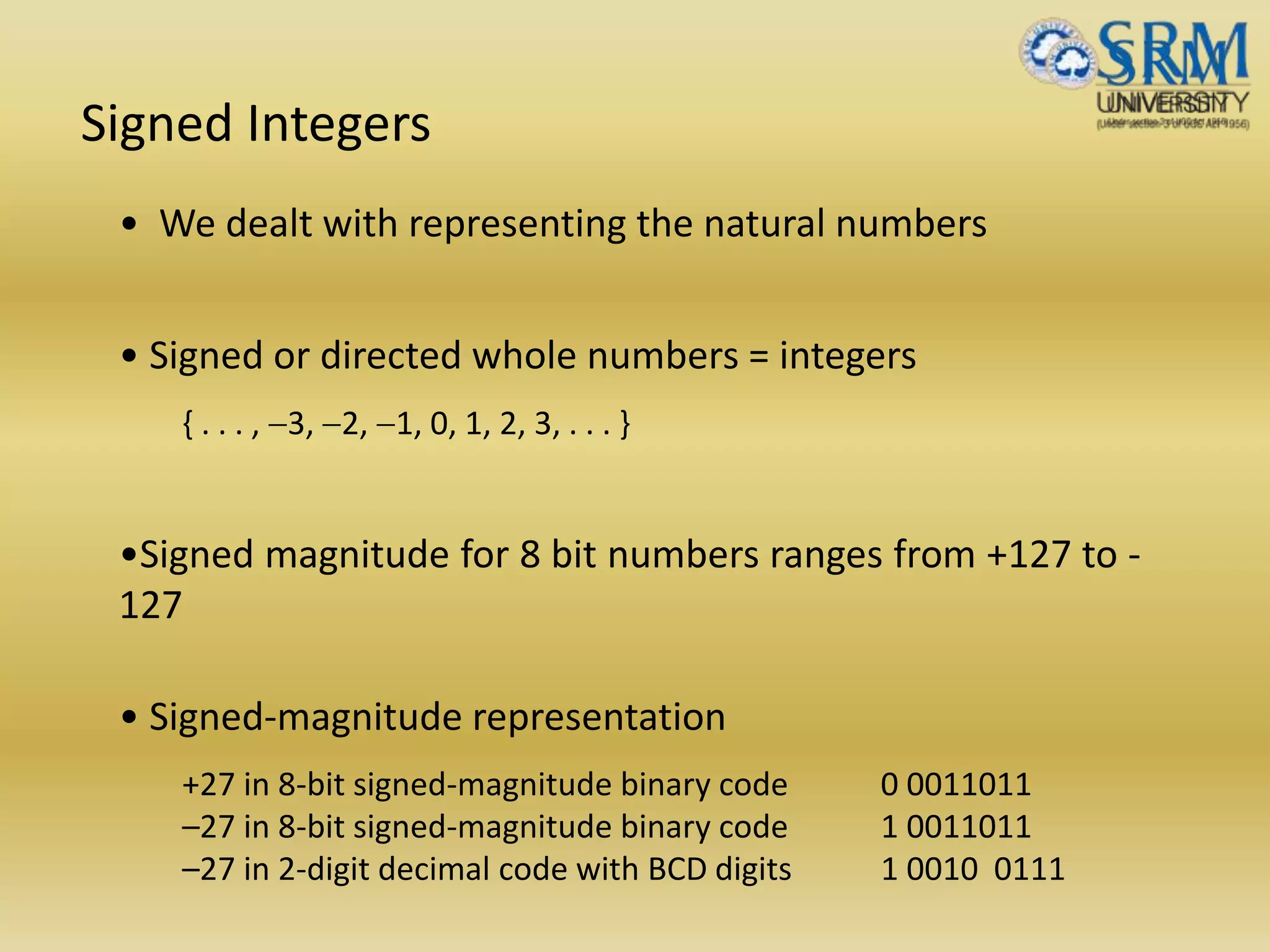
Signed Integers
• Wedealt with representing the natural numbers
• Signed or directed whole numbers = integers
{ . . . , -3, -2, -1, 0, 1, 2, 3, . . . }
•Signed magnitude for 8 bit numbers ranges from +127 to -
127
• Signed-magnitude representation
+27 in 8-bit signed-magnitude binary code 0 0011011
–27 in 8-bit signed-magnitude binary code 1 0011011
–27 in 2-digit decimal code with BCD digits 1 0010 0111
11.
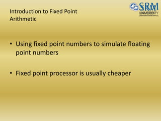
Introduction to FixedPoint
Arithmetic
• Using fixed point numbers to simulate floating
point numbers
• Fixed point processor is usually cheaper
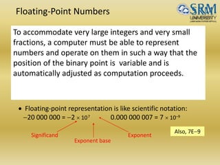
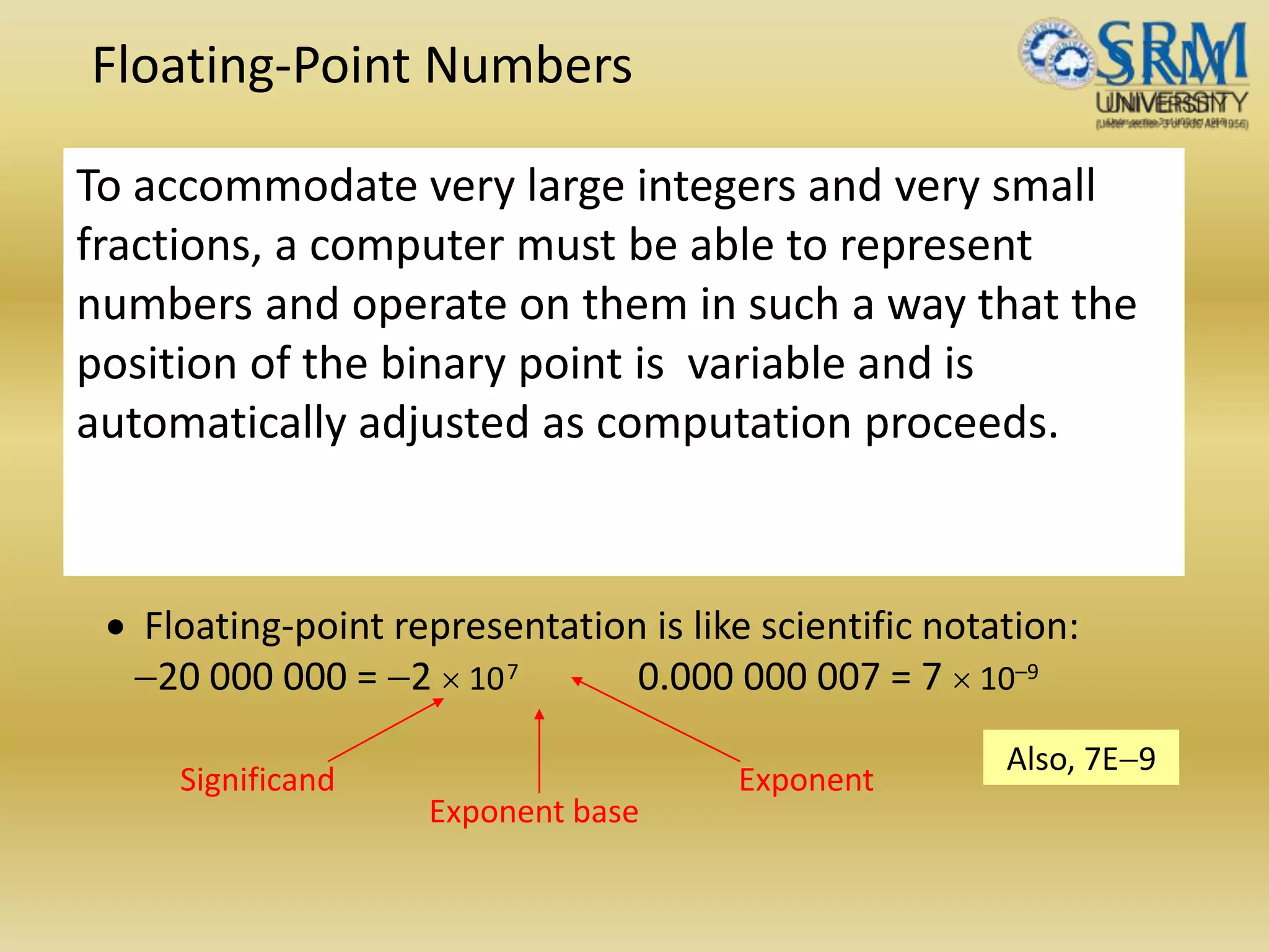
Floating-Point Numbers
Floating-pointrepresentation is like scientific notation:
-20 000 000 = -2 107 0.000 000 007 = 7 10–9
To accommodate very large integers and very small
fractions, a computer must be able to represent
numbers and operate on them in such a way that the
position of the binary point is variable and is
automatically adjusted as computation proceeds.
Significand Exponent
Exponent base
Also, 7E-9
19.
Floating-point Computations
• Representation:(fraction, exponent) Has three fields:
sign, significant digits and exponent
eg.111101.100110 1.11101100110*25
• Value representation = +/- M*2 E’-127
In case of a 32 bit number 1 bit represents sign
8 bits represents exponent E’=E +127(bias) [ excess 127
format]
23 bits represents Mantissa
20.
Floating-point Computations
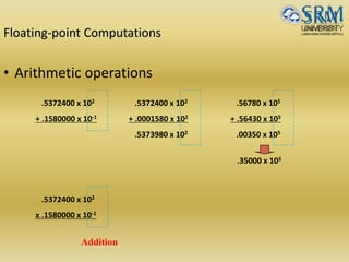
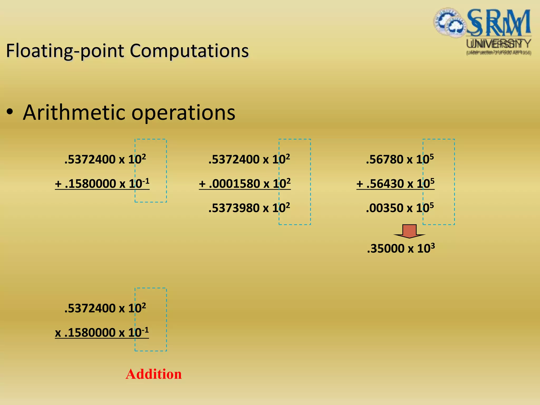
• Arithmeticoperations
.5372400 x 102
+ .1580000 x 10-1
.5372400 x 102
+ .0001580 x 102
.5373980 x 102
.56780 x 105
+ .56430 x 105
.00350 x 105
.35000 x 103
.5372400 x 102
x .1580000 x 10-1
Addition
21.
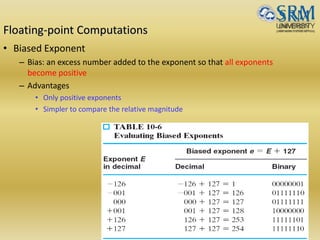
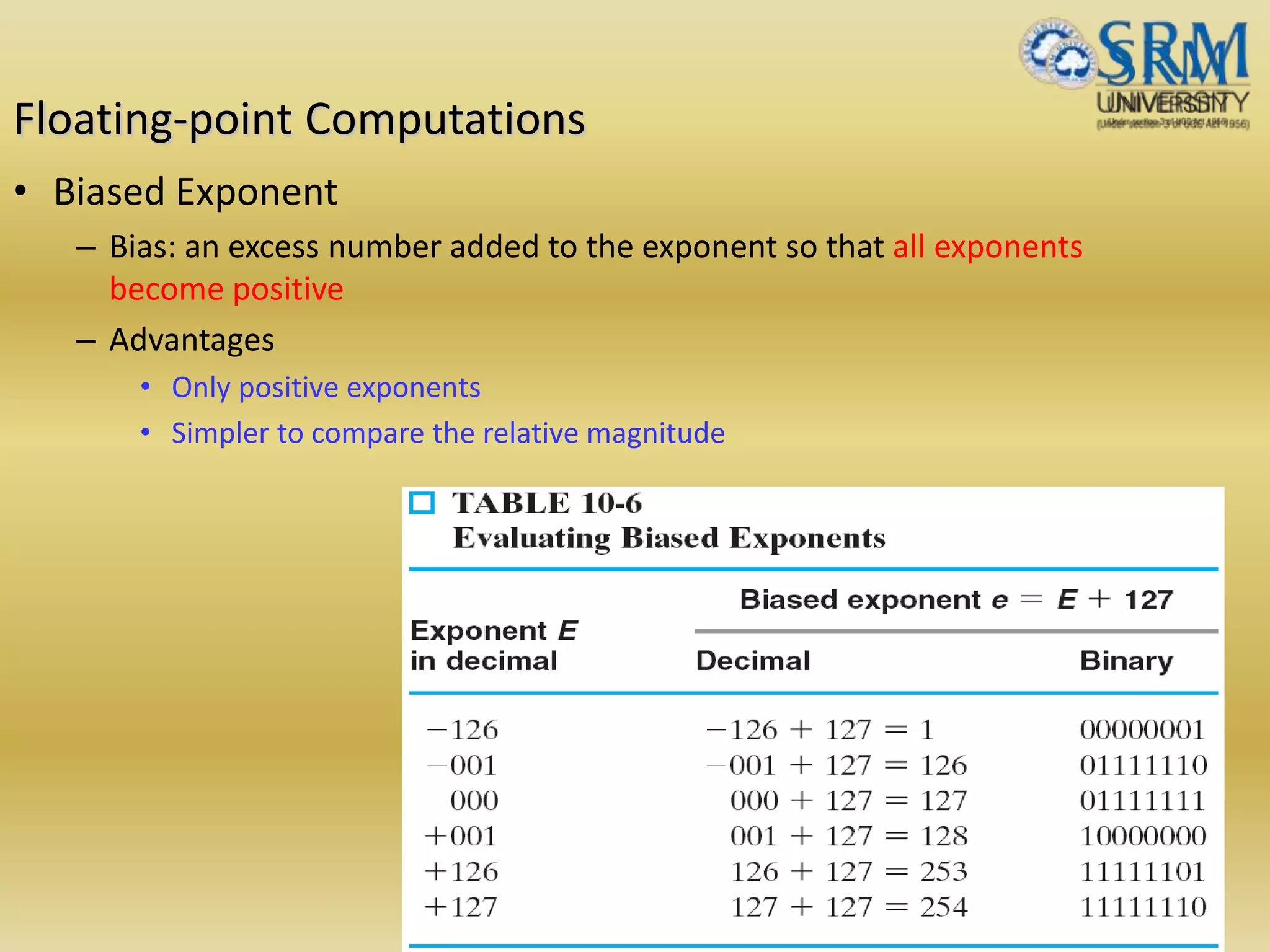
Floating-point Computations
• BiasedExponent
– Bias: an excess number added to the exponent so that all exponents
become positive
– Advantages
• Only positive exponents
• Simpler to compare the relative magnitude
22.
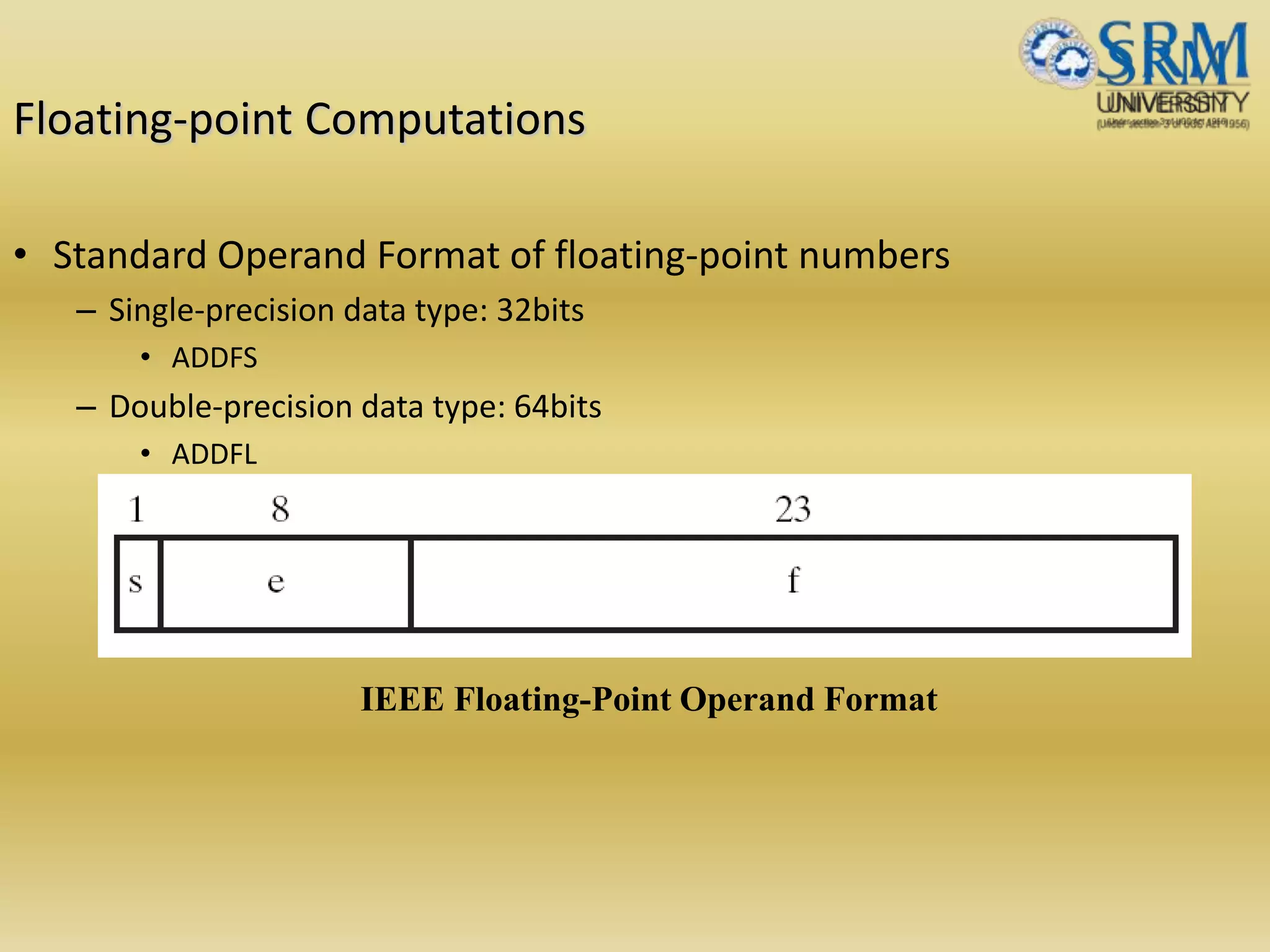
Floating-point Computations
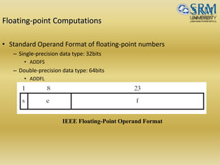
• StandardOperand Format of floating-point numbers
– Single-precision data type: 32bits
• ADDFS
– Double-precision data type: 64bits
• ADDFL
IEEE Floating-Point Operand Format
23.
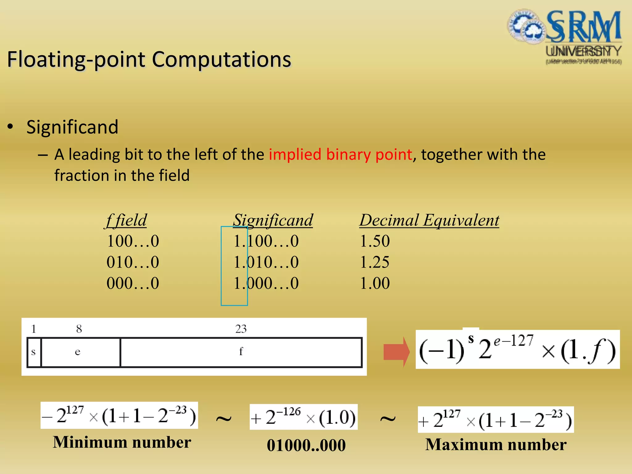
Floating-point Computations
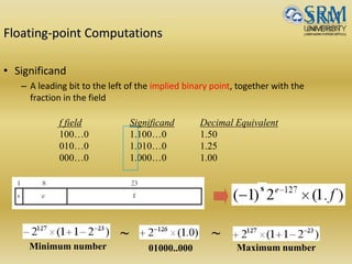
• Significand
–A leading bit to the left of the implied binary point, together with the
fraction in the field
f field Significand Decimal Equivalent
100…0 1.100…0 1.50
010…0 1.010…0 1.25
000…0 1.000…0 1.00
~ ~
s
Minimum number Maximum number01000..000
24.
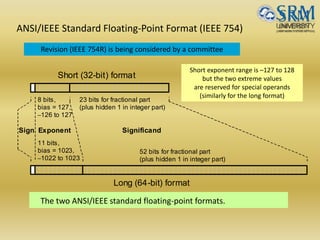
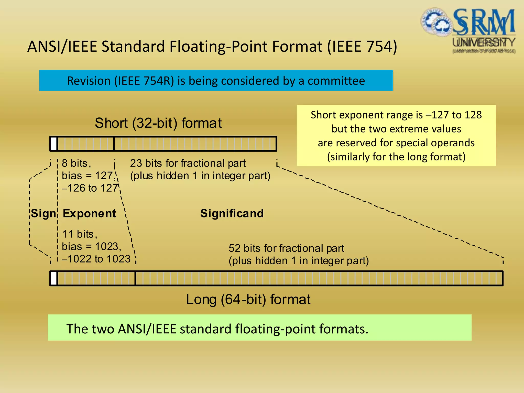
ANSI/IEEE Standard Floating-PointFormat (IEEE 754)
The two ANSI/IEEE standard floating-point formats.
Short (32-bit) format
Long (64-bit) format
Sign Exponent Significand
8 bits,
bias = 127,
–126 to 127
11 bits,
bias = 1023,
–1022 to 1023
52 bits for fractional part
(plus hidden 1 in integer part)
23 bits for fractional part
(plus hidden 1 in integer part)
Short exponent range is –127 to 128
but the two extreme values
are reserved for special operands
(similarly for the long format)
Revision (IEEE 754R) is being considered by a committee
25.
Short and LongIEEE 754 Formats: Features
Table Some features of ANSI/IEEE standard floating-point formats
Feature Single/Short Double/Long
Word width in bits 32 64
Significand in bits 23 + 1 hidden 52 + 1 hidden
Significand range [1, 2 – 2–23] [1, 2 – 2–52]
Exponent bits 8 11
Exponent bias 127 1023
Zero (±0) e + bias = 0, f = 0 e + bias = 0, f = 0
Denormal e + bias = 0, f ≠ 0
represents ±0.f 2–126
e + bias = 0, f ≠ 0
represents ±0.f 2–1022
Infinity (∞) e + bias = 255, f = 0 e + bias = 2047, f = 0
Not-a-number (NaN) e + bias = 255, f ≠ 0 e + bias = 2047, f ≠ 0
Ordinary number e + bias [1, 254]
e [–126, 127]
represents 1.f 2e
e + bias [1, 2046]
e [–1022, 1023]
represents 1.f 2e
min 2–126 1.2 10–38 2–1022 2.2 10–308
max 2128 3.4 1038 21024 1.8 10308
26.
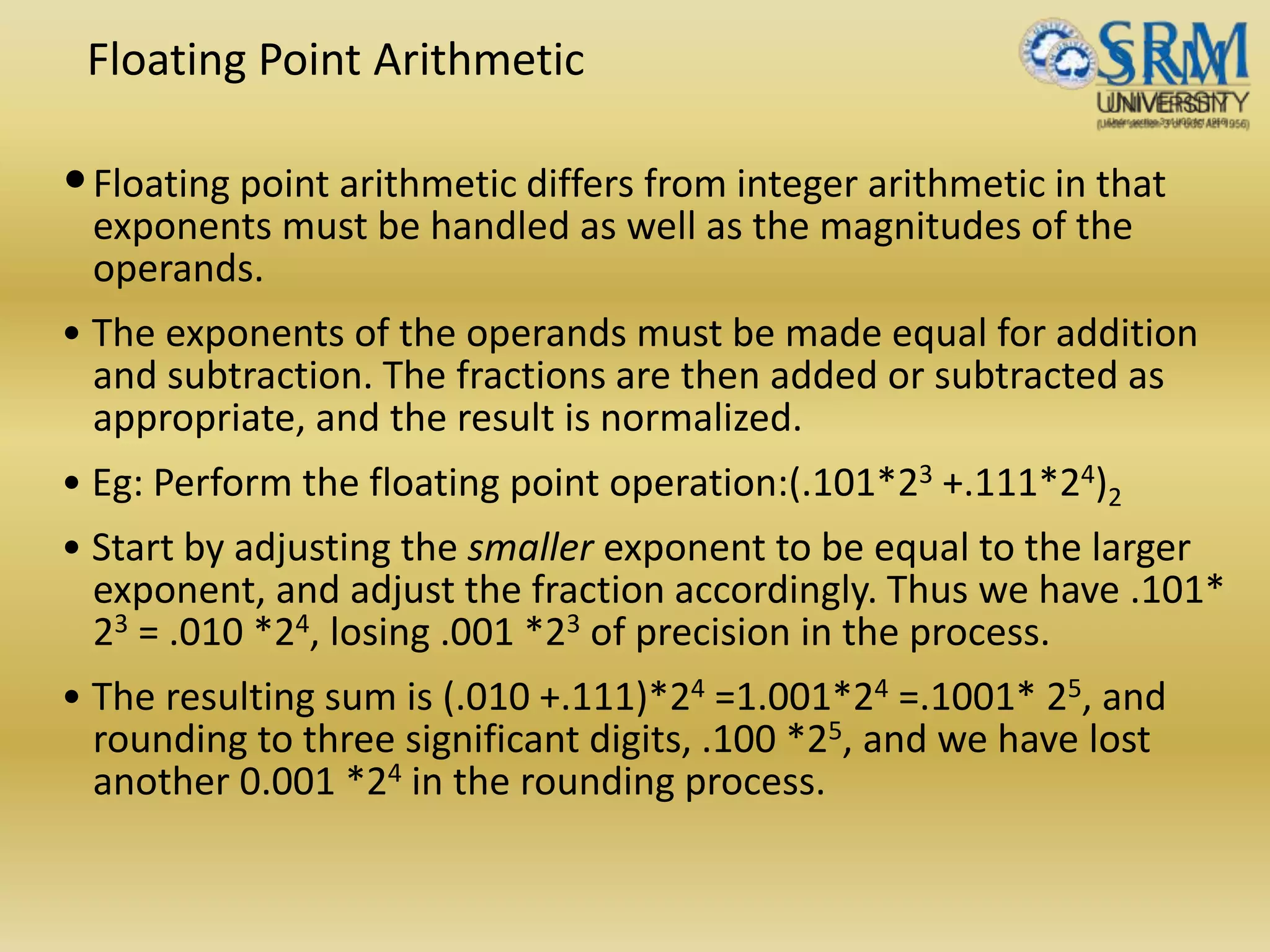
Floating Point Arithmetic
•Floatingpoint arithmetic differs from integer arithmetic in that
exponents must be handled as well as the magnitudes of the
operands.
• The exponents of the operands must be made equal for addition
and subtraction. The fractions are then added or subtracted as
appropriate, and the result is normalized.
• Eg: Perform the floating point operation:(.101*23 +.111*24)2
• Start by adjusting the smaller exponent to be equal to the larger
exponent, and adjust the fraction accordingly. Thus we have .101*
23 = .010 *24, losing .001 *23 of precision in the process.
• The resulting sum is (.010 +.111)*24 =1.001*24 =.1001* 25, and
rounding to three significant digits, .100 *25, and we have lost
another 0.001 *24 in the rounding process.
27.
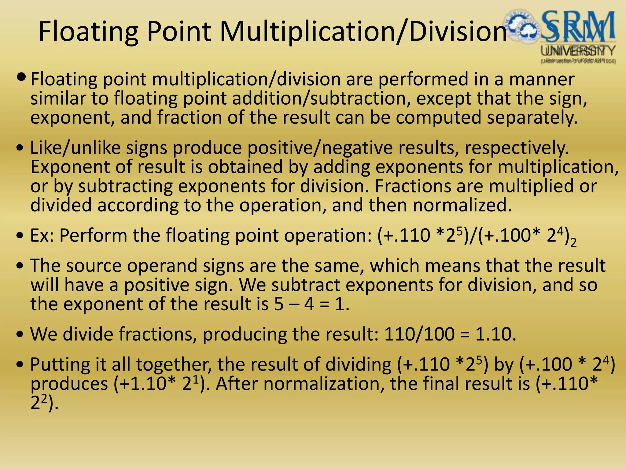
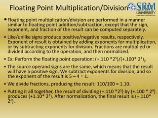
Floating Point Multiplication/Division
•Floatingpoint multiplication/division are performed in a manner
similar to floating point addition/subtraction, except that the sign,
exponent, and fraction of the result can be computed separately.
• Like/unlike signs produce positive/negative results, respectively.
Exponent of result is obtained by adding exponents for multiplication,
or by subtracting exponents for division. Fractions are multiplied or
divided according to the operation, and then normalized.
• Ex: Perform the floating point operation: (+.110 *25)/(+.100* 24)2
• The source operand signs are the same, which means that the result
will have a positive sign. We subtract exponents for division, and so
the exponent of the result is 5 – 4 = 1.
• We divide fractions, producing the result: 110/100 = 1.10.
• Putting it all together, the result of dividing (+.110 *25) by (+.100 * 24)
produces (+1.10* 21). After normalization, the final result is (+.110*
22).
28.
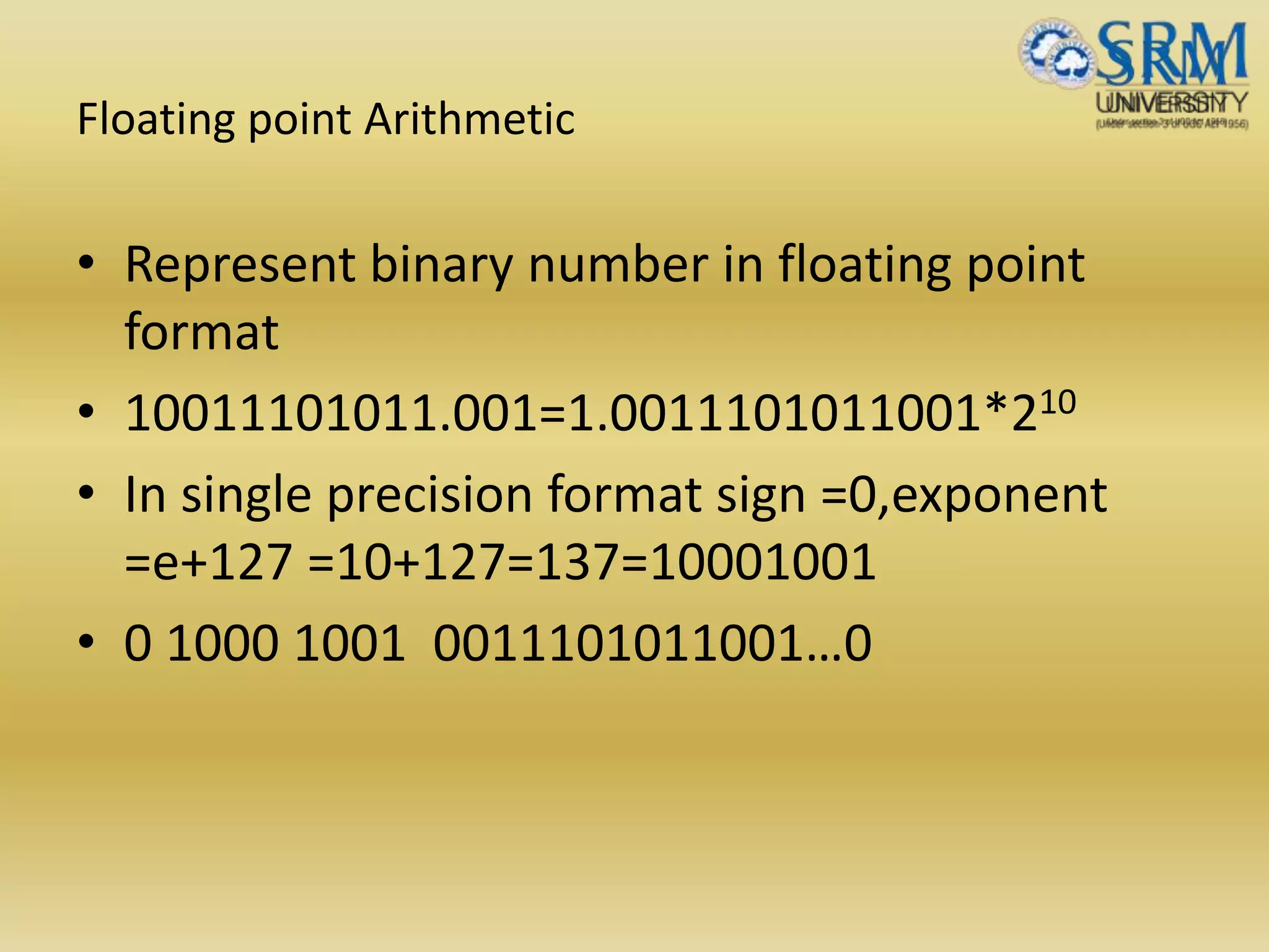
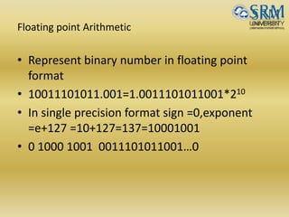
Floating point Arithmetic
•Represent binary number in floating point
format
• 10011101011.001=1.0011101011001*210
• In single precision format sign =0,exponent
=e+127 =10+127=137=10001001
• 0 1000 1001 0011101011001…0
29.
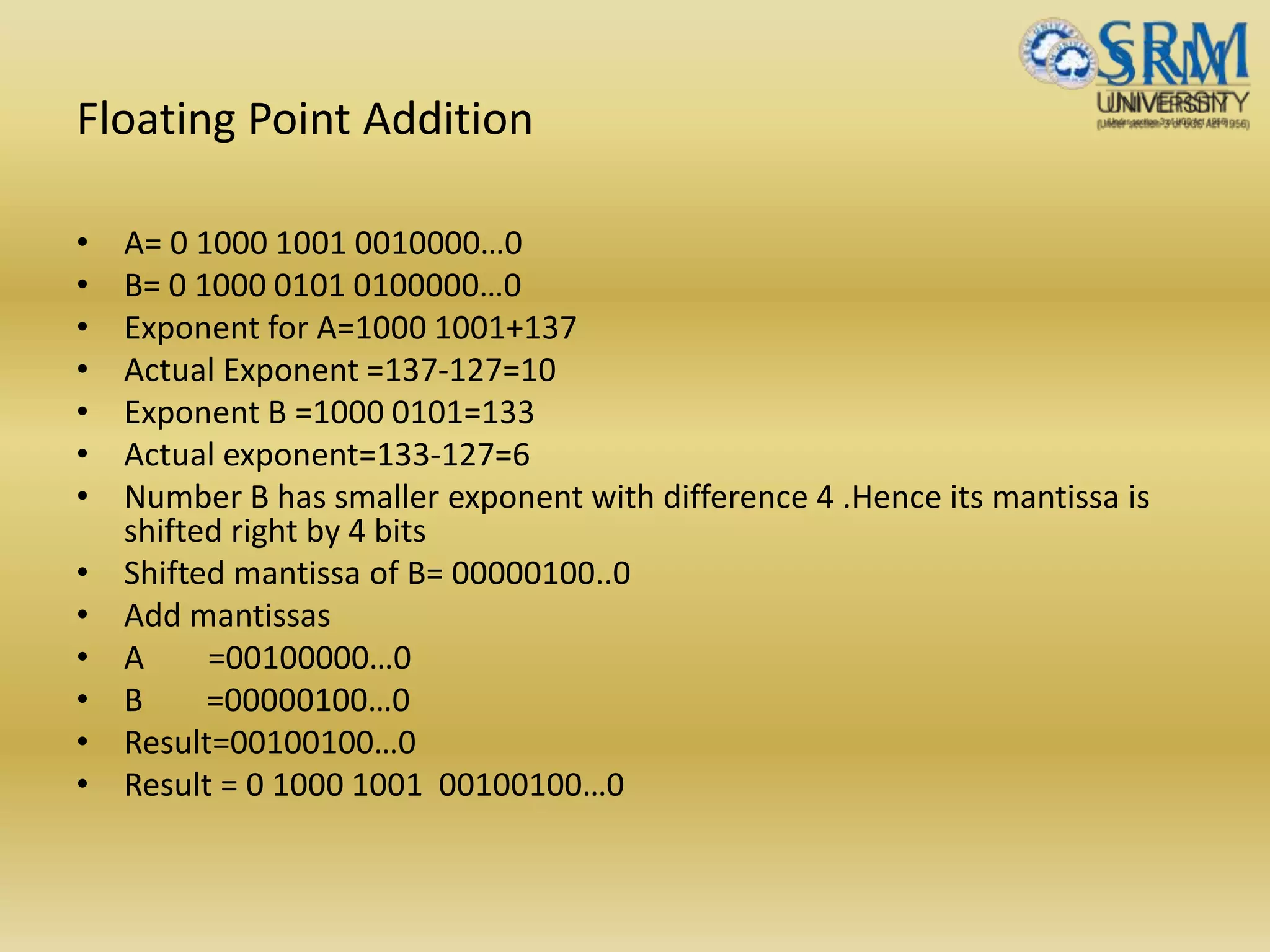
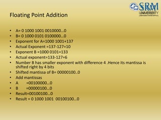
Floating Point Addition
•A= 0 1000 1001 0010000…0
• B= 0 1000 0101 0100000…0
• Exponent for A=1000 1001+137
• Actual Exponent =137-127=10
• Exponent B =1000 0101=133
• Actual exponent=133-127=6
• Number B has smaller exponent with difference 4 .Hence its mantissa is
shifted right by 4 bits
• Shifted mantissa of B= 00000100..0
• Add mantissas
• A =00100000…0
• B =00000100…0
• Result=00100100…0
• Result = 0 1000 1001 00100100…0
30.
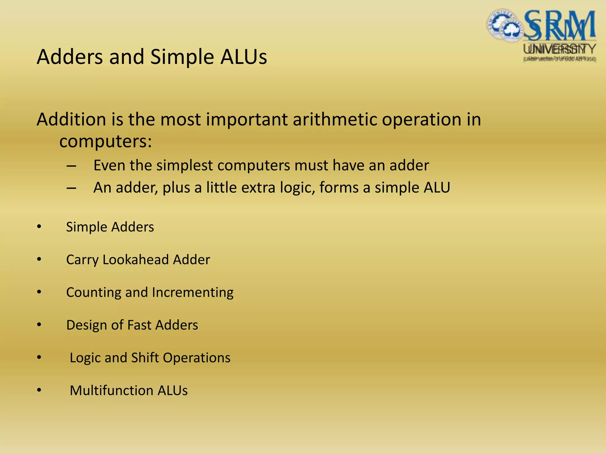
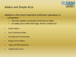
Adders and SimpleALUs
Addition is the most important arithmetic operation in
computers:
– Even the simplest computers must have an adder
– An adder, plus a little extra logic, forms a simple ALU
• Simple Adders
• Carry Lookahead Adder
• Counting and Incrementing
• Design of Fast Adders
• Logic and Shift Operations
• Multifunction ALUs
31.
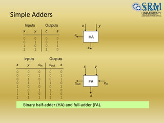
Simple Adders
Binary half-adder(HA) and full-adder (FA).
x y c s
0 0 0 0
0 1 0 1
1 0 0 1
1 1 1 0
Inputs Outputs
HA
x y
c
s
x y c c s
0 0 0 0 0
0 0 1 0 1
0 1 0 0 1
0 1 1 1 0
1 0 0 0 1
1 0 1 1 0
1 1 0 1 0
1 1 1 1 1
Inputs Outputs
cout cin
outin x y
s
FA
32.
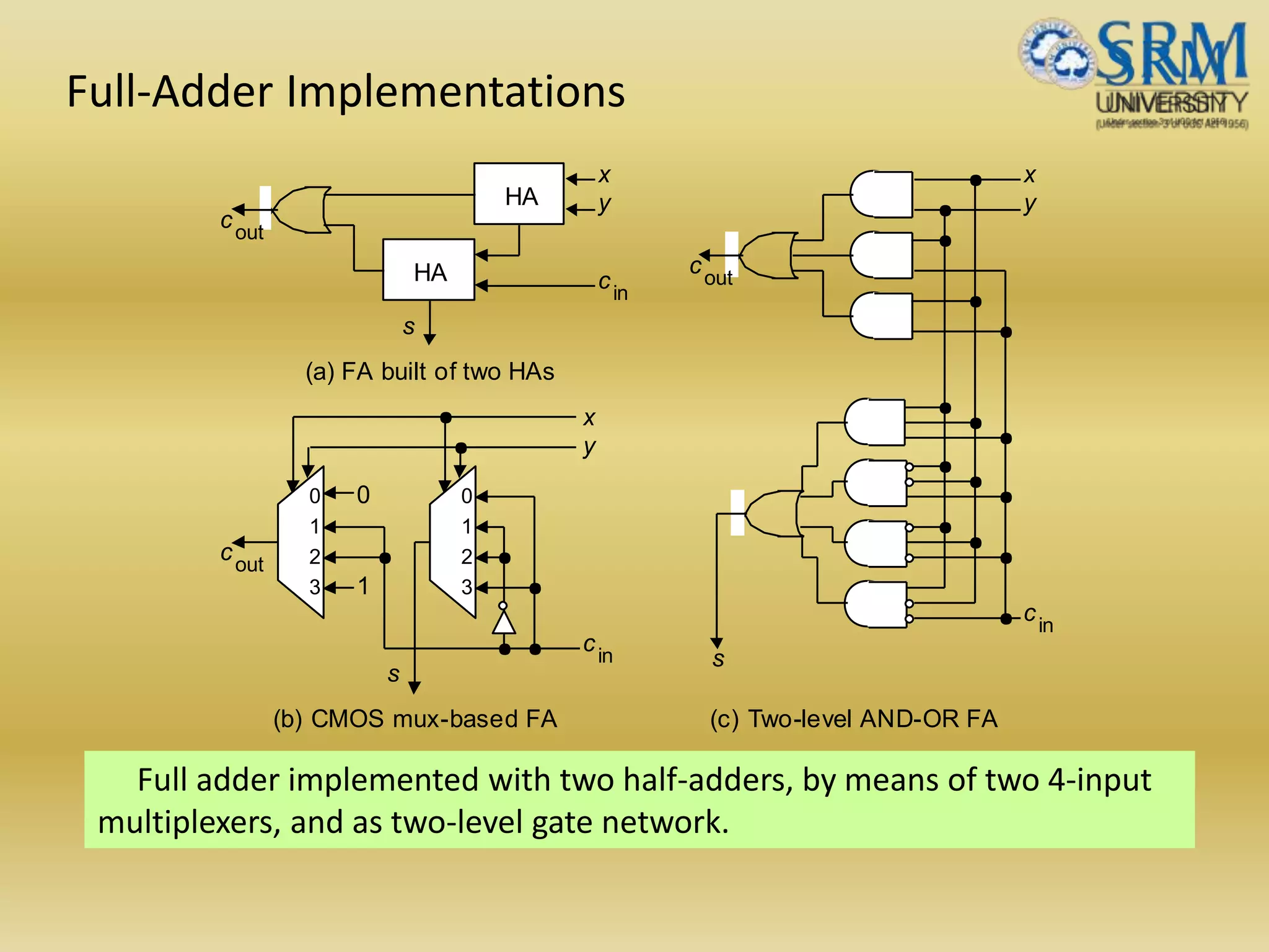
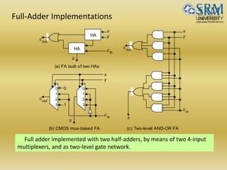
Full-Adder Implementations
Full adderimplemented with two half-adders, by means of two 4-input
multiplexers, and as two-level gate network.
(a) FA built of two HAs
(c) Two-level AND-OR FA(b) CMOS mux-based FA
1
0
3
2
HA
HA
1
0
3
2
0
1
x
y
x
y
x
y
s
s
s
cout
cout
cout
cin
cin
cin
33.
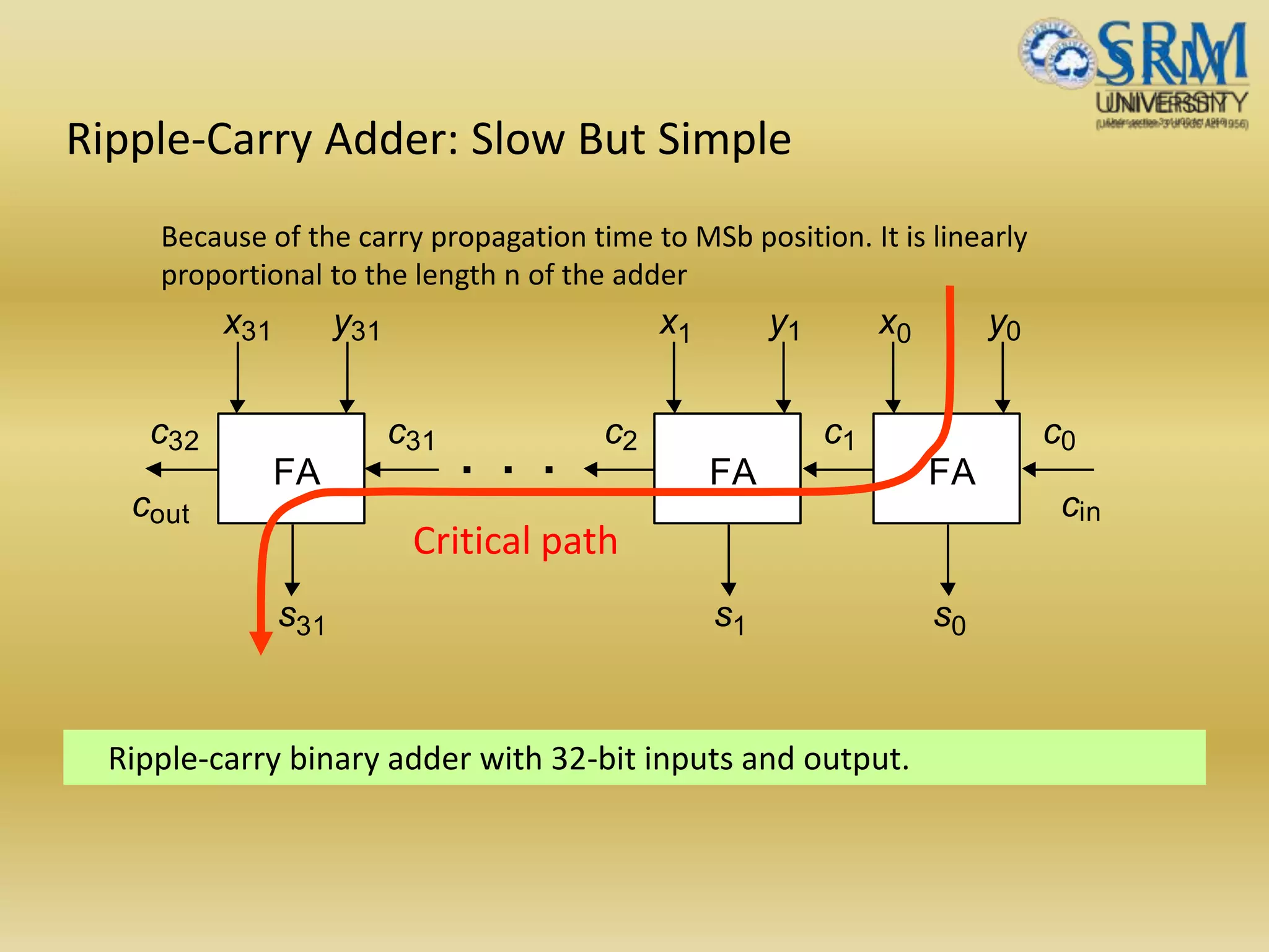
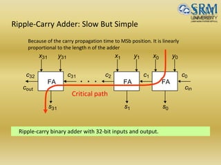
Ripple-Carry Adder: SlowBut Simple
Ripple-carry binary adder with 32-bit inputs and output.
x
s
y
cc
x
s
y
c
x
s
y
c
cout cin
0 0
0
c0
1 1
1
12
31
31
31
31
FA FA FA
32
. . .
Critical path
Because of the carry propagation time to MSb position. It is linearly
proportional to the length n of the adder
34.
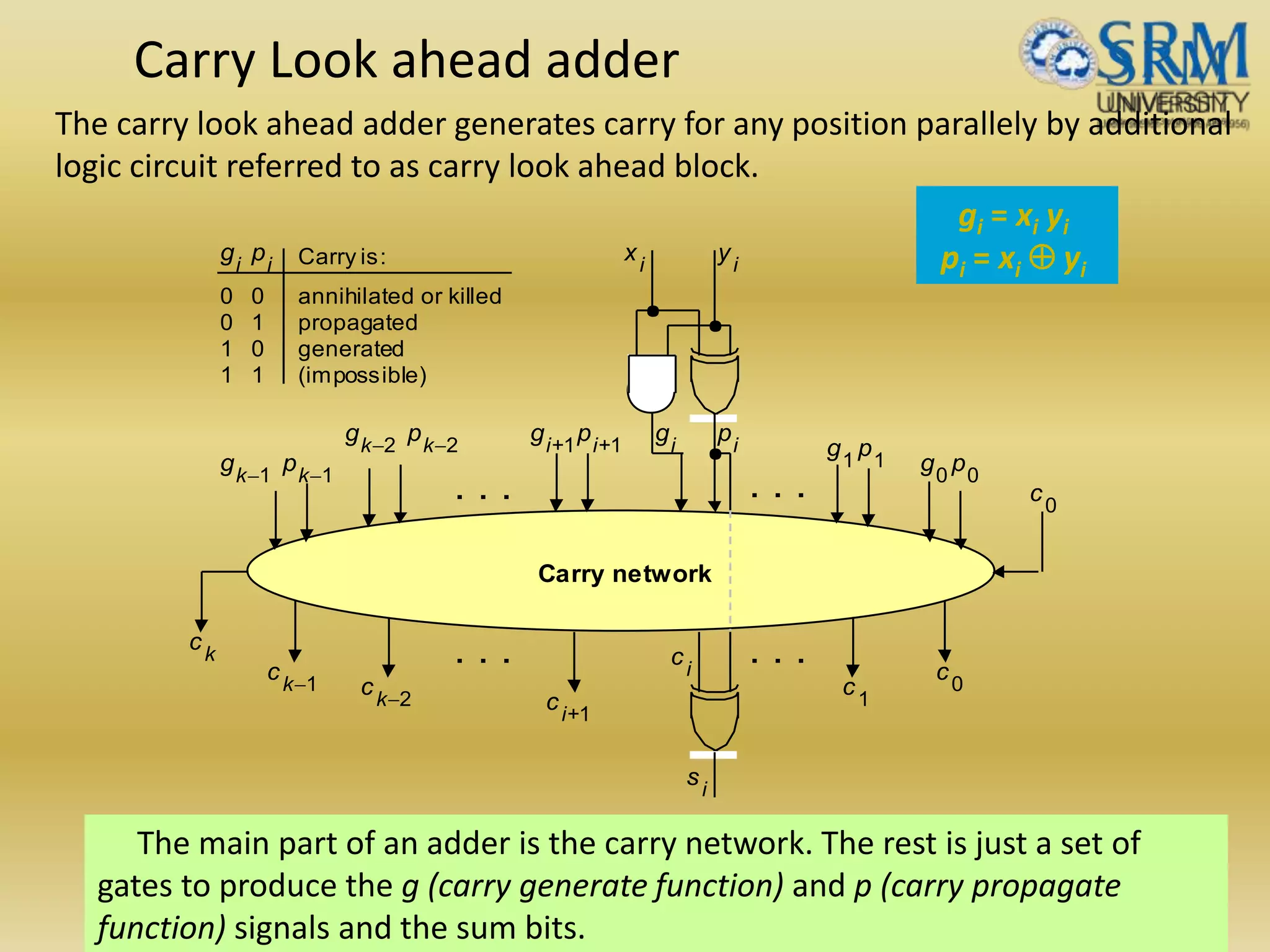
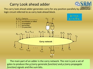
Carry Look aheadadder
The main part of an adder is the carry network. The rest is just a set of
gates to produce the g (carry generate function) and p (carry propagate
function) signals and the sum bits.
Carry network
. . . . . .
xi
yi
g p
s
ii
i
ci
ci+1
ck-1
ck
ck-2
c1
c0
g p11 g p00
g pk-2k-2
g pi+1i+1
g pk-1k-1
c0
. . . . . .
0 0
0 1
1 0
1 1
annihilated or killed
propagated
generated
(impossible)
Carry is:gi
pi
gi = xi yi
pi = xi yi
The carry look ahead adder generates carry for any position parallely by additional
logic circuit referred to as carry look ahead block.
35.
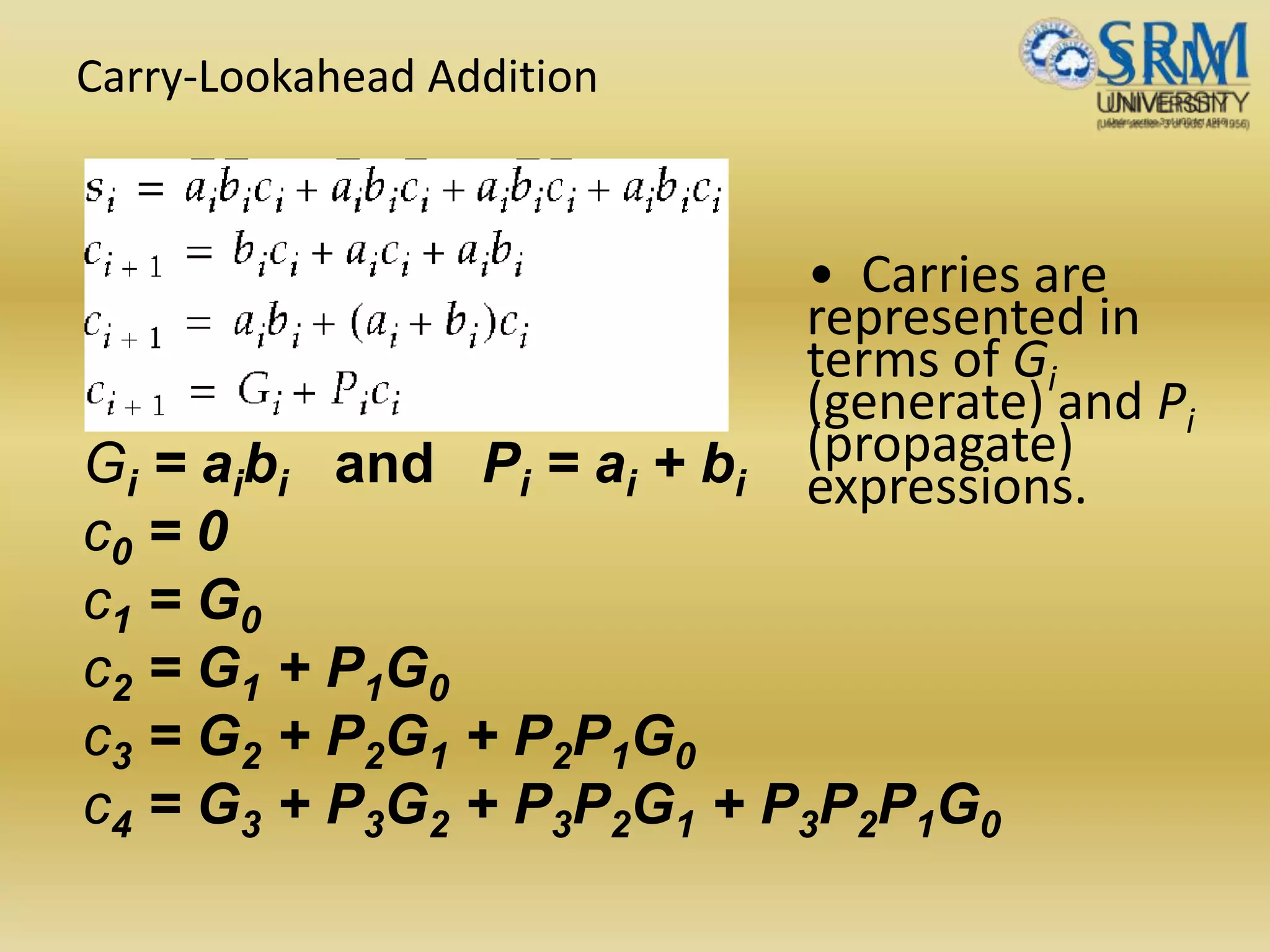
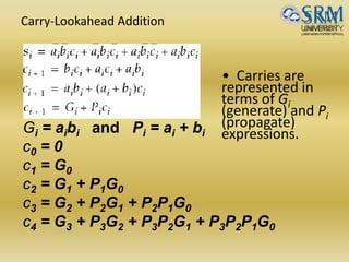
Carry-Lookahead Addition
Gi =aibi and Pi = ai + bi
c0 = 0
c1 = G0
c2 = G1 + P1G0
c3 = G2 + P2G1 + P2P1G0
c4 = G3 + P3G2 + P3P2G1 + P3P2P1G0
• Carries are
represented in
terms of Gi
(generate) and Pi
(propagate)
expressions.
36.
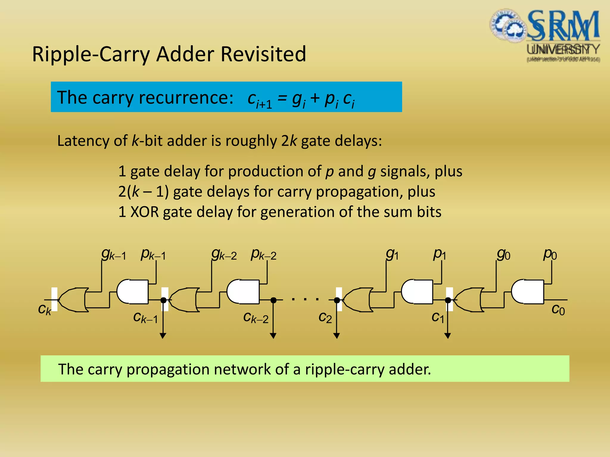
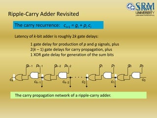
Ripple-Carry Adder Revisited
Thecarry propagation network of a ripple-carry adder.
. . .
ck-1
ck
ck-2 c1
g p11 g p00g pk-2k-2g pk-1k-1
c0
c2
The carry recurrence: ci+1 = gi + pi ci
Latency of k-bit adder is roughly 2k gate delays:
1 gate delay for production of p and g signals, plus
2(k – 1) gate delays for carry propagation, plus
1 XOR gate delay for generation of the sum bits
37.
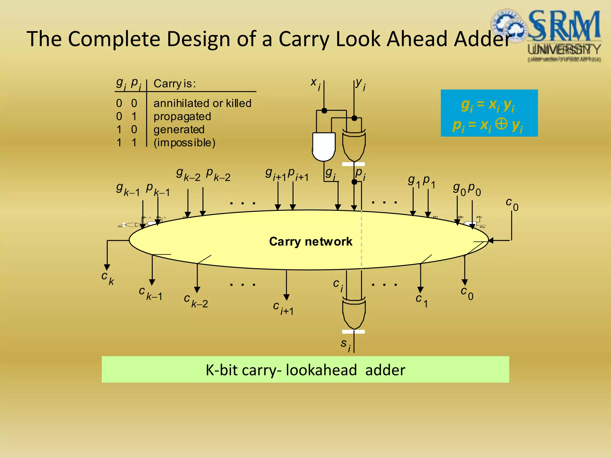
The Complete Designof a Carry Look Ahead Adder
. . .
ck-1
ck
ck-2 c1
g p11 g p00g pk-2k-2g pk-1k-1
c0
c2
. . .
ck-1
ck
ck-2 c1
g p11 g p00g pk-2k-2g pk-1k-1
c0
c2
K-bit carry- lookahead adder
Carry network
. . . . . .
xi
yi
g p
s
ii
i
ci
ci+1
ck-1
ck
ck-2
c1
c0
g p11 g p00
g pk-2k-2
g pi+1i+1
g pk-1k-1
c0
. . . . . .
0 0
0 1
1 0
1 1
annihilated or killed
propagated
generated
(impossible)
Carry is:gi
pi
gi = xi yi
pi = xi yi
38.
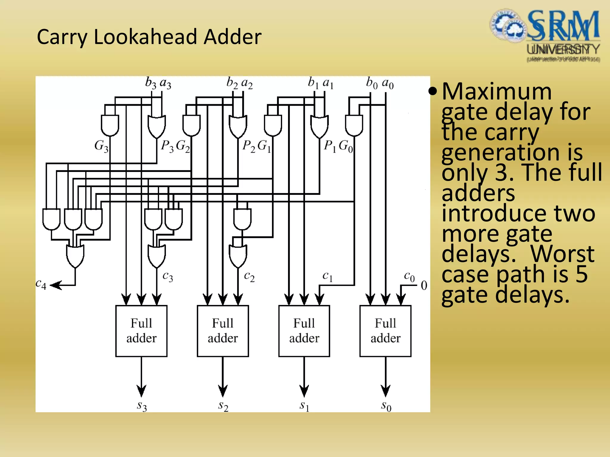
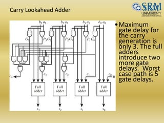
Carry Lookahead Adder
•Maximum
gatedelay for
the carry
generation is
only 3. The full
adders
introduce two
more gate
delays. Worst
case path is 5
gate delays.
39.
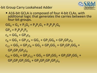
-bit Group CarryLookahead Adder
• A16-bit GCLA is composed of four 4-bit CLAs, with
additional logic that generates the carries between the
four-bit groups.
GG0 = G3 + P3G2 + P3P2G1 + P3P2P1G0
GP0 = P3P2P1P0
c4 = GG0 + GP0c0
c8 = GG1 + GP1c4 = GG1 + GP1GG0 + GP1GP0c0
c12 = GG2 + GP2c8 = GG2 + GP2GG1 + GP2GP1GG0 +
GP2GP1GP0c0
c16 = GG3 + GP3c12 = GG3 + GP3GG2 + GP3GP2GG1 +
GP3GP2GP1GG0 + GP3GP2GP1GP0c0
40.
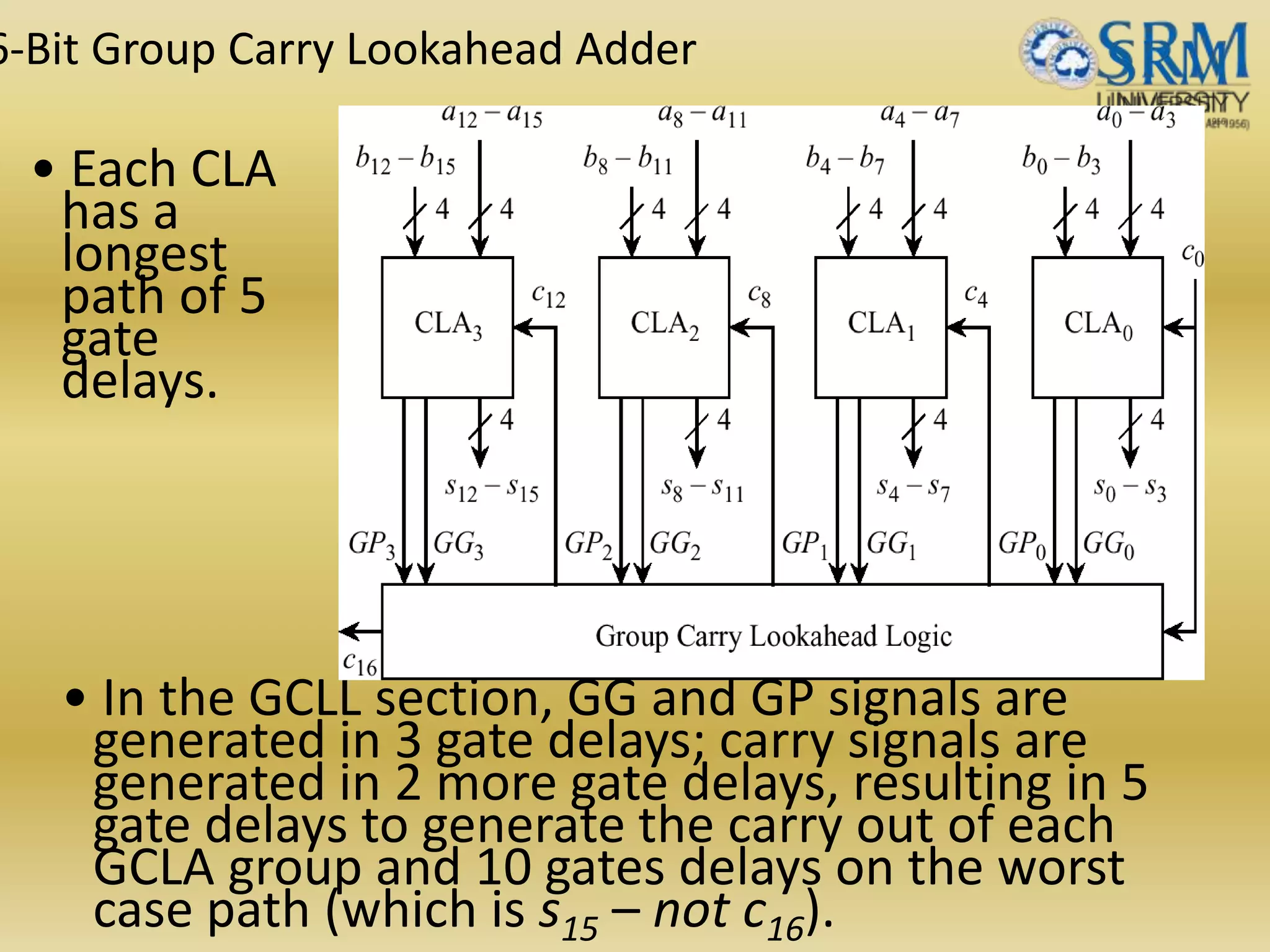
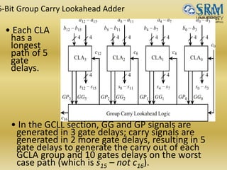
6-Bit Group CarryLookahead Adder
• Each CLA
has a
longest
path of 5
gate
delays.
• In the GCLL section, GG and GP signals are
generated in 3 gate delays; carry signals are
generated in 2 more gate delays, resulting in 5
gate delays to generate the carry out of each
GCLA group and 10 gates delays on the worst
case path (which is s15 – not c16).
41.
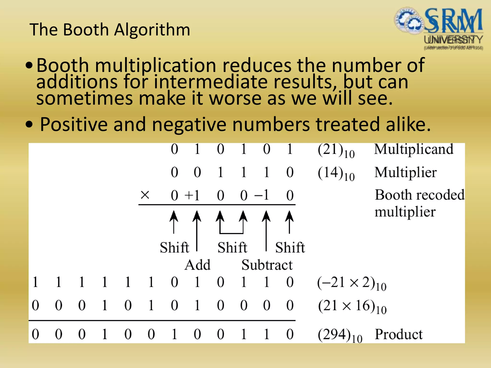
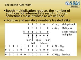
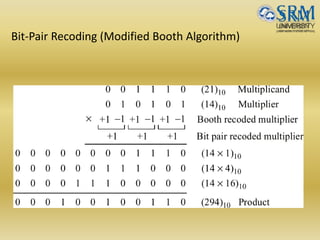
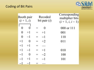
The Booth Algorithm
•Boothmultiplication reduces the number of
additions for intermediate results, but can
sometimes make it worse as we will see.
• Positive and negative numbers treated alike.
42.
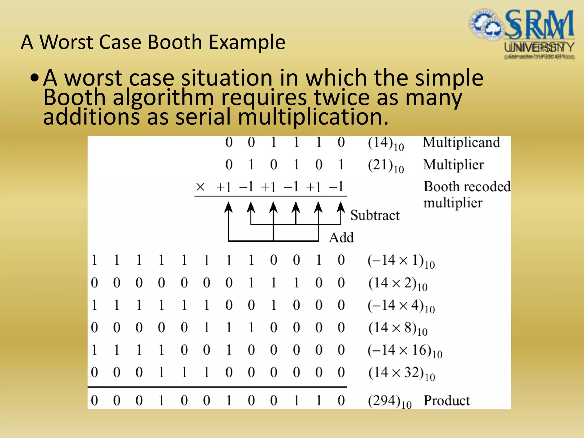
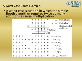
A Worst CaseBooth Example
•A worst case situation in which the simple
Booth algorithm requires twice as many
additions as serial multiplication.
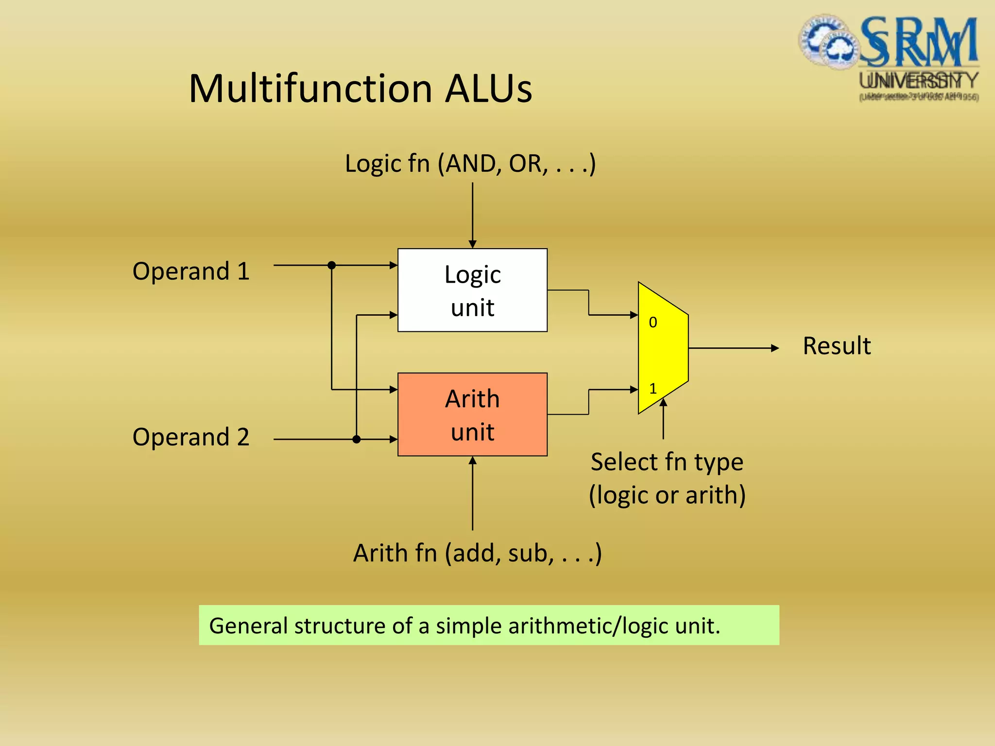
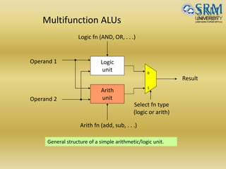
Multifunction ALUs
General structureof a simple arithmetic/logic unit.
Logic
unit
Arith
unit
0
1
Operand 1
Operand 2
Result
Logic fn (AND, OR, . . .)
Arith fn (add, sub, . . .)
Select fn type
(logic or arith)
46.
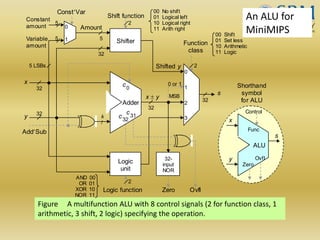
An ALU for
MiniMIPS
FigureA multifunction ALU with 8 control signals (2 for function class, 1
arithmetic, 3 shift, 2 logic) specifying the operation.
AddSub
x y
y
x
Adder
c32
c0
k
/
Shifter
Logic
unit
s
Logic function
Amount
5
2
Constant
amount
Variable
amount
5
5
ConstVar
0
1
0
1
2
3
Function
class
2
Shift function
5 LSBs Shifted y
32
32
32
2
c31
32-
input
NOR
OvflZero
32
32
MSB
ALU
y
x
s
Shorthand
symbol
for ALU
Ovfl
Zero
Func
Control
0 or 1
AND 00
OR 01
XOR 10
NOR 11
00 Shift
01 Set less
10 Arithmetic
11 Logic
00 No shift
01 Logical left
10 Logical right
11 Arith right
47.
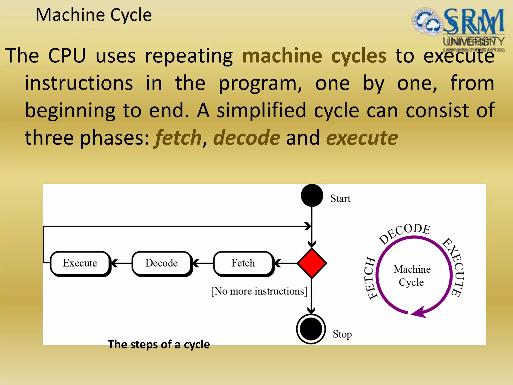
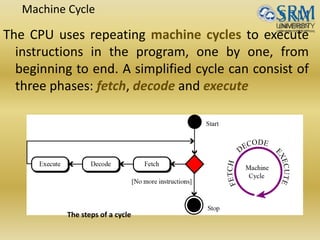
Machine Cycle
The CPUuses repeating machine cycles to execute
instructions in the program, one by one, from
beginning to end. A simplified cycle can consist of
three phases: fetch, decode and execute
The steps of a cycle
48.
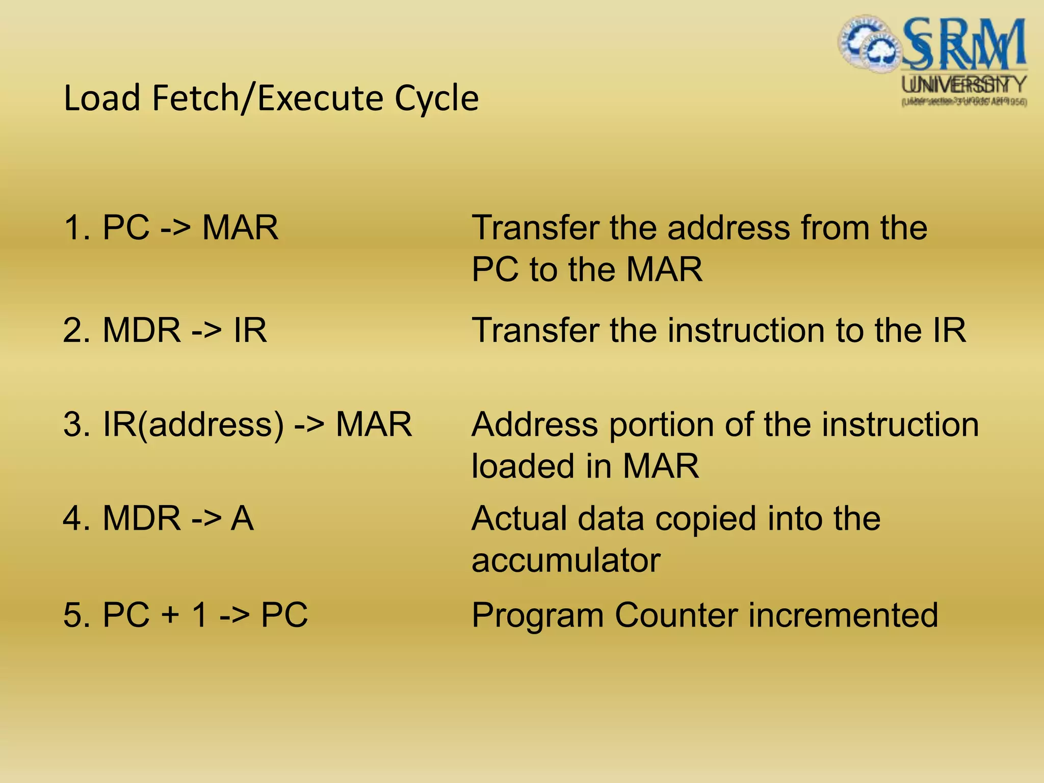
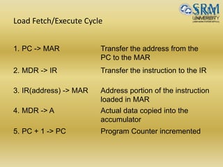
Load Fetch/Execute Cycle
1.PC -> MAR Transfer the address from the
PC to the MAR
2. MDR -> IR Transfer the instruction to the IR
3. IR(address) -> MAR Address portion of the instruction
loaded in MAR
4. MDR -> A Actual data copied into the
accumulator
5. PC + 1 -> PC Program Counter incremented
49.
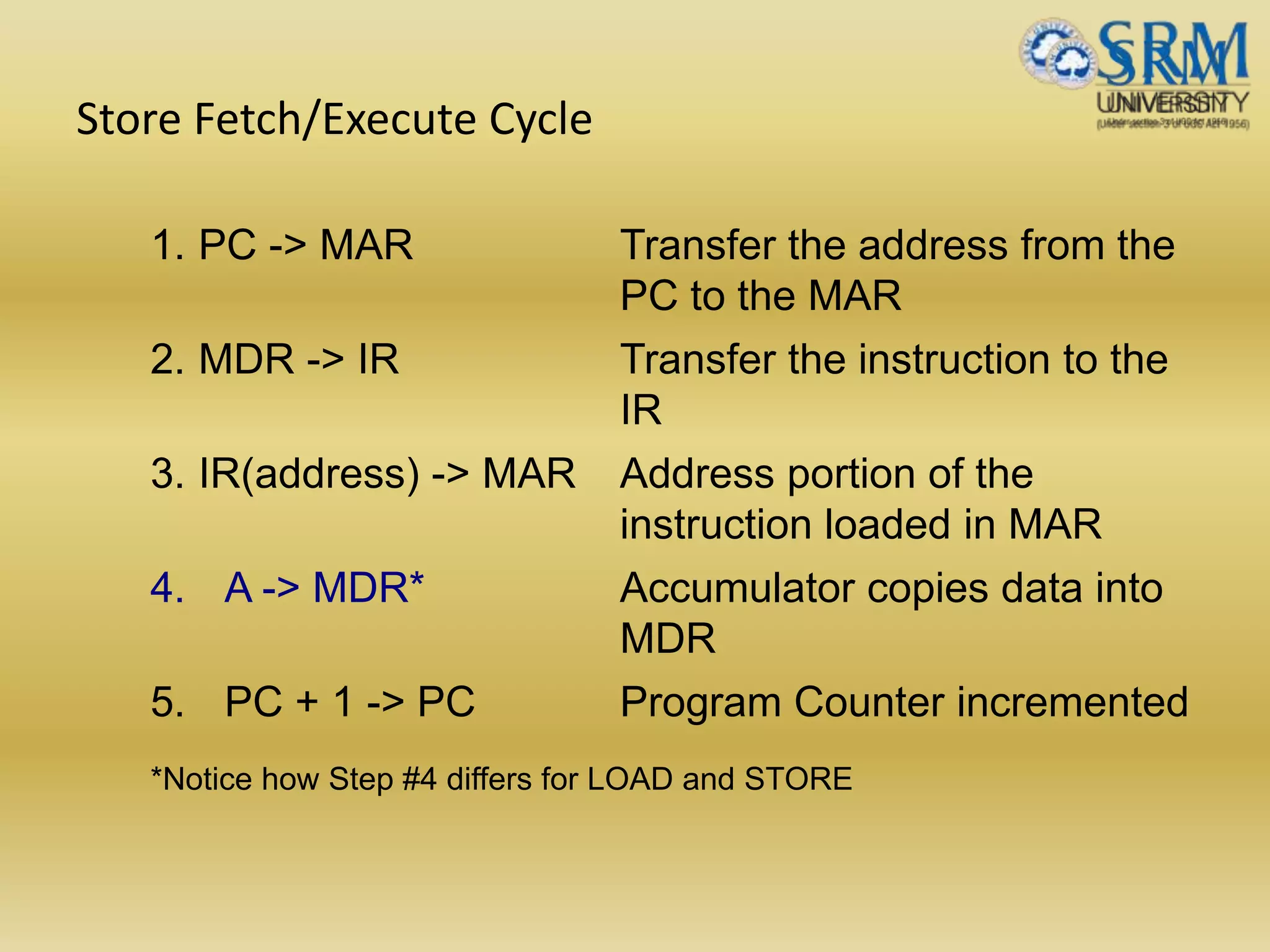
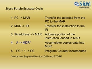
Store Fetch/Execute Cycle
1.PC -> MAR Transfer the address from the
PC to the MAR
2. MDR -> IR Transfer the instruction to the
IR
3. IR(address) -> MAR Address portion of the
instruction loaded in MAR
4. A -> MDR* Accumulator copies data into
MDR
5. PC + 1 -> PC Program Counter incremented
*Notice how Step #4 differs for LOAD and STORE
50.
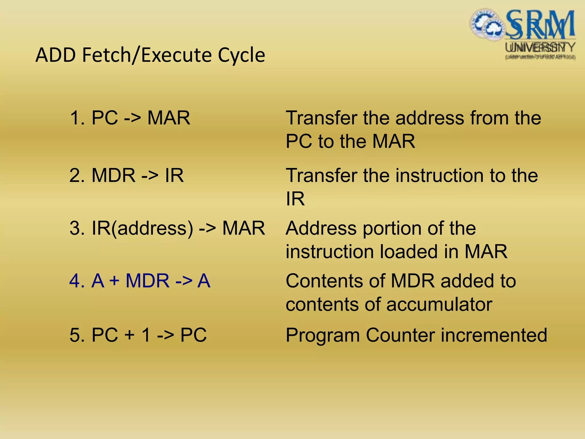
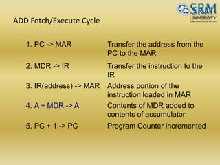
ADD Fetch/Execute Cycle
1.PC -> MAR Transfer the address from the
PC to the MAR
2. MDR -> IR Transfer the instruction to the
IR
3. IR(address) -> MAR Address portion of the
instruction loaded in MAR
4. A + MDR -> A Contents of MDR added to
contents of accumulator
5. PC + 1 -> PC Program Counter incremented
51.
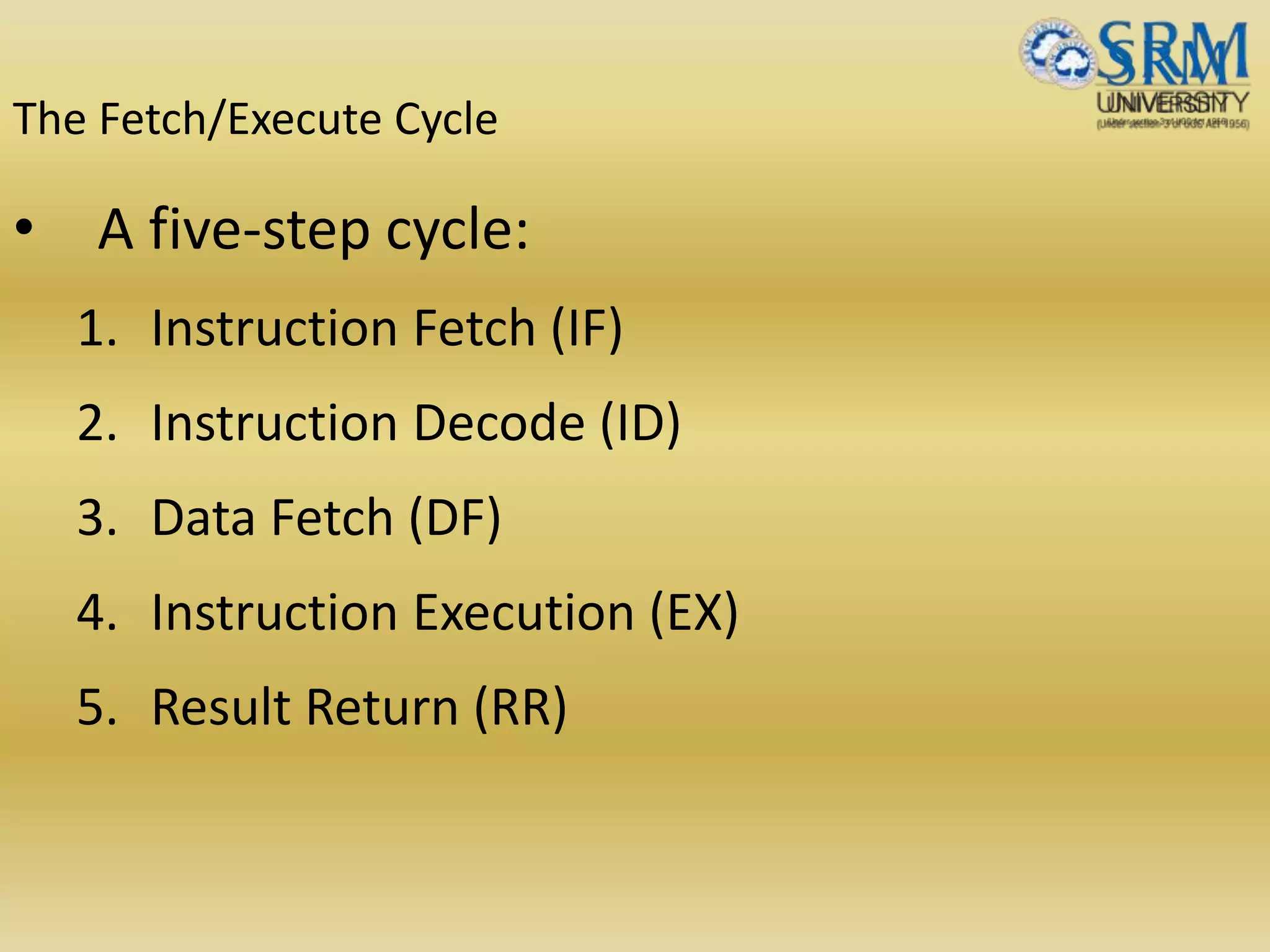
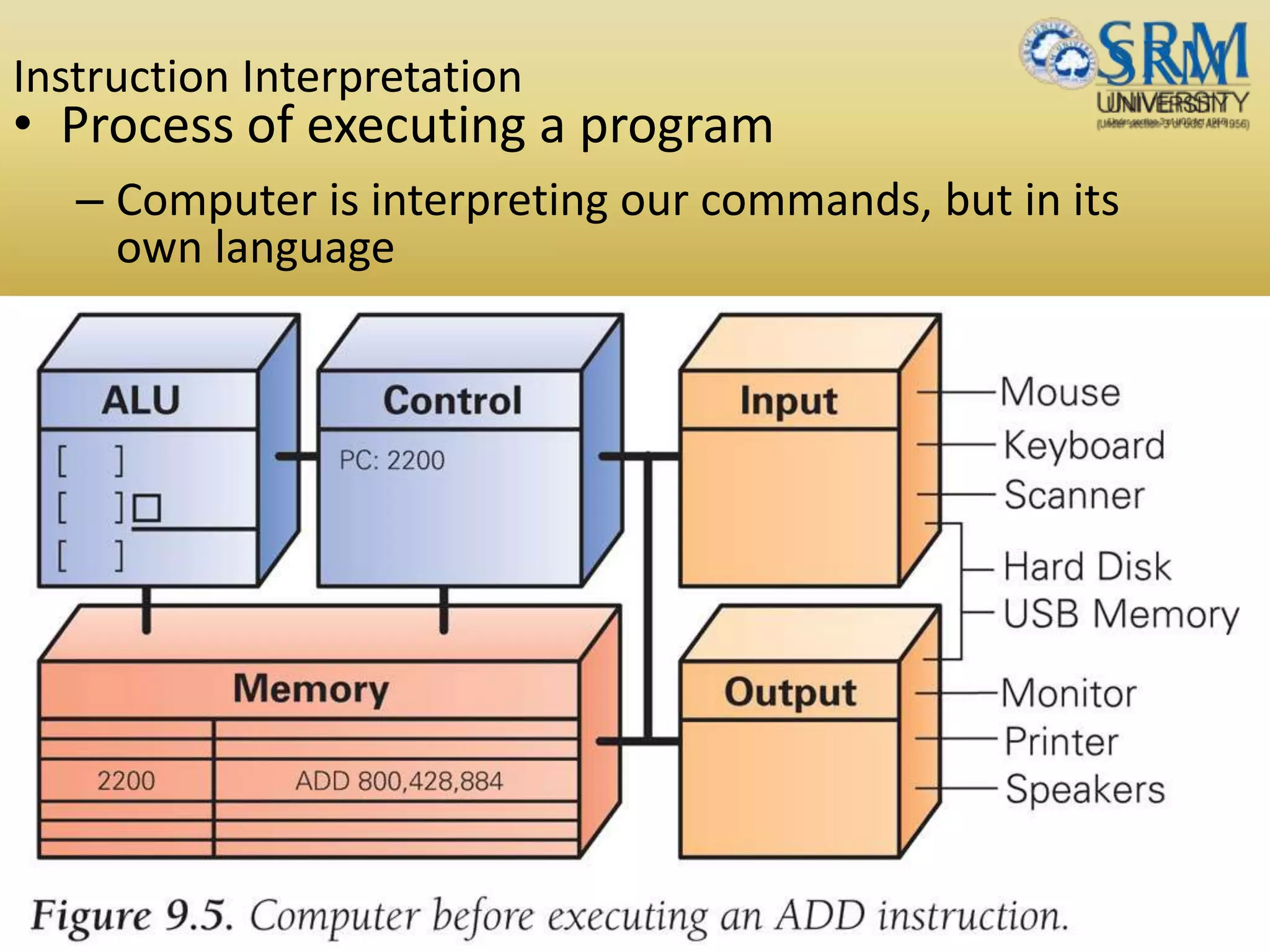
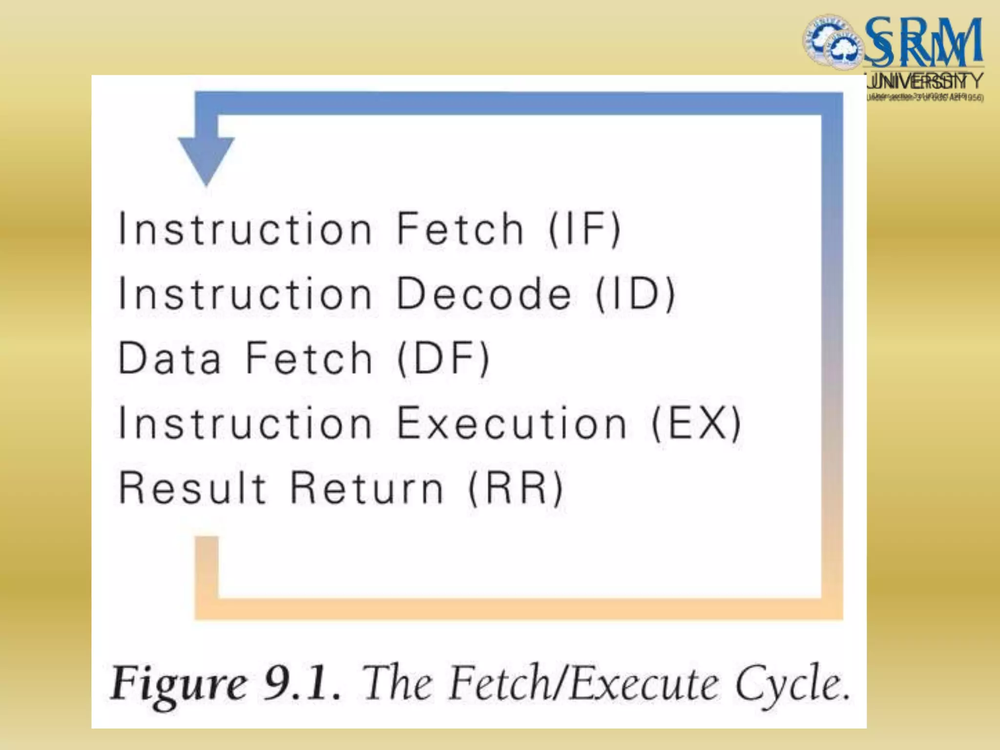
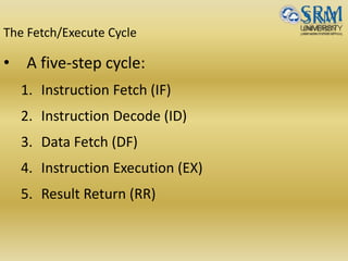
The Fetch/Execute Cycle
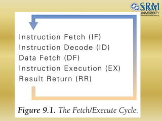
•A five-step cycle:
1. Instruction Fetch (IF)
2. Instruction Decode (ID)
3. Data Fetch (DF)
4. Instruction Execution (EX)
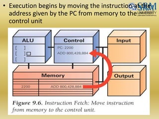
5. Result Return (RR)
• Execution beginsby moving the instruction at the
address given by the PC from memory to the
control unit
54.
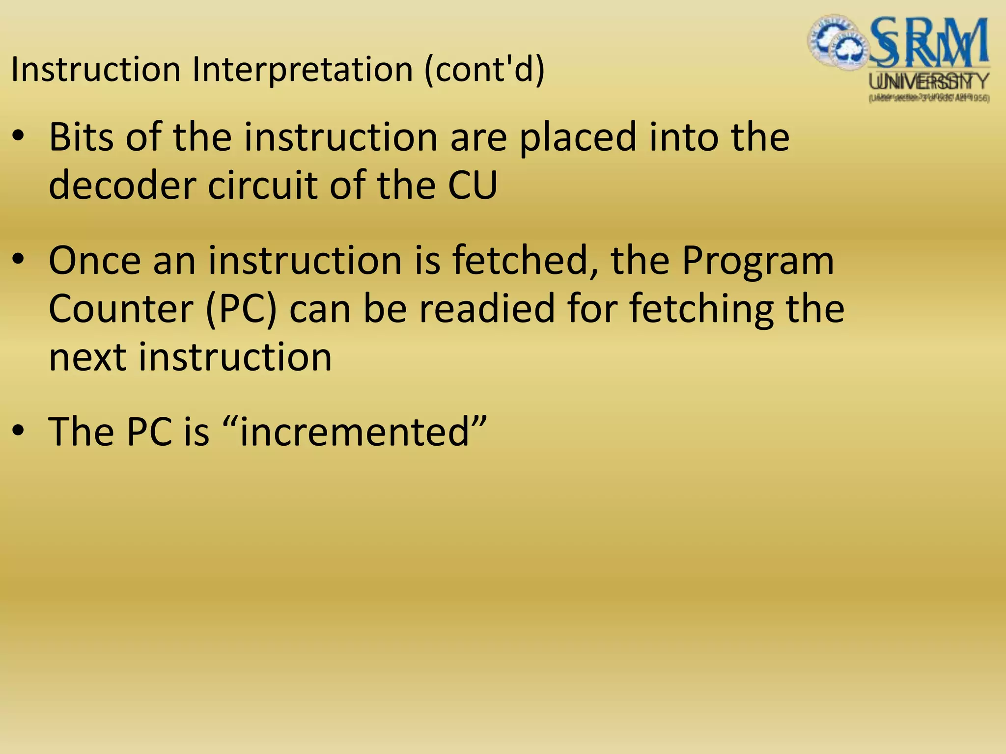
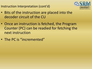
Instruction Interpretation (cont'd)
•Bits of the instruction are placed into the
decoder circuit of the CU
• Once an instruction is fetched, the Program
Counter (PC) can be readied for fetching the
next instruction
• The PC is “incremented”
55.
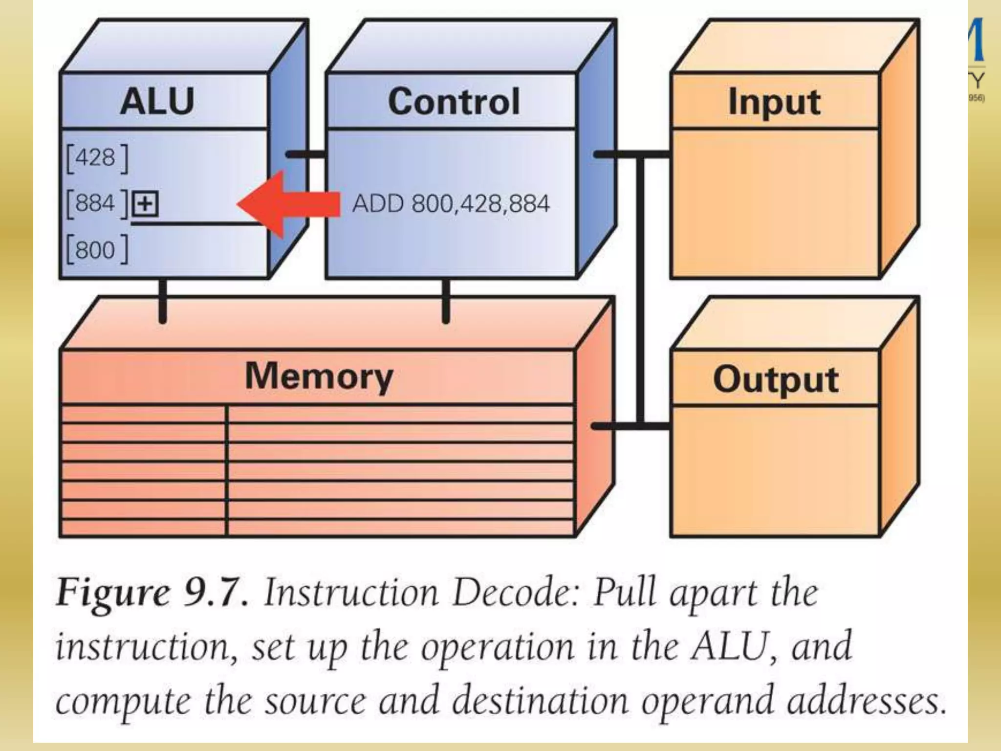
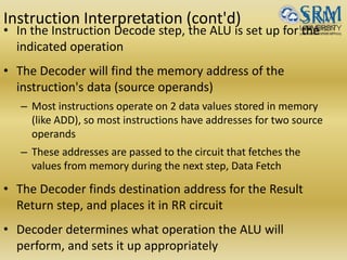
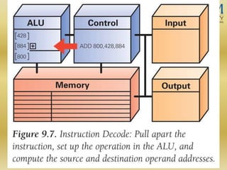
Instruction Interpretation (cont'd)
•In the Instruction Decode step, the ALU is set up for the
indicated operation
• The Decoder will find the memory address of the
instruction's data (source operands)
– Most instructions operate on 2 data values stored in memory
(like ADD), so most instructions have addresses for two source
operands
– These addresses are passed to the circuit that fetches the
values from memory during the next step, Data Fetch
• The Decoder finds destination address for the Result
Return step, and places it in RR circuit
• Decoder determines what operation the ALU will
perform, and sets it up appropriately
58.
Instruction Interpretation
(cont'd)
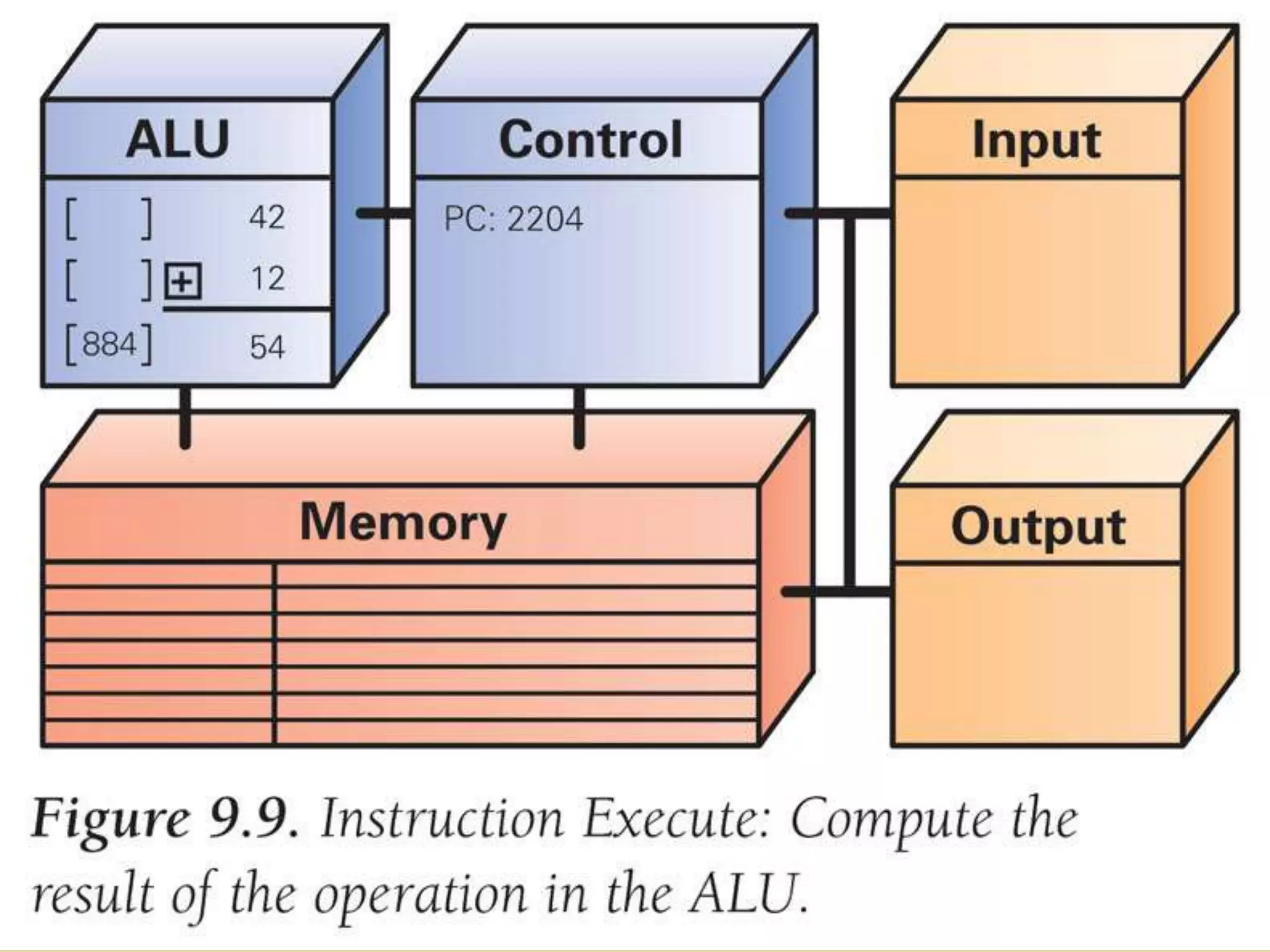
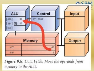
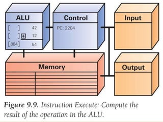
• InstructionExecution: The actual computation
is performed.
• For the ADD instruction, the addition circuit
adds the two source operands together to
produce their sum
60.
Instruction Interpretation
(cont'd)
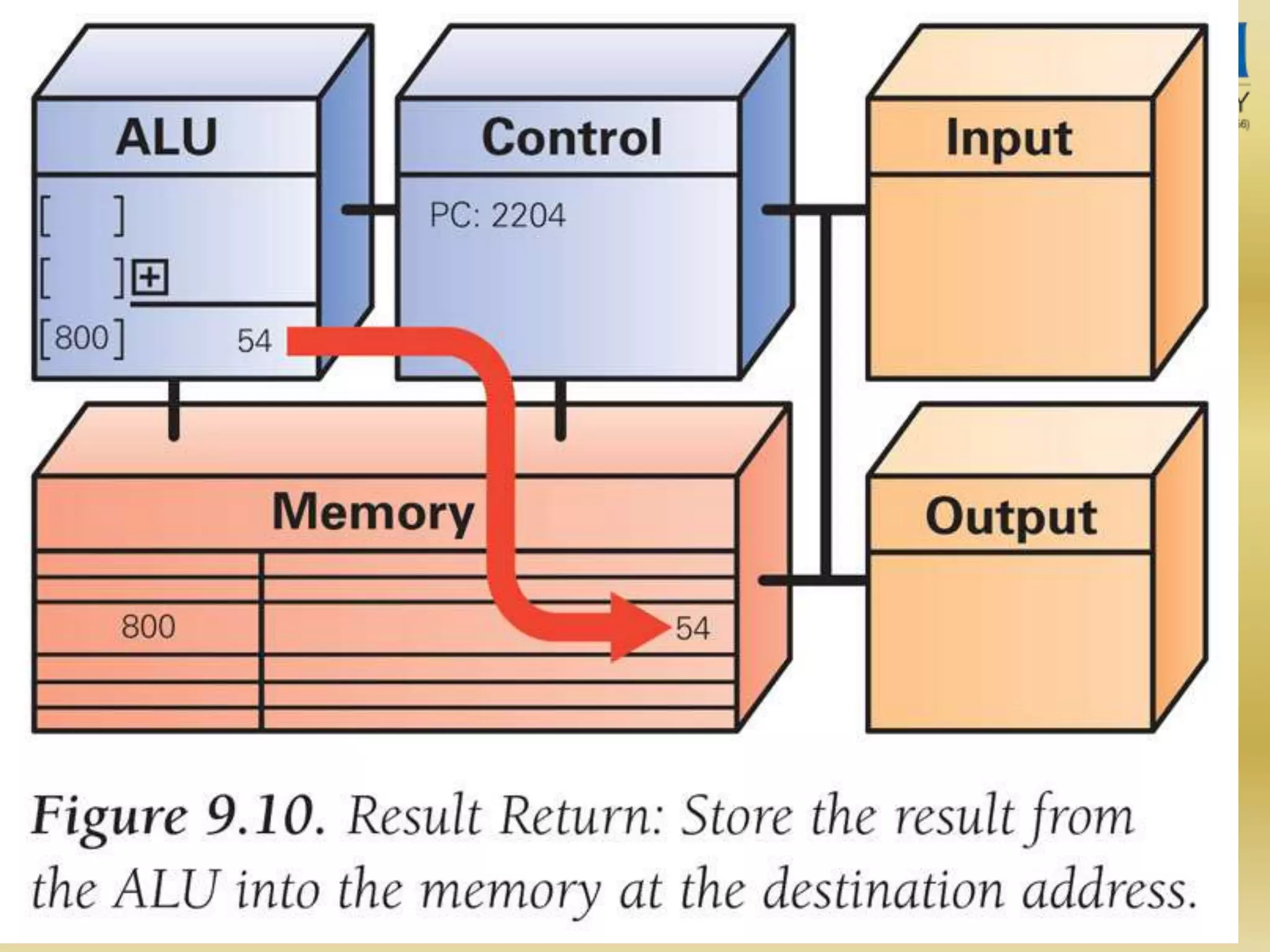
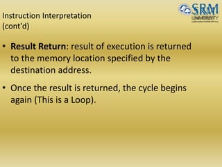
• ResultReturn: result of execution is returned
to the memory location specified by the
destination address.
• Once the result is returned, the cycle begins
again (This is a Loop).
64.
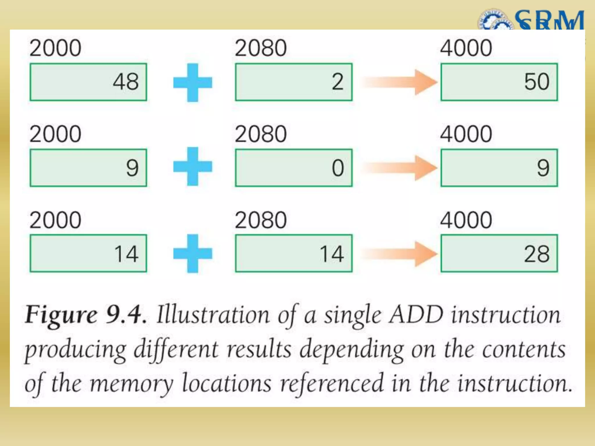
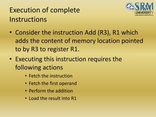
Execution of complete
Instructions
•Consider the instruction Add (R3), R1 which
adds the content of memory location pointed
to by R3 to register R1.
• Executing this instruction requires the
following actions
• Fetch the instruction
• Fetch the first operand
• Perform the addition
• Load the result into R1
65.
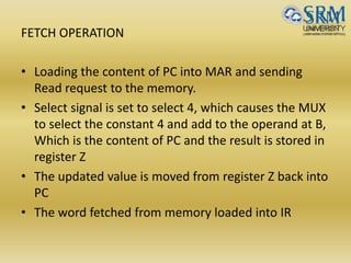
FETCH OPERATION
• Loadingthe content of PC into MAR and sending
Read request to the memory.
• Select signal is set to select 4, which causes the MUX
to select the constant 4 and add to the operand at B,
Which is the content of PC and the result is stored in
register Z
• The updated value is moved from register Z back into
PC
• The word fetched from memory loaded into IR
66.
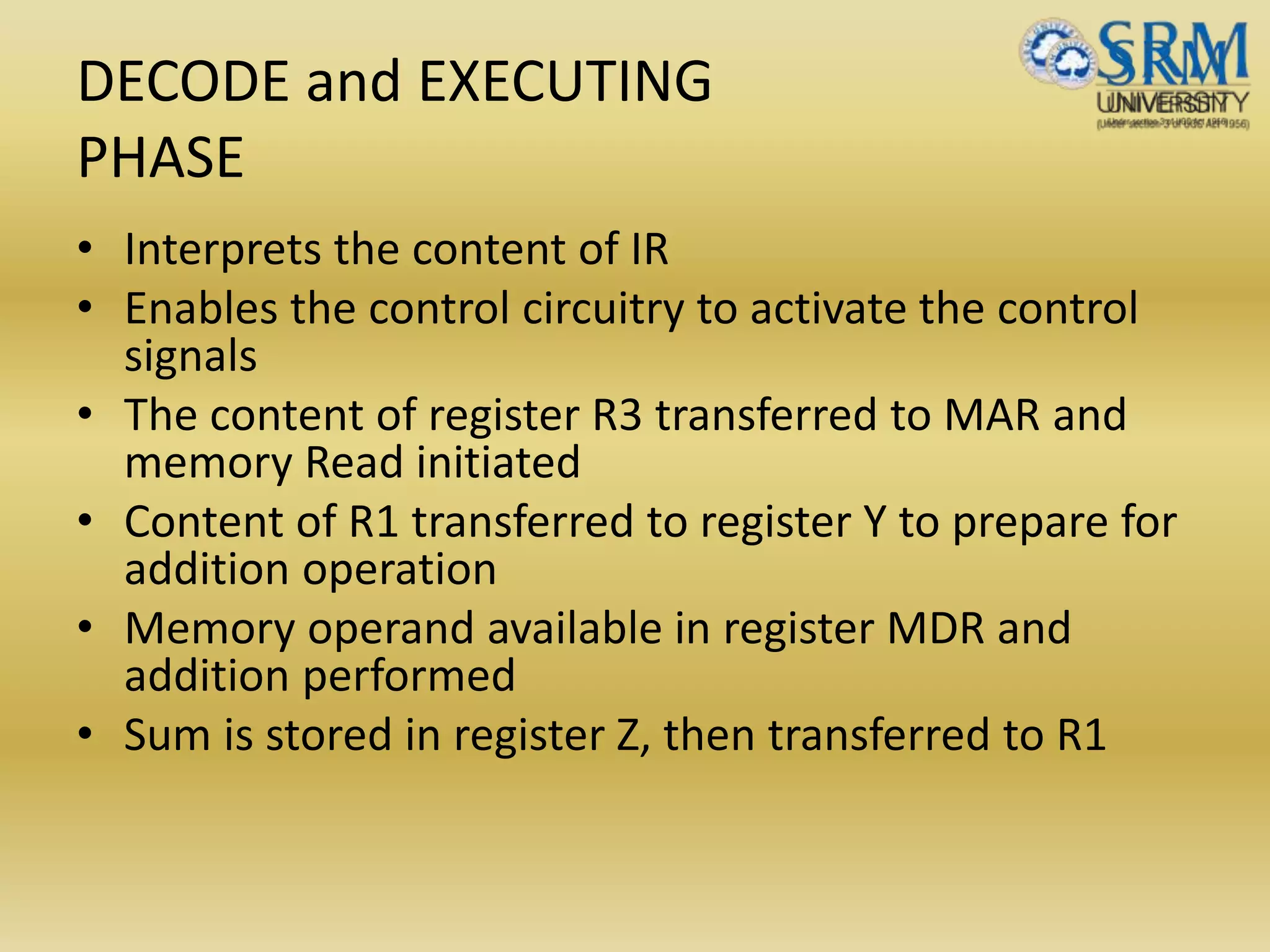
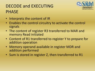
DECODE and EXECUTING
PHASE
•Interprets the content of IR
• Enables the control circuitry to activate the control
signals
• The content of register R3 transferred to MAR and
memory Read initiated
• Content of R1 transferred to register Y to prepare for
addition operation
• Memory operand available in register MDR and
addition performed
• Sum is stored in register Z, then transferred to R1
67.
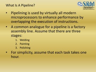
What Is APipeline?
• Pipelining is used by virtually all modern
microprocessors to enhance performance by
overlapping the execution of instructions.
• A common analogue for a pipeline is a factory
assembly line. Assume that there are three
stages:
1. Welding
2. Painting
3. Polishing
• For simplicity, assume that each task takes one
hour.
68.
What Is APipeline?
• If a single person were to work on the product
it would take three hours to produce one
product.
• If we had three people, one person could
work on each stage, upon completing their
stage they could pass their product on to the
next person (since each stage takes one hour
there will be no waiting).
• We could then produce one product per hour
assuming the assembly line has been filled.
69.
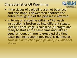
Characteristics Of Pipelining
•If the stages of a pipeline are not balanced
and one stage is slower than another, the
entire throughput of the pipeline is affected.
• In terms of a pipeline within a CPU, each
instruction is broken up into different stages.
Ideally if each stage is balanced (all stages are
ready to start at the same time and take an
equal amount of time to execute.) the time
taken per instruction (pipelined) is defined as:
Time per instruction (unpipelined) / Number of
stages
70.
Characteristics Of Pipelining
•The previous expression is ideal. We will see
later that there are many ways in which a
pipeline cannot function in a perfectly
balanced fashion.
• In terms of a CPU, the implementation of
pipelining has the effect of reducing the
average instruction time, therefore reducing
the average CPI.
• EX: If each instruction in a microprocessor
takes 5 clock cycles (unpipelined) and we have
a 4 stage pipeline, the ideal average CPI with
the pipeline will be 1.25 .
71.
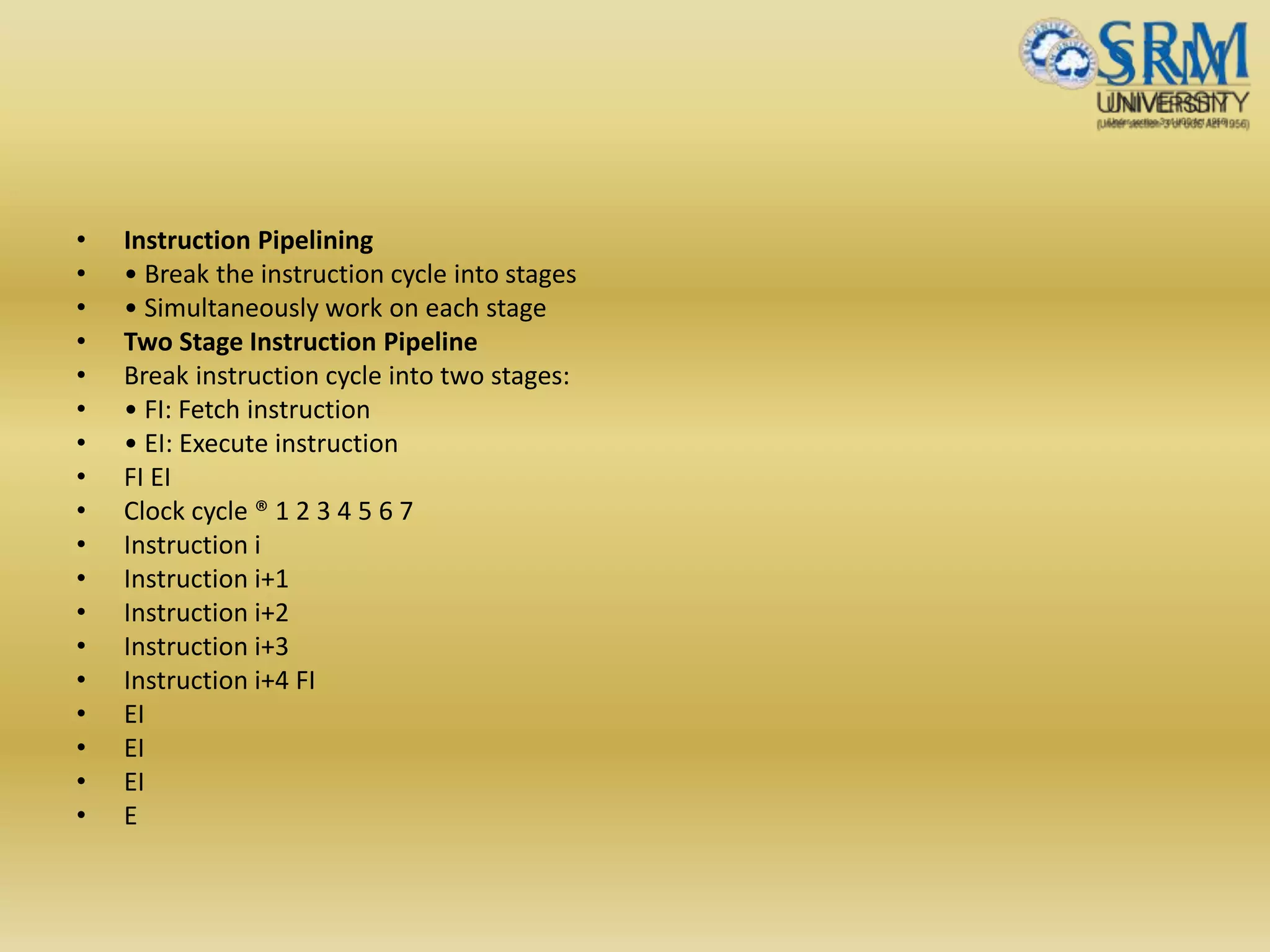
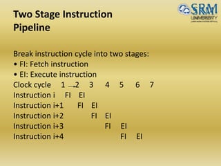
• Instruction Pipelining
•• Break the instruction cycle into stages
• • Simultaneously work on each stage
• Two Stage Instruction Pipeline
• Break instruction cycle into two stages:
• • FI: Fetch instruction
• • EI: Execute instruction
• FI EI
• Clock cycle ® 1 2 3 4 5 6 7
• Instruction i
• Instruction i+1
• Instruction i+2
• Instruction i+3
• Instruction i+4 FI
• EI
• EI
• EI
• E
72.
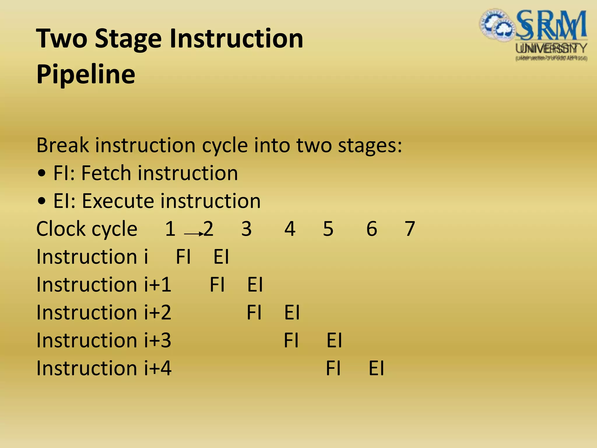
Two Stage Instruction
Pipeline
Breakinstruction cycle into two stages:
• FI: Fetch instruction
• EI: Execute instruction
Clock cycle 1 2 3 4 5 6 7
Instruction i FI EI
Instruction i+1 FI EI
Instruction i+2 FI EI
Instruction i+3 FI EI
Instruction i+4 FI EI
73.
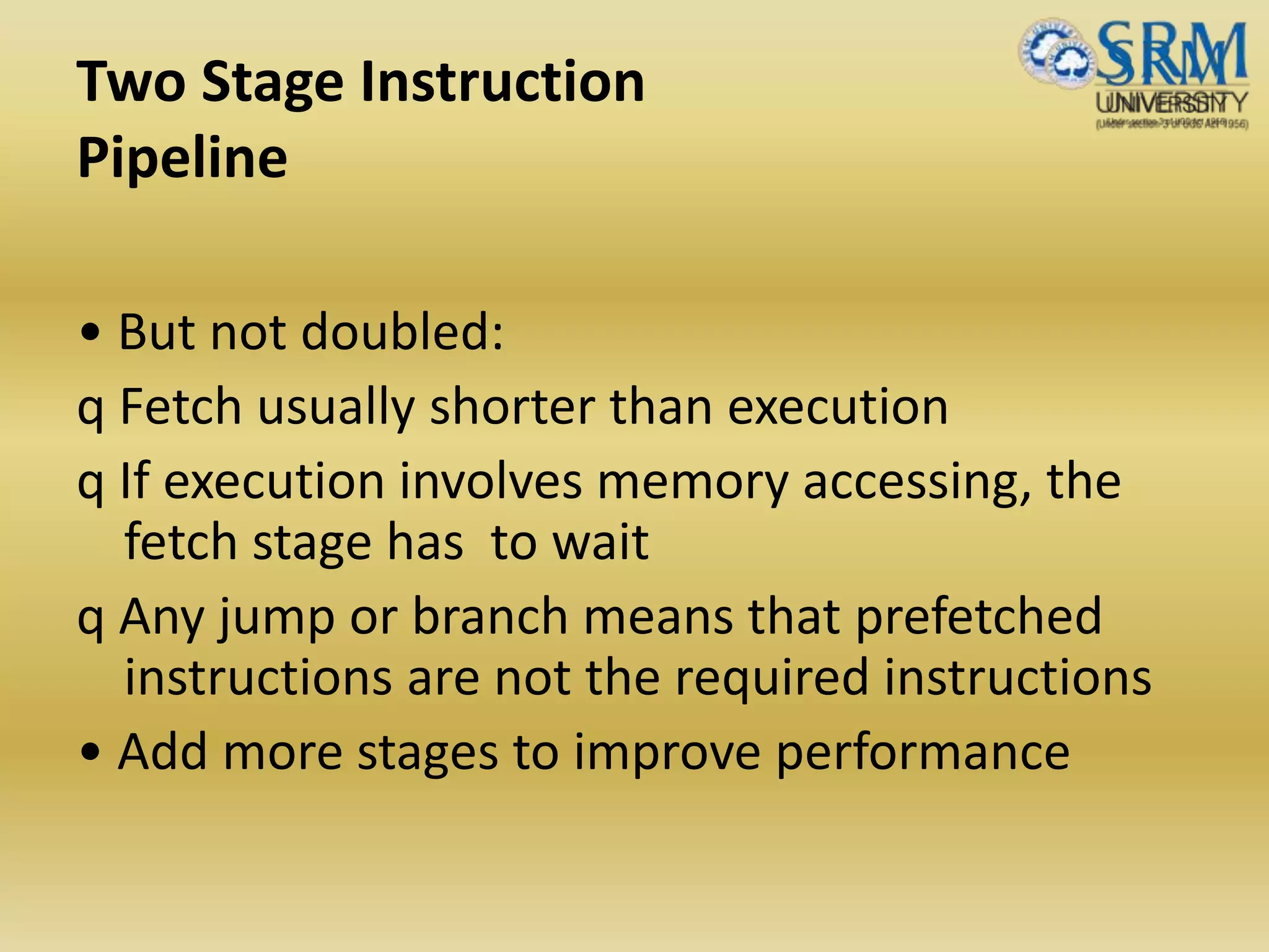
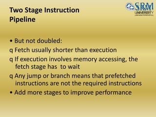
Two Stage Instruction
Pipeline
•But not doubled:
q Fetch usually shorter than execution
q If execution involves memory accessing, the
fetch stage has to wait
q Any jump or branch means that prefetched
instructions are not the required instructions
• Add more stages to improve performance
![Digit Sets and Encodings
Conventional and unconventional digit sets
Decimal digits in [0, 9]; 4-bit BCD, 8-bit ASCII
Hexadecimal, or hex for short: digits 0-9 & a-f
Conventional digit set for radix r is [0, r – 1]
Conventional binary digit set in [0, 1]](https://image.slidesharecdn.com/unitii-170523232217/85/BOOTH-ALGO-DIVISION-RESTORING-_-NON-RESTORING-etc-etc-4-320.jpg)
![Fixed-Point Numbers
Positional representation: k whole and l fractional digits
Value of a number: x = (xk–1xk–2 . . .x1x0 .x–1x–2 . . . x–l )r = S xi r i
For example:
2.375 = (10.011)two = (121) + (020) + (02-1) + (12-2) + (12-3)
Numbers in the range [0, rk – ulp] representable, where ulp = r–l
Fixed-point arithmetic same as integer arithmetic
(radix point implied, not explicit)
Two’s complement properties (including sign change) hold here as well:
(01.011)2’s-compl = (–021) + (120) + (02–1) + (12–2) + (12–3) = +1.375
(11.011)2’s-compl = (–121) + (120) + (02–1) + (12–2) + (12–3) = –0.625](https://image.slidesharecdn.com/unitii-170523232217/85/BOOTH-ALGO-DIVISION-RESTORING-_-NON-RESTORING-etc-etc-7-320.jpg)

![Unsigned Binary Integers
Schematic representation of 4-bit code for integers in [0,
15].
0000
00011111
00101110
00111101
01001100
1000
01011011
01101010
01111001
0
1
2
3
4
5
6
7
15
11
14
13
12
8
9
10
Inside: Natural number
Outside: 4-bit encoding
0
1
2
3
15
4
5
6
789
Turn x notches
counterclockwise
to add x
Turn y notches
clockwise
to subtract y
11
14
13
12
10](https://image.slidesharecdn.com/unitii-170523232217/85/BOOTH-ALGO-DIVISION-RESTORING-_-NON-RESTORING-etc-etc-9-320.jpg)

![Floating-point Computations
• Representation: (fraction, exponent) Has three fields:
sign, significant digits and exponent
eg.111101.100110 1.11101100110*25
• Value representation = +/- M*2 E’-127
In case of a 32 bit number 1 bit represents sign
8 bits represents exponent E’=E +127(bias) [ excess 127
format]
23 bits represents Mantissa](https://image.slidesharecdn.com/unitii-170523232217/85/BOOTH-ALGO-DIVISION-RESTORING-_-NON-RESTORING-etc-etc-19-320.jpg)
![Short and Long IEEE 754 Formats: Features
Table Some features of ANSI/IEEE standard floating-point formats
Feature Single/Short Double/Long
Word width in bits 32 64
Significand in bits 23 + 1 hidden 52 + 1 hidden
Significand range [1, 2 – 2–23] [1, 2 – 2–52]
Exponent bits 8 11
Exponent bias 127 1023
Zero (±0) e + bias = 0, f = 0 e + bias = 0, f = 0
Denormal e + bias = 0, f ≠ 0
represents ±0.f 2–126
e + bias = 0, f ≠ 0
represents ±0.f 2–1022
Infinity (∞) e + bias = 255, f = 0 e + bias = 2047, f = 0
Not-a-number (NaN) e + bias = 255, f ≠ 0 e + bias = 2047, f ≠ 0
Ordinary number e + bias [1, 254]
e [–126, 127]
represents 1.f 2e
e + bias [1, 2046]
e [–1022, 1023]
represents 1.f 2e
min 2–126 1.2 10–38 2–1022 2.2 10–308
max 2128 3.4 1038 21024 1.8 10308](https://image.slidesharecdn.com/unitii-170523232217/85/BOOTH-ALGO-DIVISION-RESTORING-_-NON-RESTORING-etc-etc-25-320.jpg)


![Digit Sets and Encodings
Conventional and unconventional digit sets
Decimal digits in [0, 9]; 4-bit BCD, 8-bit ASCII
Hexadecimal, or hex for short: digits 0-9 & a-f
Conventional digit set for radix r is [0, r – 1]
Conventional binary digit set in [0, 1]](https://image.slidesharecdn.com/unitii-170523232217/75/BOOTH-ALGO-DIVISION-RESTORING-_-NON-RESTORING-etc-etc-4-2048.jpg)
![Fixed-Point Numbers
Positional representation: k whole and l fractional digits
Value of a number: x = (xk–1xk–2 . . .x1x0 .x–1x–2 . . . x–l )r = S xi r i
For example:
2.375 = (10.011)two = (121) + (020) + (02-1) + (12-2) + (12-3)
Numbers in the range [0, rk – ulp] representable, where ulp = r–l
Fixed-point arithmetic same as integer arithmetic
(radix point implied, not explicit)
Two’s complement properties (including sign change) hold here as well:
(01.011)2’s-compl = (–021) + (120) + (02–1) + (12–2) + (12–3) = +1.375
(11.011)2’s-compl = (–121) + (120) + (02–1) + (12–2) + (12–3) = –0.625](https://image.slidesharecdn.com/unitii-170523232217/75/BOOTH-ALGO-DIVISION-RESTORING-_-NON-RESTORING-etc-etc-7-2048.jpg)
![Unsigned Binary Integers
Schematic representation of 4-bit code for integers in [0,
15].
0000
00011111
00101110
00111101
01001100
1000
01011011
01101010
01111001
0
1
2
3
4
5
6
7
15
11
14
13
12
8
9
10
Inside: Natural number
Outside: 4-bit encoding
0
1
2
3
15
4
5
6
789
Turn x notches
counterclockwise
to add x
Turn y notches
clockwise
to subtract y
11
14
13
12
10](https://image.slidesharecdn.com/unitii-170523232217/75/BOOTH-ALGO-DIVISION-RESTORING-_-NON-RESTORING-etc-etc-9-2048.jpg)
![Floating-point Computations
• Representation: (fraction, exponent) Has three fields:
sign, significant digits and exponent
eg.111101.100110 1.11101100110*25
• Value representation = +/- M*2 E’-127
In case of a 32 bit number 1 bit represents sign
8 bits represents exponent E’=E +127(bias) [ excess 127
format]
23 bits represents Mantissa](https://image.slidesharecdn.com/unitii-170523232217/75/BOOTH-ALGO-DIVISION-RESTORING-_-NON-RESTORING-etc-etc-19-2048.jpg)
![Short and Long IEEE 754 Formats: Features
Table Some features of ANSI/IEEE standard floating-point formats
Feature Single/Short Double/Long
Word width in bits 32 64
Significand in bits 23 + 1 hidden 52 + 1 hidden
Significand range [1, 2 – 2–23] [1, 2 – 2–52]
Exponent bits 8 11
Exponent bias 127 1023
Zero (±0) e + bias = 0, f = 0 e + bias = 0, f = 0
Denormal e + bias = 0, f ≠ 0
represents ±0.f 2–126
e + bias = 0, f ≠ 0
represents ±0.f 2–1022
Infinity (∞) e + bias = 255, f = 0 e + bias = 2047, f = 0
Not-a-number (NaN) e + bias = 255, f ≠ 0 e + bias = 2047, f ≠ 0
Ordinary number e + bias [1, 254]
e [–126, 127]
represents 1.f 2e
e + bias [1, 2046]
e [–1022, 1023]
represents 1.f 2e
min 2–126 1.2 10–38 2–1022 2.2 10–308
max 2128 3.4 1038 21024 1.8 10308](https://image.slidesharecdn.com/unitii-170523232217/75/BOOTH-ALGO-DIVISION-RESTORING-_-NON-RESTORING-etc-etc-25-2048.jpg)