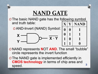
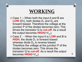
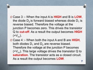
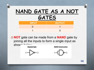
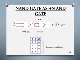
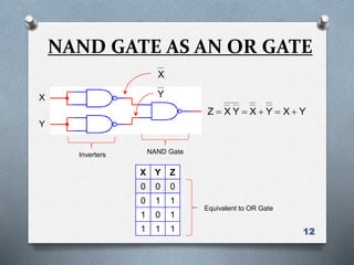
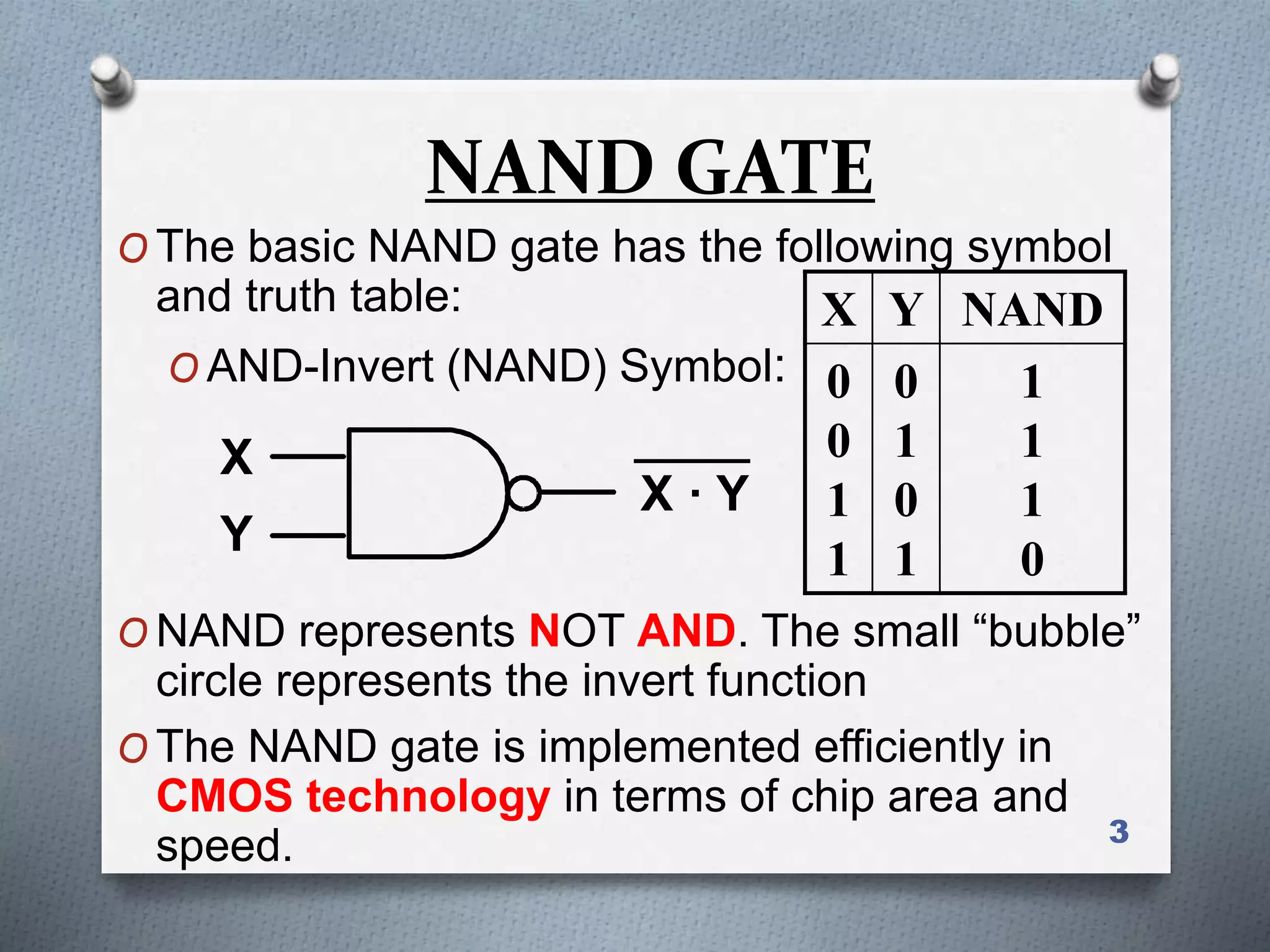
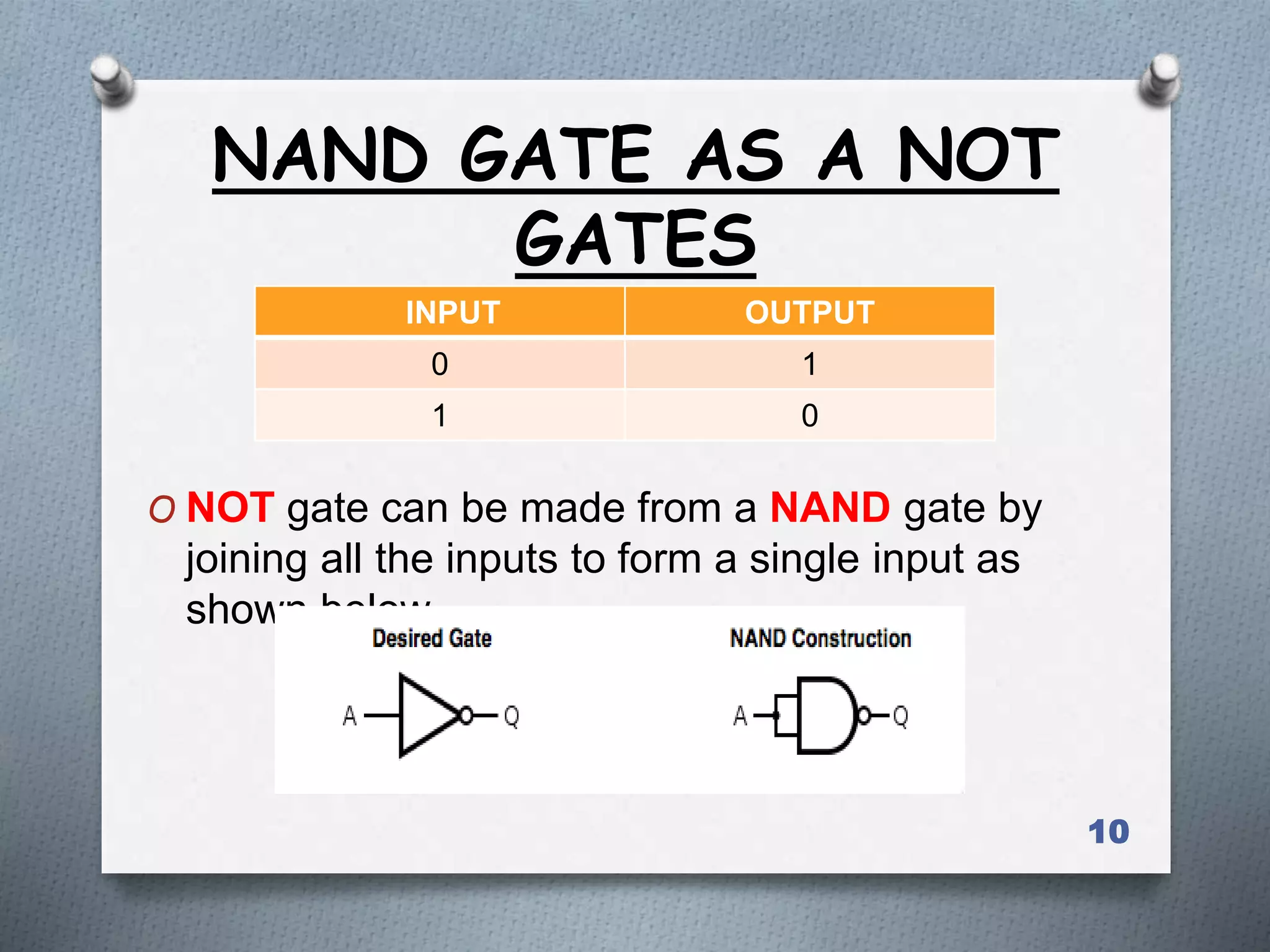
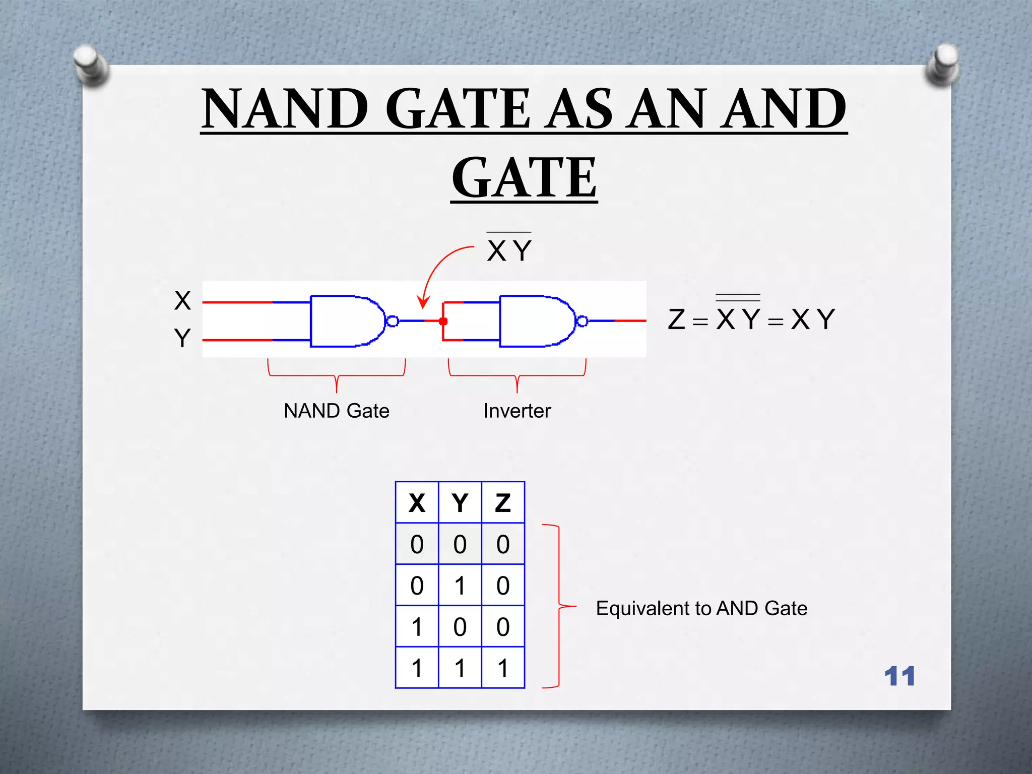
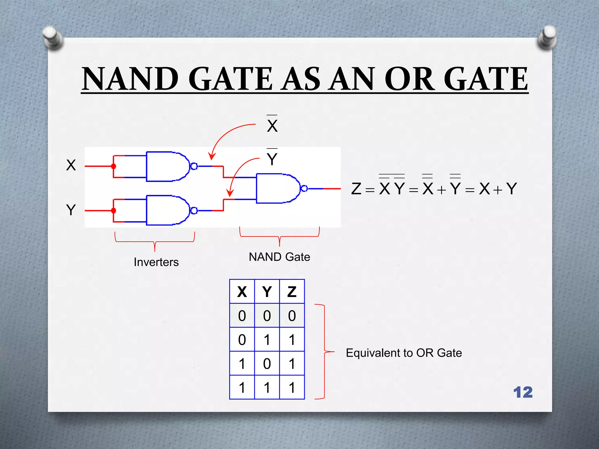
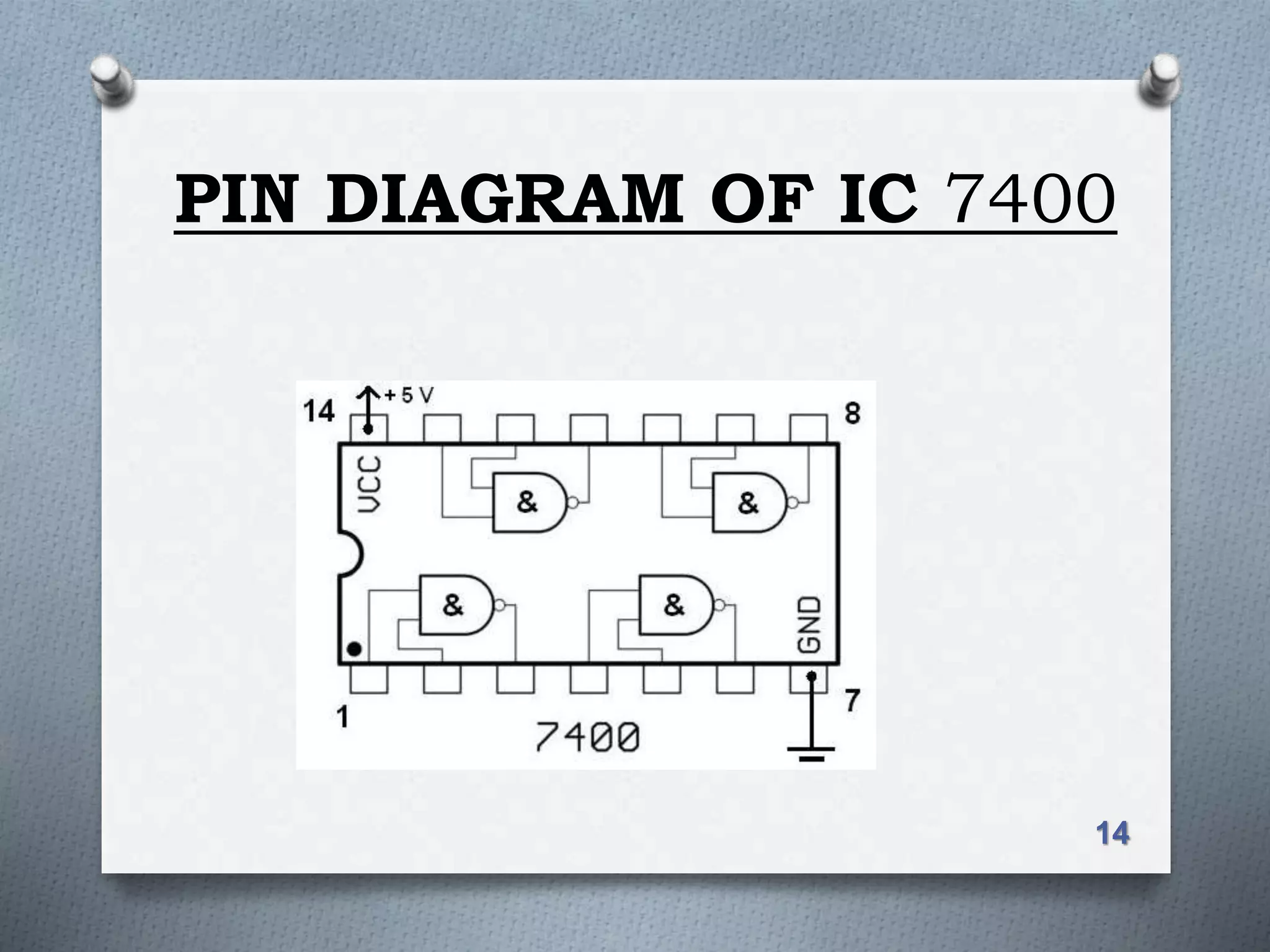
KEMBAR78
NAND gate | PPTX
1
DTL – DIODE TRANSISTOR
LOGIC NAND GATE
O NAND gate is a electronic circuit which has
two or more inputs but only one output.
O The NAND gate is the natural implementation
for the simplest and fastest electronic circuits
O The output is HIGH if at least one of its input
is LOW.
O The output is LOW only when all the inputs
are HIGH.
O The term NAND is a contraction of NOT-AND.
O The NAND gate is a combination of an AND
gate followed by NOT gate.
2
3
NAND GATE
O The basic NAND gate has the following symbol
and truth table:
O AND-Invert (NAND) Symbol:
O NAND represents NOT AND. The small “bubble”
circle represents the invert function
O The NAND gate is implemented efficiently in
CMOS technology in terms of chip area and
speed.
X
Y
X · Y
X Y NAND
0
0
1
1
0
1
0
1
1
1
1
0
4
COMPONENTS USED
5
RESISTOR
DIODE
(1n4002)
TRANSISTOR(BC107)
6
O BREADBOARD
O WIRES
WORKING
O Case 1 :- When both the input A and B are
LOW (0V), both diodes D1 and D2 are
forward biased. Therefore the voltage at the
junction P of the diodes becomes zero. This
drives the transistor Q to cut-off. As a result
the output becomes HIGH(+Vcc).
O Case 2 : - When the input A is LOW and B is
HIGH, the diode D1 is forward biased
whereas diode D2 is reverse biased.
Therefore the voltage at the junction P of the
diodes becomes zero. This drives the
transistor Q to cut-off. As a result the output
becomes HIGH(+Vcc). 7
O Case 3 :- When the input A is HIGH and B is LOW,
the diode D2 is forward biased whereas diode D1 is
reverse biased. Therefore the voltage at the
junction P becomes zero. This drives the transistor
Q to cut-off. As a result the output becomes HIGH
(+Vcc).
O Case 4 :- When both the input A and B are HIGH,
both diodes D1 and D2 are reverse biased.
Therefore the voltage at the junction P becomes
(+Vcc). This large voltage drives the transistor Q to
saturation. The transistor acts as a closed circuit.
As a result the output becomes LOW.
7
NAND GATE AS A
UNIVERSAL GATE
9
NAND GATE AS A NOT
GATES
O NOT gate can be made from a NAND gate by
joining all the inputs to form a single input as
shown below.
10
INPUT OUTPUT
0 1
1 0
11
NAND GATE AS AN AND
GATE
X Y Z
0 0 0
0 1 0
1 0 0
1 1 1
X
Y
YXYXZ 
YX
NAND Gate Inverter
Equivalent to AND Gate
12
NAND GATE AS AN OR GATE
X Y Z
0 0 0
0 1 1
1 0 1
1 1 1
Equivalent to OR Gate
X
Y
YXYXYXZ 
X
NAND GateInverters
Y
13
ONAND gates can implement any Boolean
function.
ONAND gates can be used as inverters, or to
implement AND / OR operations.
OA NAND gate with one input is an inverter.
O The NAND gate is implemented efficiently in
CMOS technology in terms of chip area and
speed.
APPLICATIONS
PIN DIAGRAM OF IC 7400
14

NAND gate

  • 1.
  • 2.
    DTL – DIODETRANSISTOR LOGIC NAND GATE O NAND gate is a electronic circuit which has two or more inputs but only one output. O The NAND gate is the natural implementation for the simplest and fastest electronic circuits O The output is HIGH if at least one of its input is LOW. O The output is LOW only when all the inputs are HIGH. O The term NAND is a contraction of NOT-AND. O The NAND gate is a combination of an AND gate followed by NOT gate. 2
  • 3.
    3 NAND GATE O Thebasic NAND gate has the following symbol and truth table: O AND-Invert (NAND) Symbol: O NAND represents NOT AND. The small “bubble” circle represents the invert function O The NAND gate is implemented efficiently in CMOS technology in terms of chip area and speed. X Y X · Y X Y NAND 0 0 1 1 0 1 0 1 1 1 1 0
  • 4.
  • 5.
  • 6.
  • 7.
    WORKING O Case 1:- When both the input A and B are LOW (0V), both diodes D1 and D2 are forward biased. Therefore the voltage at the junction P of the diodes becomes zero. This drives the transistor Q to cut-off. As a result the output becomes HIGH(+Vcc). O Case 2 : - When the input A is LOW and B is HIGH, the diode D1 is forward biased whereas diode D2 is reverse biased. Therefore the voltage at the junction P of the diodes becomes zero. This drives the transistor Q to cut-off. As a result the output becomes HIGH(+Vcc). 7
  • 8.
    O Case 3:- When the input A is HIGH and B is LOW, the diode D2 is forward biased whereas diode D1 is reverse biased. Therefore the voltage at the junction P becomes zero. This drives the transistor Q to cut-off. As a result the output becomes HIGH (+Vcc). O Case 4 :- When both the input A and B are HIGH, both diodes D1 and D2 are reverse biased. Therefore the voltage at the junction P becomes (+Vcc). This large voltage drives the transistor Q to saturation. The transistor acts as a closed circuit. As a result the output becomes LOW. 7
  • 9.
    NAND GATE ASA UNIVERSAL GATE 9
  • 10.
    NAND GATE ASA NOT GATES O NOT gate can be made from a NAND gate by joining all the inputs to form a single input as shown below. 10 INPUT OUTPUT 0 1 1 0
  • 11.
    11 NAND GATE ASAN AND GATE X Y Z 0 0 0 0 1 0 1 0 0 1 1 1 X Y YXYXZ  YX NAND Gate Inverter Equivalent to AND Gate
  • 12.
    12 NAND GATE ASAN OR GATE X Y Z 0 0 0 0 1 1 1 0 1 1 1 1 Equivalent to OR Gate X Y YXYXYXZ  X NAND GateInverters Y
  • 13.
    13 ONAND gates canimplement any Boolean function. ONAND gates can be used as inverters, or to implement AND / OR operations. OA NAND gate with one input is an inverter. O The NAND gate is implemented efficiently in CMOS technology in terms of chip area and speed. APPLICATIONS
  • 14.
    PIN DIAGRAM OFIC 7400 14