Presentation On: "Micro-controller 8051 & Embedded System"
The document discusses embedded systems, specifically focusing on the 8051 microcontroller, which integrates a CPU, RAM, ROM, and I/O on a single chip for dedicated tasks. It provides technical specifications and architectural details of the 8051, including its ports, memory, interrupts, and interfacing capabilities. Additionally, it highlights the use of Embedded C and various tools for software development relevant to the 8051 architecture.
Introduction to the presentation, providing the dates and the focus on embedded systems, particularly the 8051 application.
Defines embedded systems, their integration, examples like automotive controls, and various applications (keyboards, printers, etc.).
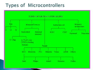
Explains microcontrollers as small computers on chips, comparing microcontrollers with microprocessors regarding features and usages.
Details about 8051, including RAM, ROM, I/O ports, timers, and its system architecture.
Discusses packaging types like DIP, QFP, FBGA and the necessity of efficient computing in embedded systems.
Features of the 8051 architecture, including ROM, RAM, timers, interrupts, and power supply requirements.
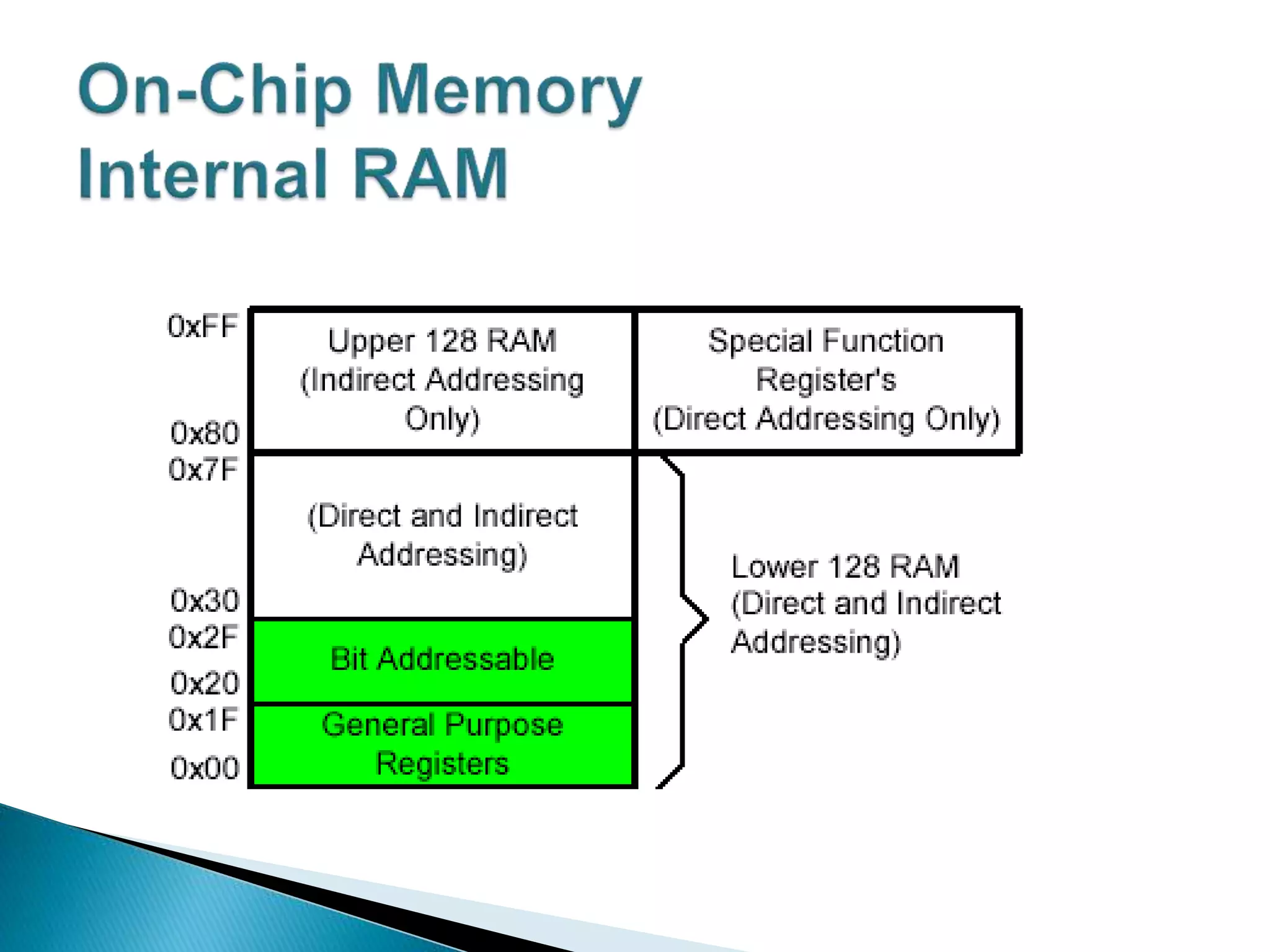
Details on the RAM and ROM layout, along with addressing and configuration of internal components.
Description of 8051 pin layout, functionalities of various ports, and pin-specific features like PSEN, ALE.
Comparison between Von Neumann and Harvard architectures, detailing control elements and memory components of the 8051.
RAM memory organization in the 8051, highlighting register banks and their addresses.
Explains various registers within the 8051, their utility, and hexadecimal notations.
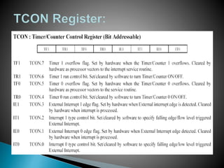
Describes handling of interrupts including priorities and enabling mechanisms in 8051.
Introduces RS-232 standard for serial communication, discussing wiring, voltage levels, and MAX232 converters.
Describes interfacing LCDs with the 8051, including initialization and commands for operation.
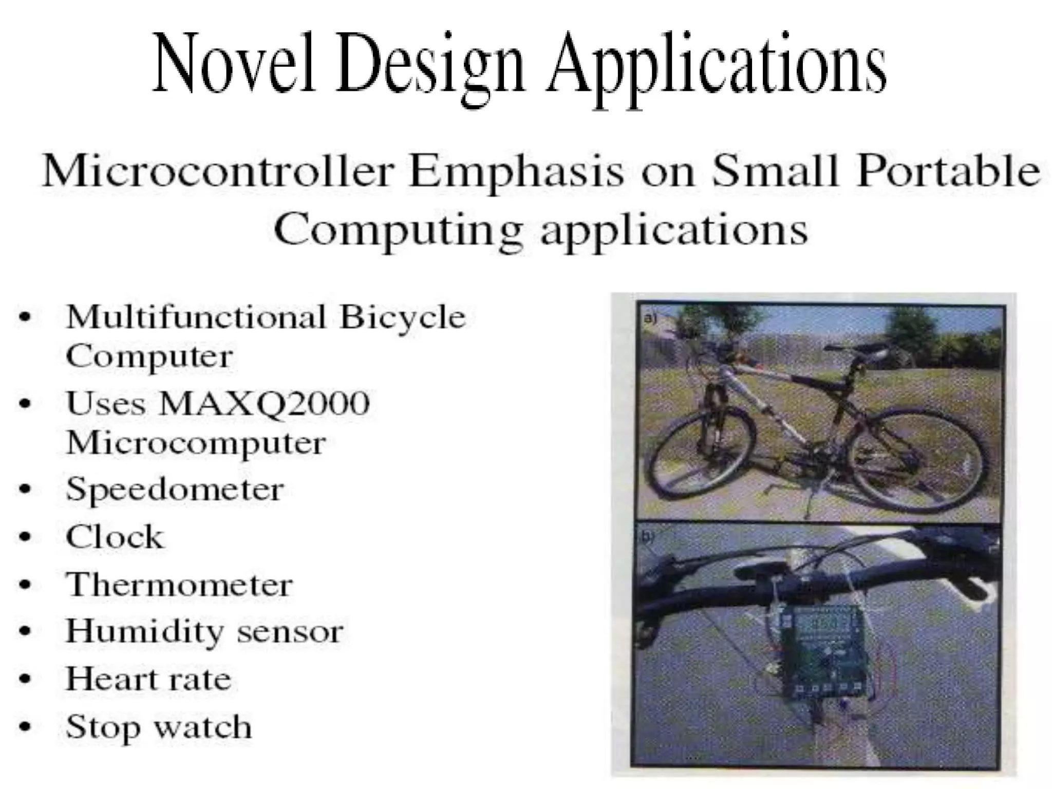
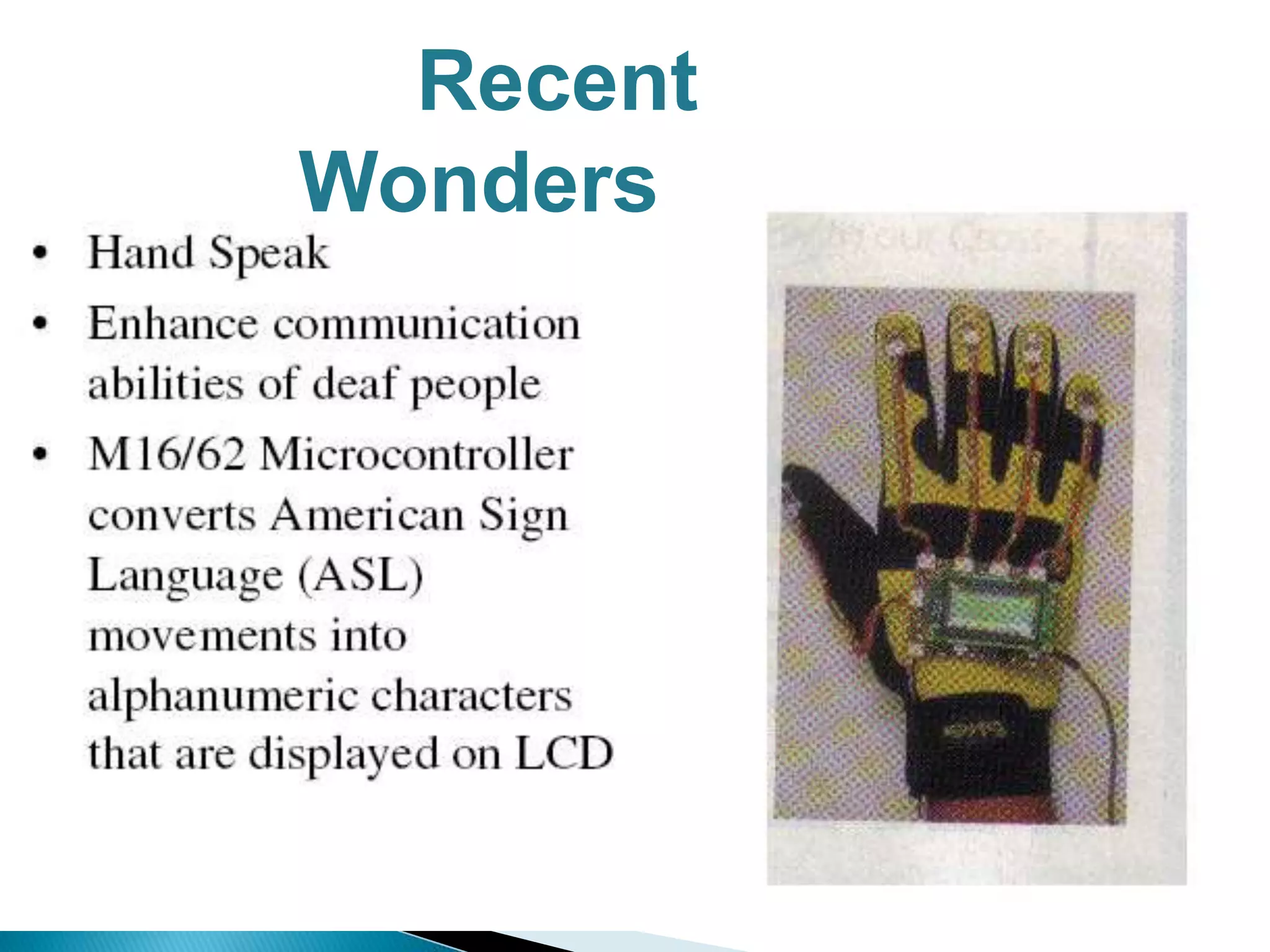
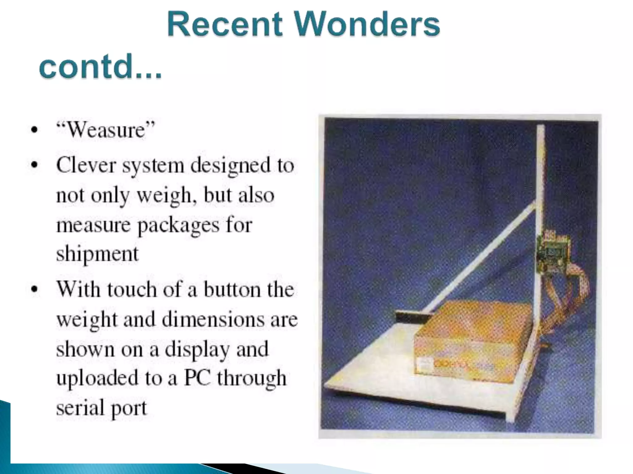
C language extensions aimed at embedded systems, highlighting memory areas and microcontroller applications.Various applications of microcontrollers in electronics today, emphasizing their widespread utility.
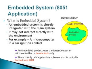
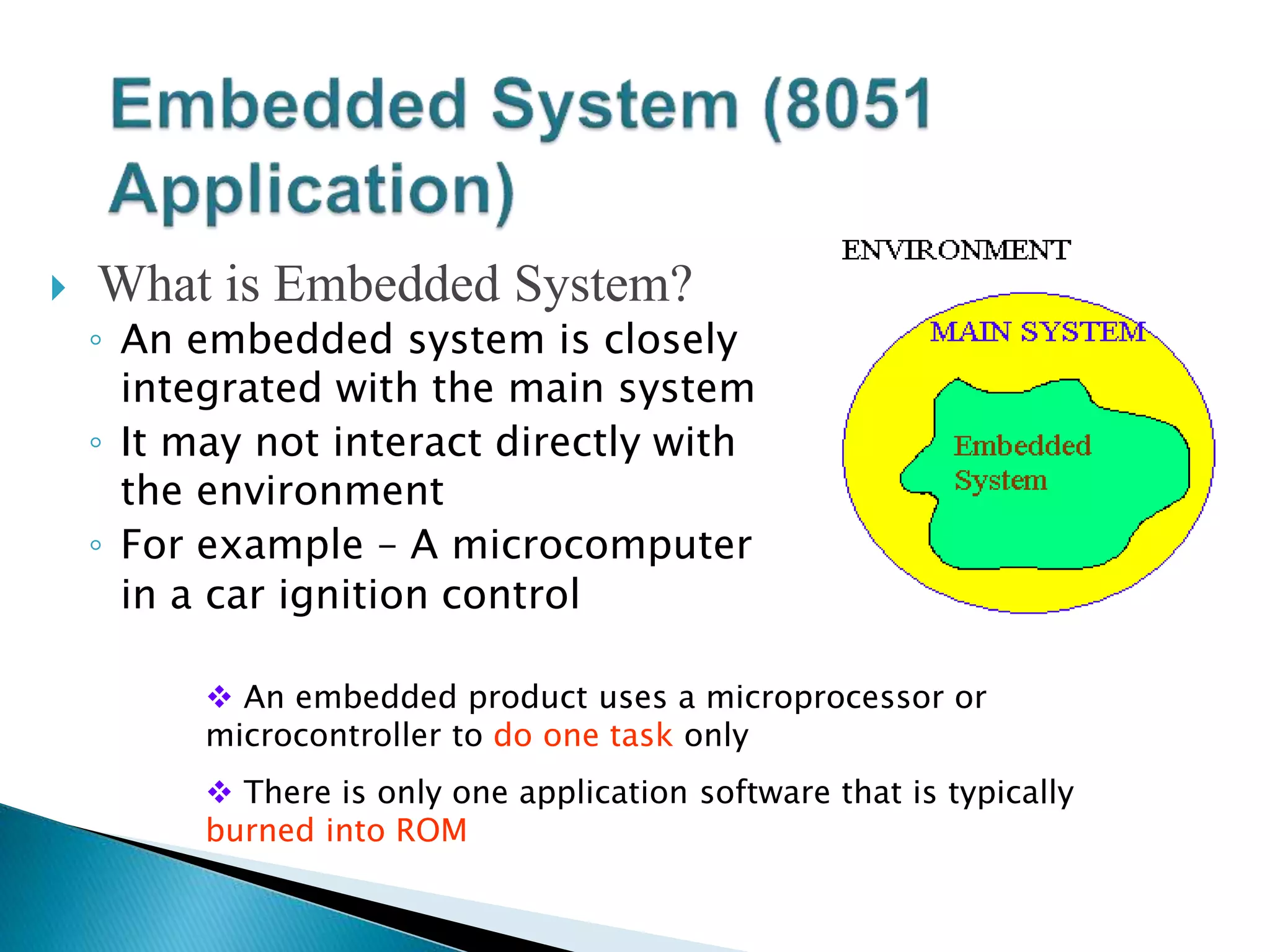
What isEmbedded System?
◦ An embedded system is closely
integrated with the main system
◦ It may not interact directly with
the environment
◦ For example – A microcomputer
in a car ignition control
An embedded product uses a microprocessor or
microcontroller to do one task only
There is only one application software that is typically
burned into ROM
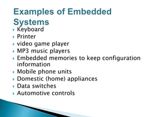
5.
Keyboard
Printer
video game player
MP3 music players
Embedded memories to keep configuration
information
Mobile phone units
Domestic (home) appliances
Data switches
Automotive controls
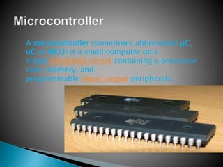
6.
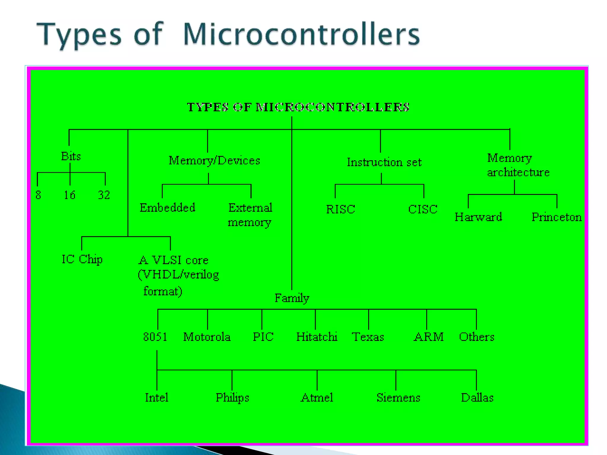
A microcontroller (sometimesabbreviated µC,
uC or MCU) is a small computer on a
single integrated circuit containing a processor
core, memory, and
programmable input/output peripherals.
7.
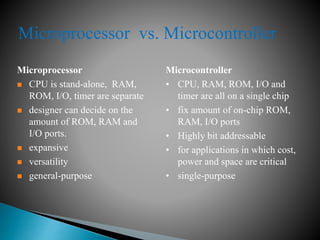
Microprocessor
CPU isstand-alone, RAM,
ROM, I/O, timer are separate
designer can decide on the
amount of ROM, RAM and
I/O ports.
expansive
versatility
general-purpose
Microcontroller
• CPU, RAM, ROM, I/O and
timer are all on a single chip
• fix amount of on-chip ROM,
RAM, I/O ports
• Highly bit addressable
• for applications in which cost,
power and space are critical
• single-purpose
Microprocessor vs. Microcontroller
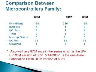
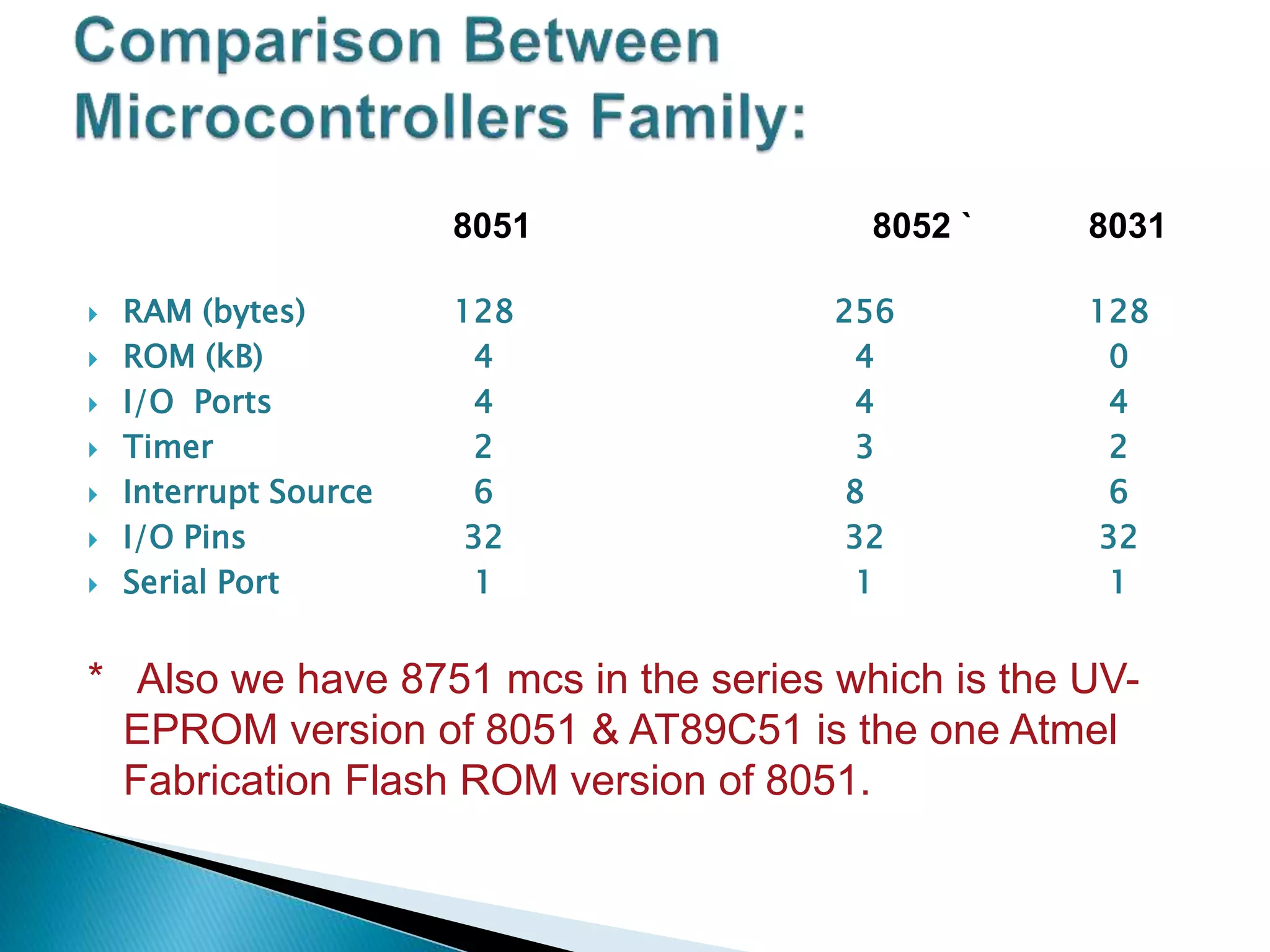
8.
8051 8052 `8031
RAM (bytes) 128 256 128
ROM (kB) 4 4 0
I/O Ports 4 4 4
Timer 2 3 2
Interrupt Source 6 8 6
I/O Pins 32 32 32
Serial Port 1 1 1
* Also we have 8751 mcs in the series which is the UV-
EPROM version of 8051 & AT89C51 is the one Atmel
Fabrication Flash ROM version of 8051.
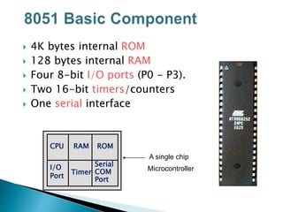
10.
4K bytesinternal ROM
128 bytes internal RAM
Four 8-bit I/O ports (P0 - P3).
Two 16-bit timers/counters
One serial interface
RAM
I/O
Port
Timer
Serial
COM
Port
Microcontroller
CPU
A single chip
ROM
11.
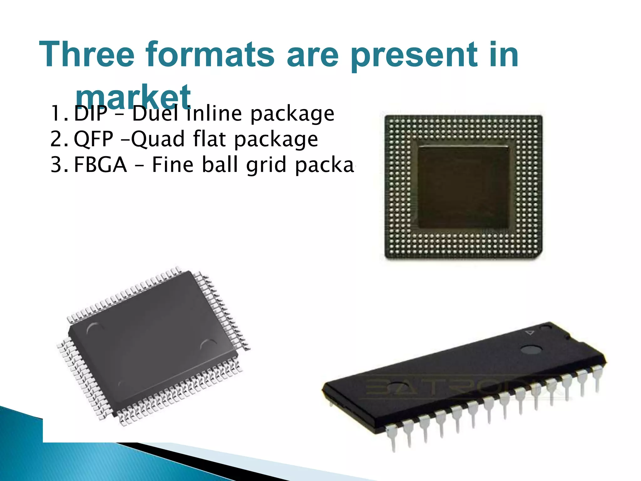
Three formats arepresent in
market1. DIP – Duel inline package
2. QFP –Quad flat package
3. FBGA – Fine ball grid package
FBGA
QFP
DIP
12.
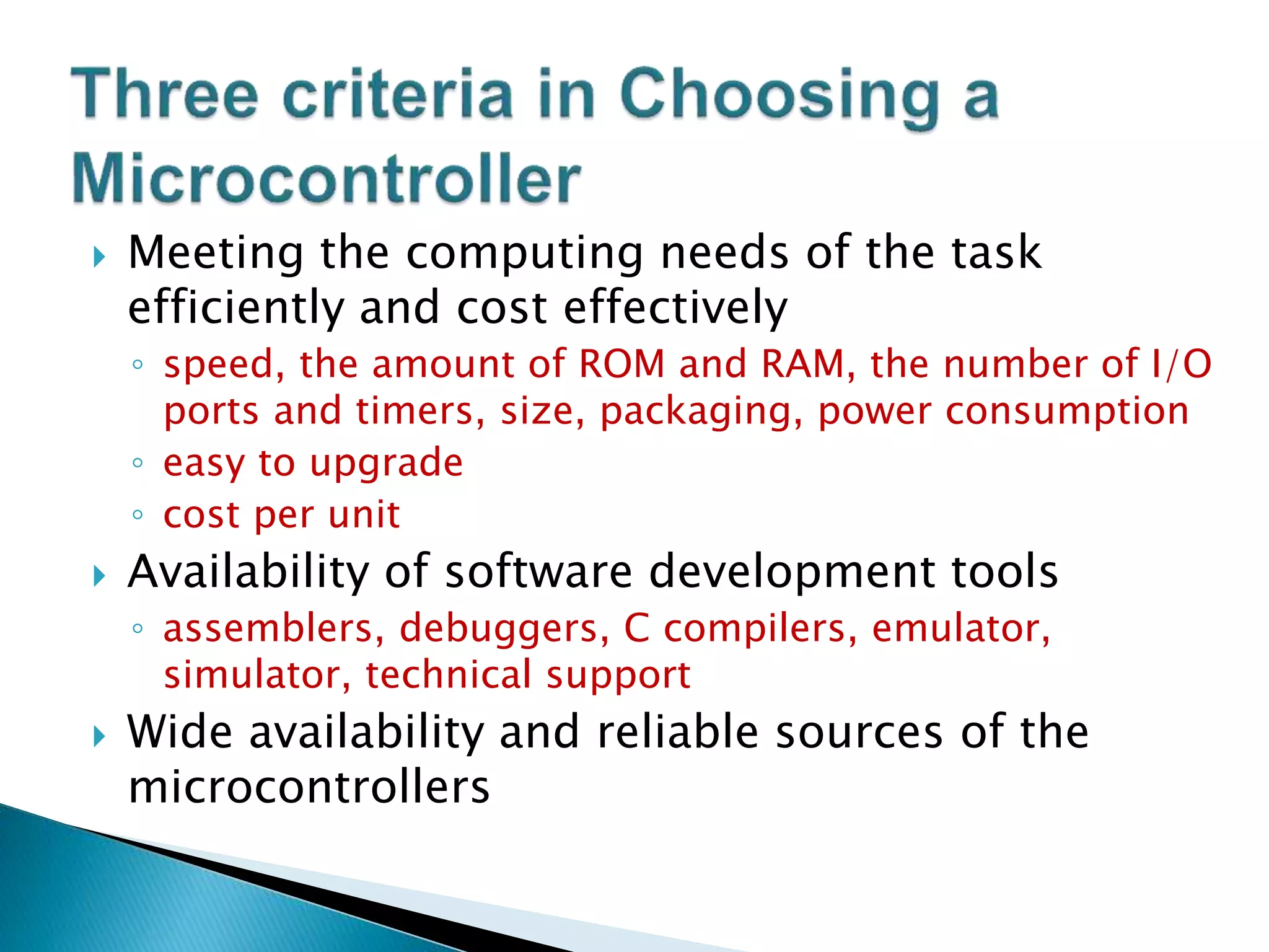
Meeting thecomputing needs of the task
efficiently and cost effectively
◦ speed, the amount of ROM and RAM, the number of I/O
ports and timers, size, packaging, power consumption
◦ easy to upgrade
◦ cost per unit
Availability of software development tools
◦ assemblers, debuggers, C compilers, emulator,
simulator, technical support
Wide availability and reliable sources of the
microcontrollers
13.
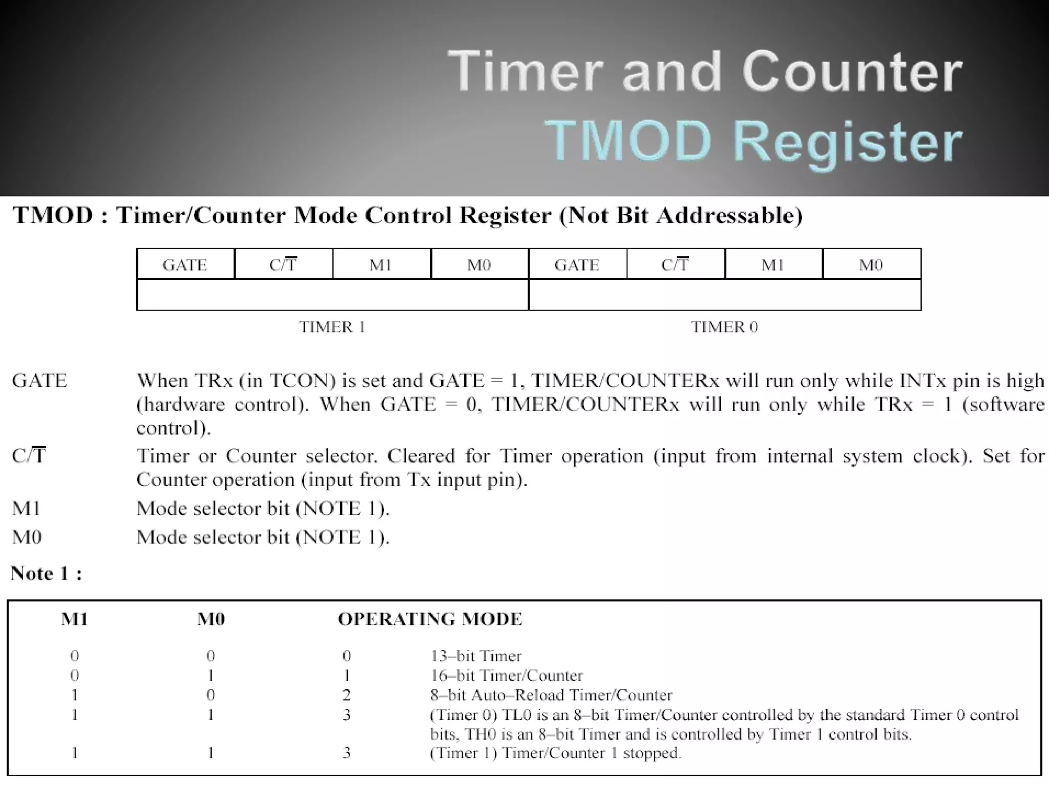
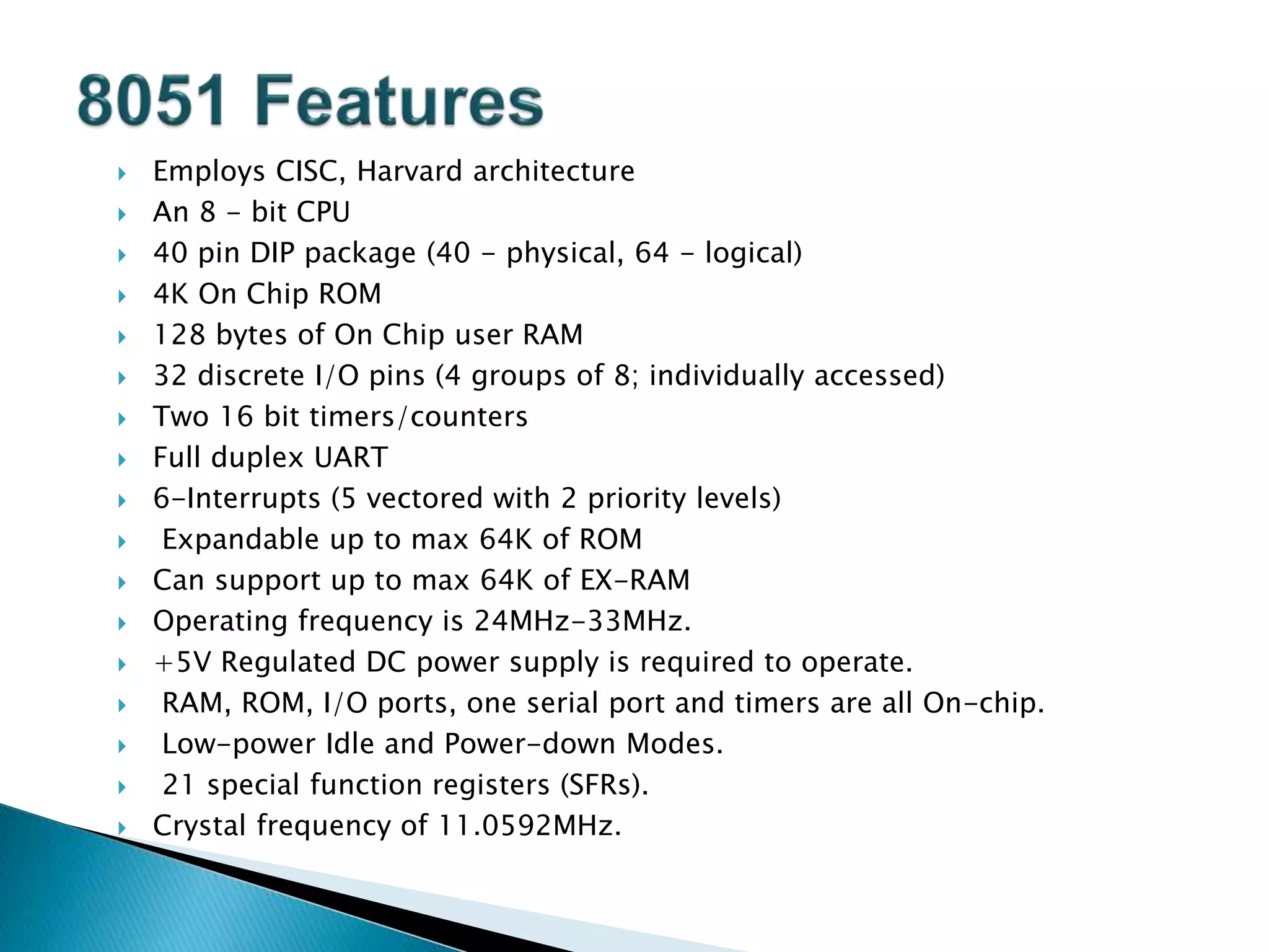
Employs CISC,Harvard architecture
An 8 - bit CPU
40 pin DIP package (40 - physical, 64 - logical)
4K On Chip ROM
128 bytes of On Chip user RAM
32 discrete I/O pins (4 groups of 8; individually accessed)
Two 16 bit timers/counters
Full duplex UART
6-Interrupts (5 vectored with 2 priority levels)
Expandable up to max 64K of ROM
Can support up to max 64K of EX-RAM
Operating frequency is 24MHz-33MHz.
+5V Regulated DC power supply is required to operate.
RAM, ROM, I/O ports, one serial port and timers are all On-chip.
Low-power Idle and Power-down Modes.
21 special function registers (SFRs).
Crystal frequency of 11.0592MHz.
14.
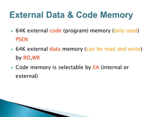
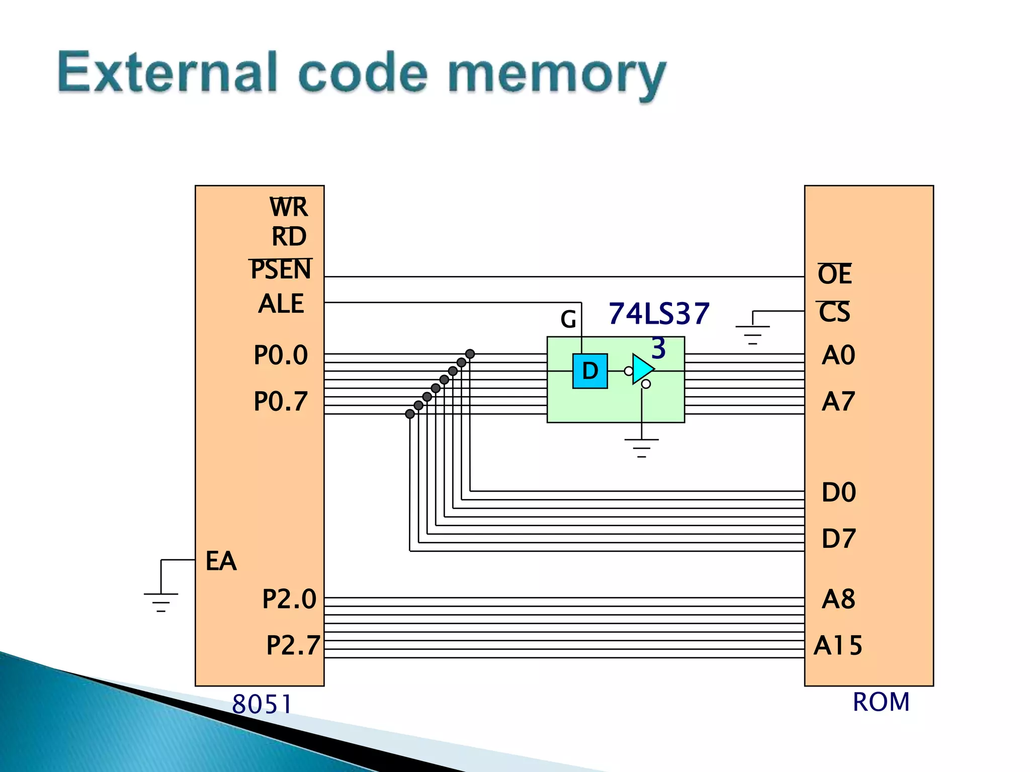
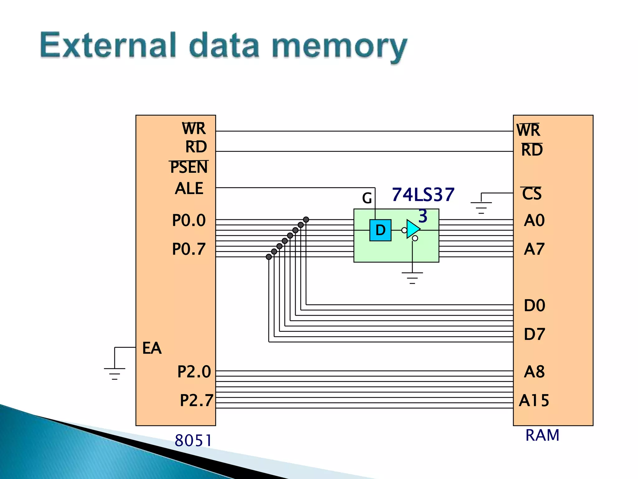
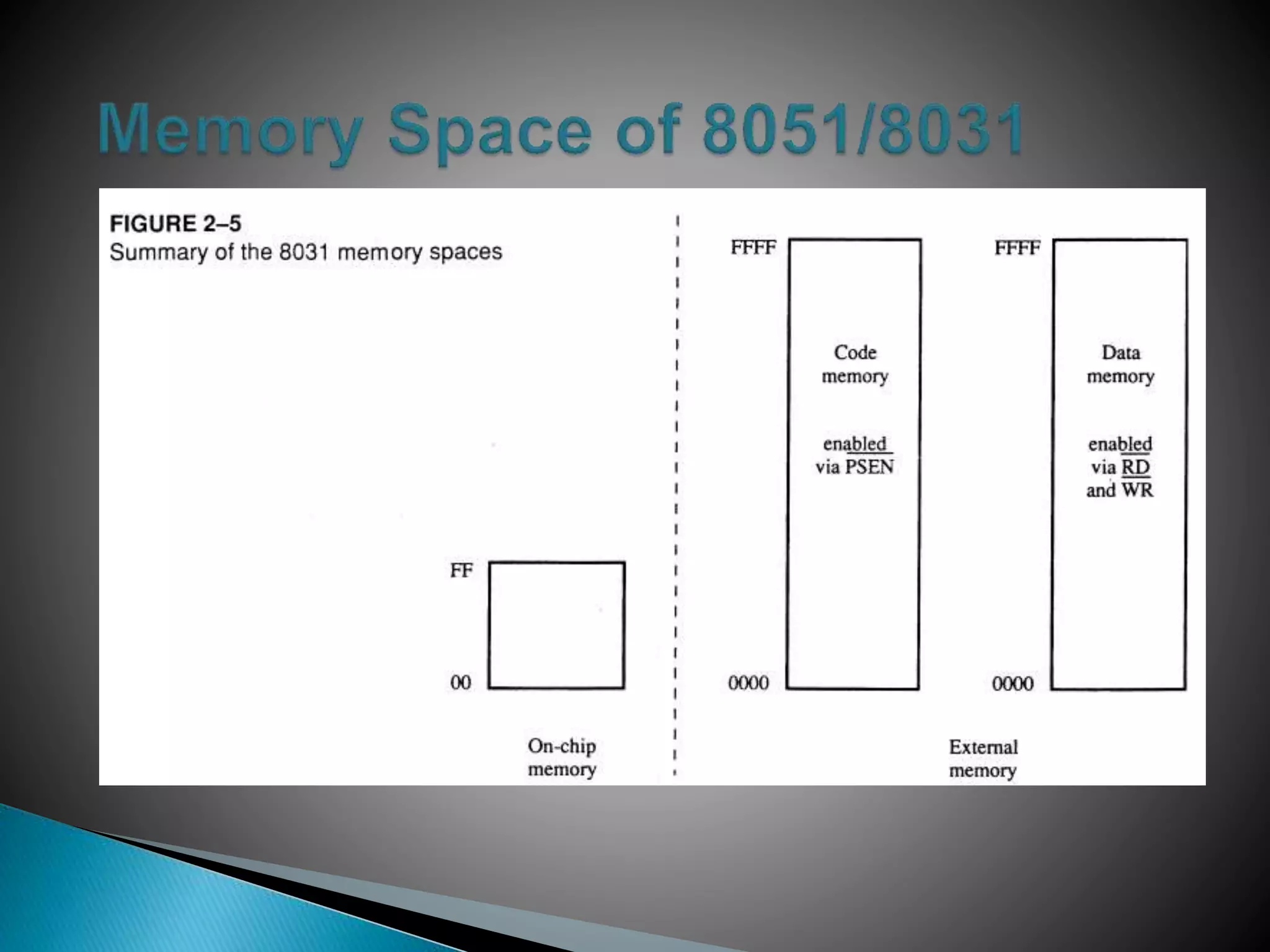
64K externalcode (program) memory (only read)
PSEN
64K external data memory (can be read and write)
by RD,WR
Code memory is selectable by EA (internal or
external)
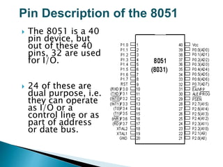
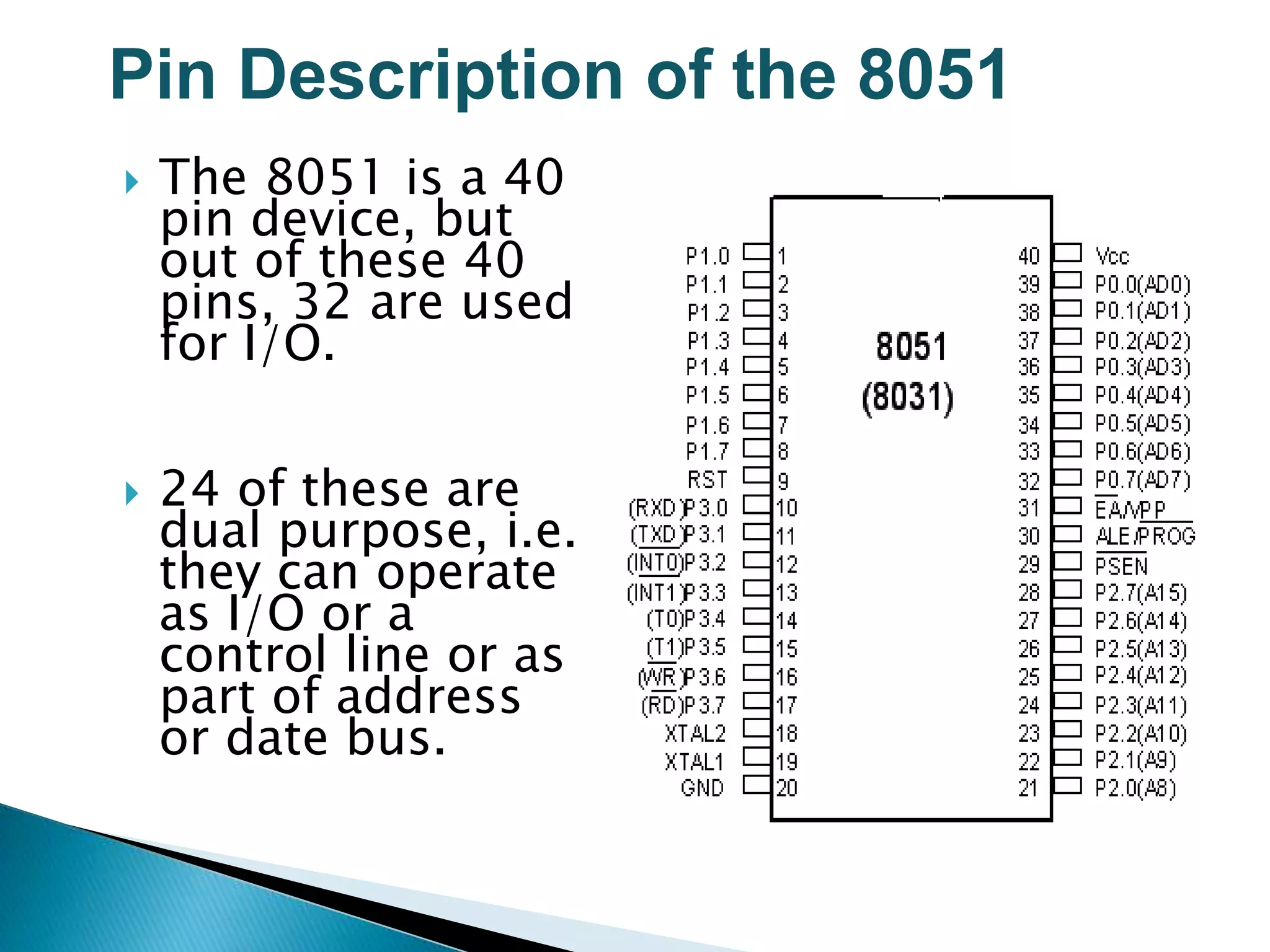
Pin Description ofthe 8051
The 8051 is a 40
pin device, but
out of these 40
pins, 32 are used
for I/O.
24 of these are
dual purpose, i.e.
they can operate
as I/O or a
control line or as
part of address
or date bus.
19.
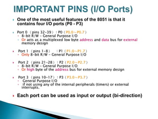
One ofthe most useful features of the 8051 is that it
contains four I/O ports (P0 - P3)
Port 0 (pins 32-39):P0(P0.0~P0.7)
◦ 8-bit R/W - General Purpose I/O
◦ Or acts as a multiplexed low byte address and data bus for external
memory design
Port 1 (pins 1-8) :P1(P1.0~P1.7)
◦ Only 8-bit R/W - General Purpose I/O
Port 2 (pins 21-28):P2(P2.0~P2.7)
◦ 8-bit R/W - General Purpose I/O
◦ Or high byte of the address bus for external memory design
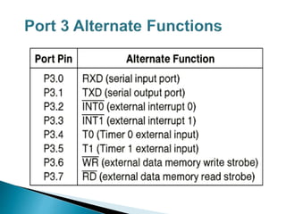
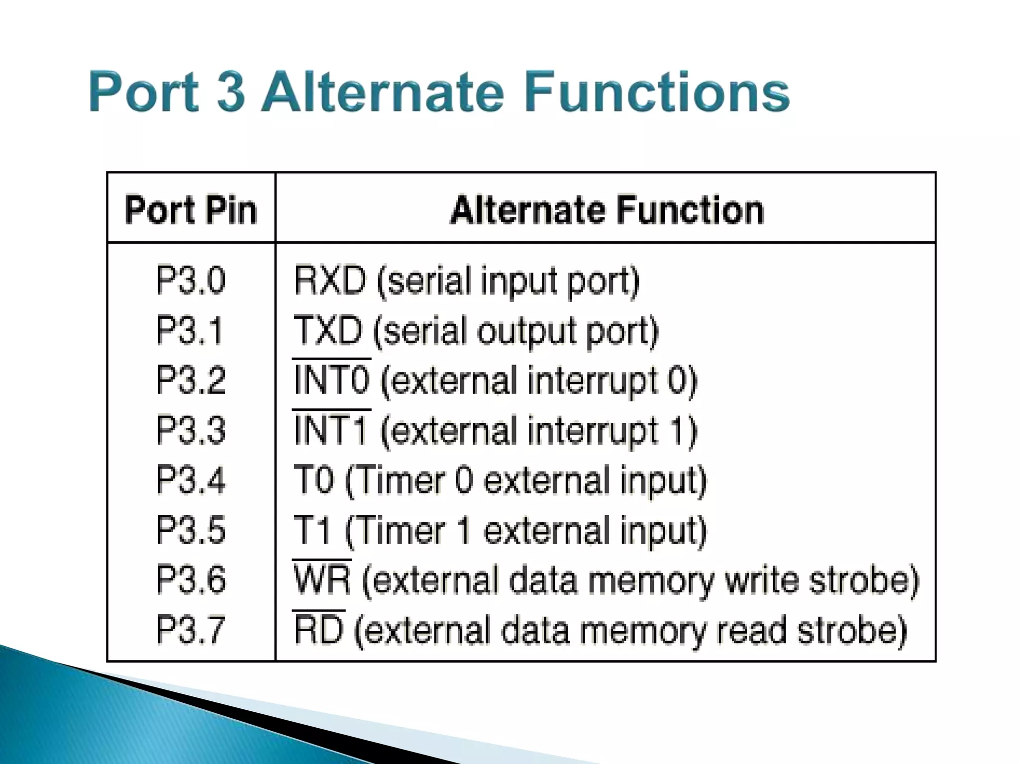
Port 3 (pins 10-17):P3(P3.0~P3.7)
◦ General Purpose I/O
◦ if not using any of the internal peripherals (timers) or external
interrupts.
Each port can be used as input or output (bi-direction)
20.
PSEN (out): ProgramStore Enable, the read
signal for external program memory (active
low).
ALE (out): Address Latch Enable, to latch
address outputs at Port0 and Port2
EA (in): External Access Enable, active low to
access external program memory locations 0 to
4K
RXD,TXD: UART pins for serial I/O on Port 3
◦ XTAL1 & XTAL2: Crystal inputs for internal
oscillator. These 2 pins provide external
clock.
◦ Way 1:using a quartz crystal oscillator
◦ Way 2:using a TTL oscillator
21.
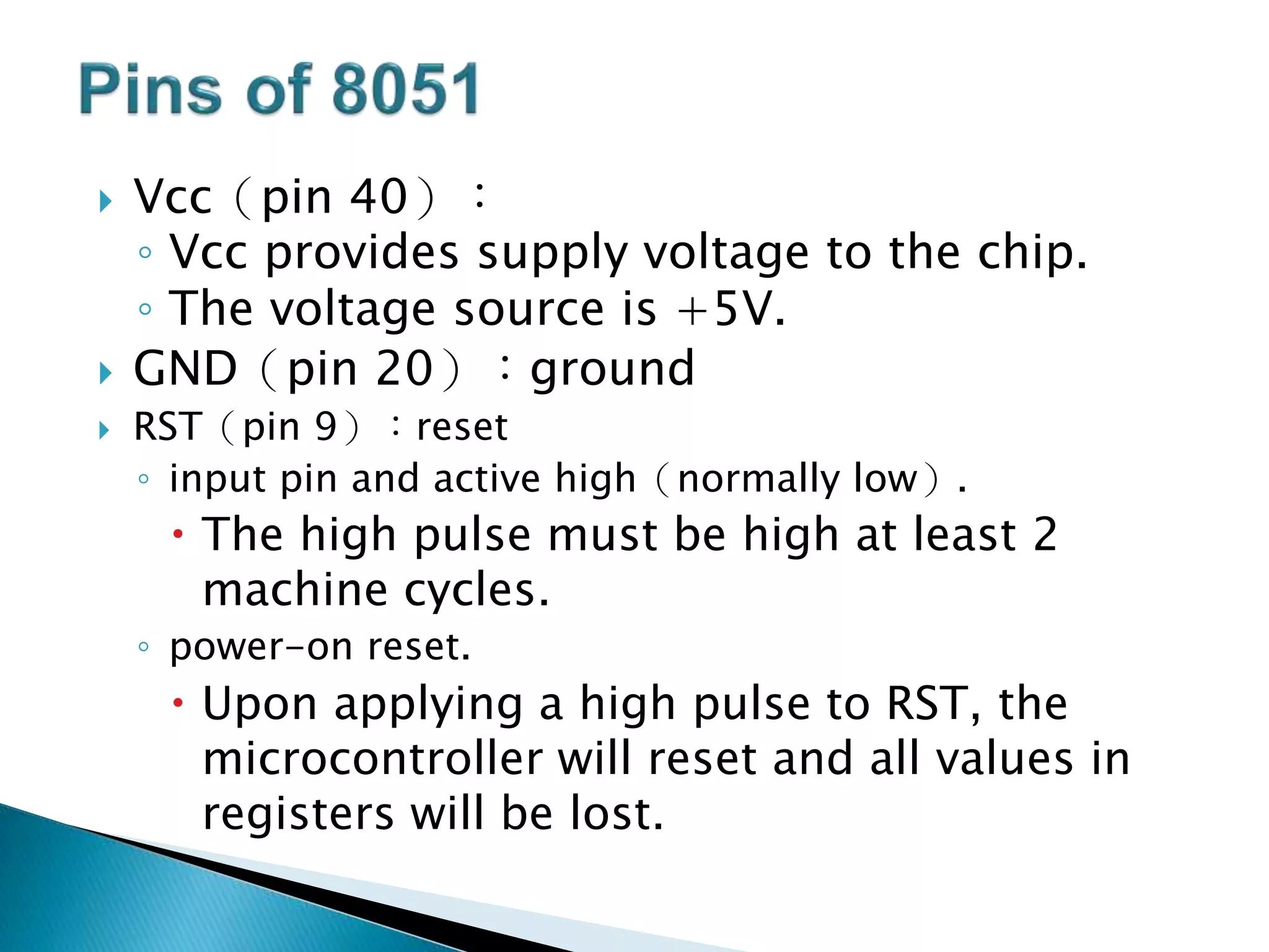
Vcc(pin 40):
◦Vcc provides supply voltage to the chip.
◦ The voltage source is +5V.
GND(pin 20):ground
RST(pin 9):reset
◦ input pin and active high(normally low).
The high pulse must be high at least 2
machine cycles.
◦ power-on reset.
Upon applying a high pulse to RST, the
microcontroller will reset and all values in
registers will be lost.
22.
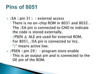
/EA(pin 31):externalaccess
◦ There is no on-chip ROM in 8031 and 8032 .
◦ The /EA pin is connected to GND to indicate
the code is stored externally.
◦ /PSEN & ALE are used for external ROM.
◦ For 8051, /EA pin is connected to Vcc.
◦ “/” means active low.
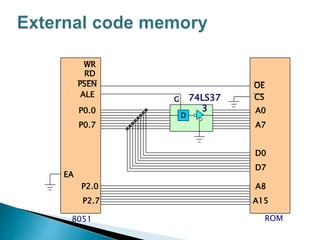
/PSEN(pin 29):program store enable
◦ This is an output pin and is connected to the
OE pin of the ROM.
23.
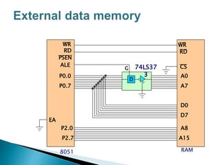
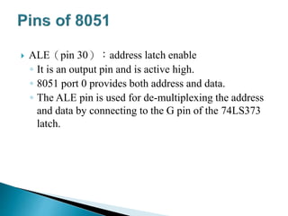
ALE(pin 30):addresslatch enable
◦ It is an output pin and is active high.
◦ 8051 port 0 provides both address and data.
◦ The ALE pin is used for de-multiplexing the address
and data by connecting to the G pin of the 74LS373
latch.
25.
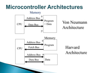
CPU
Program
+ Data
Address Bus
DataBus
Memory
Von Neumann
Architecture
CPU
Program
Address Bus
Data Bus
Harvard
Architecture
Memory
Data
Address Bus
Fetch Bus
0
0
0
2n
26.
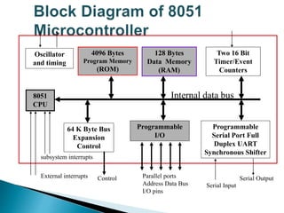
Oscillator
and timing
4096 Bytes
ProgramMemory
(ROM)
128 Bytes
Data Memory
(RAM)
Two 16 Bit
Timer/Event
Counters
8051
CPU
64 K Byte Bus
Expansion
Control
Programmable
I/O
Programmable
Serial Port Full
Duplex UART
Synchronous Shifter
Internal data bus
External interrupts
subsystem interrupts
Control Parallel ports
Address Data Bus
I/O pins
Serial Input
Serial Output
29.
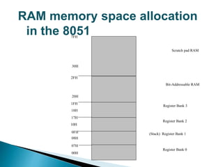
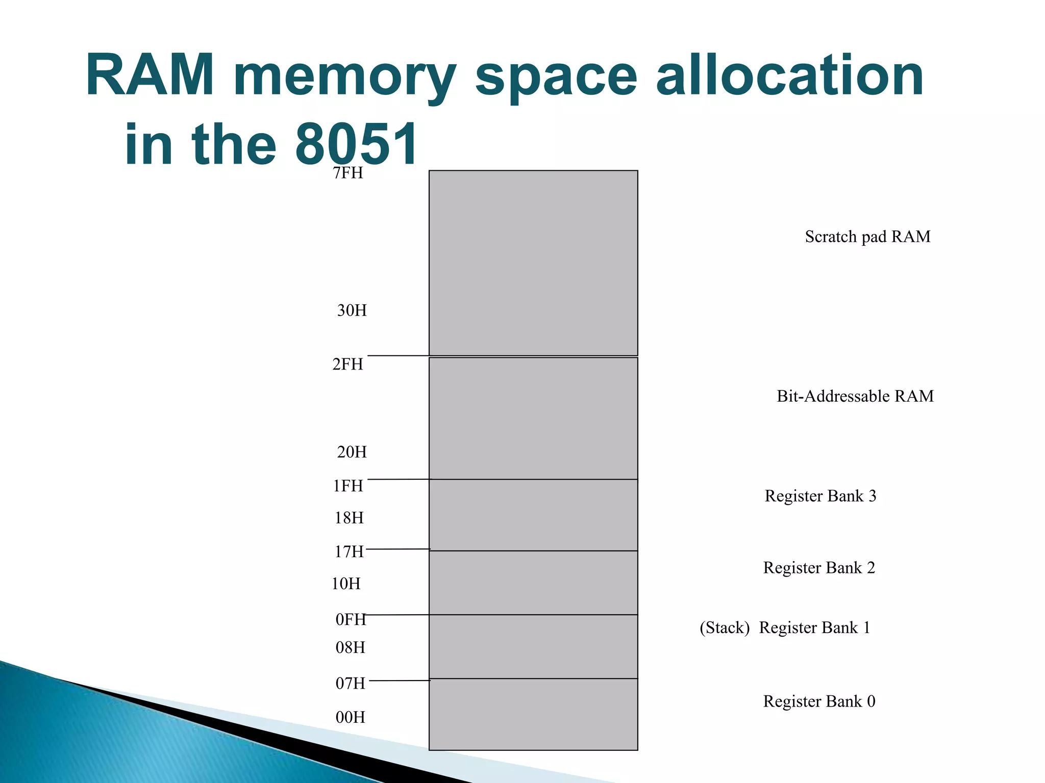
RAM memory spaceallocation
in the 80517FH
30H
2FH
20H
1FH
17H
10H
0FH
07H
08H
18H
00H
Register Bank 0
(Stack) Register Bank 1
Register Bank 2
Register Bank 3
Bit-Addressable RAM
Scratch pad RAM
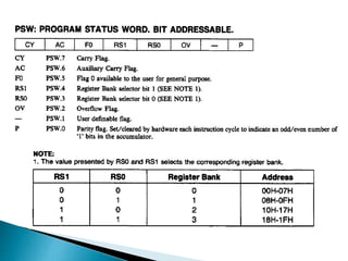
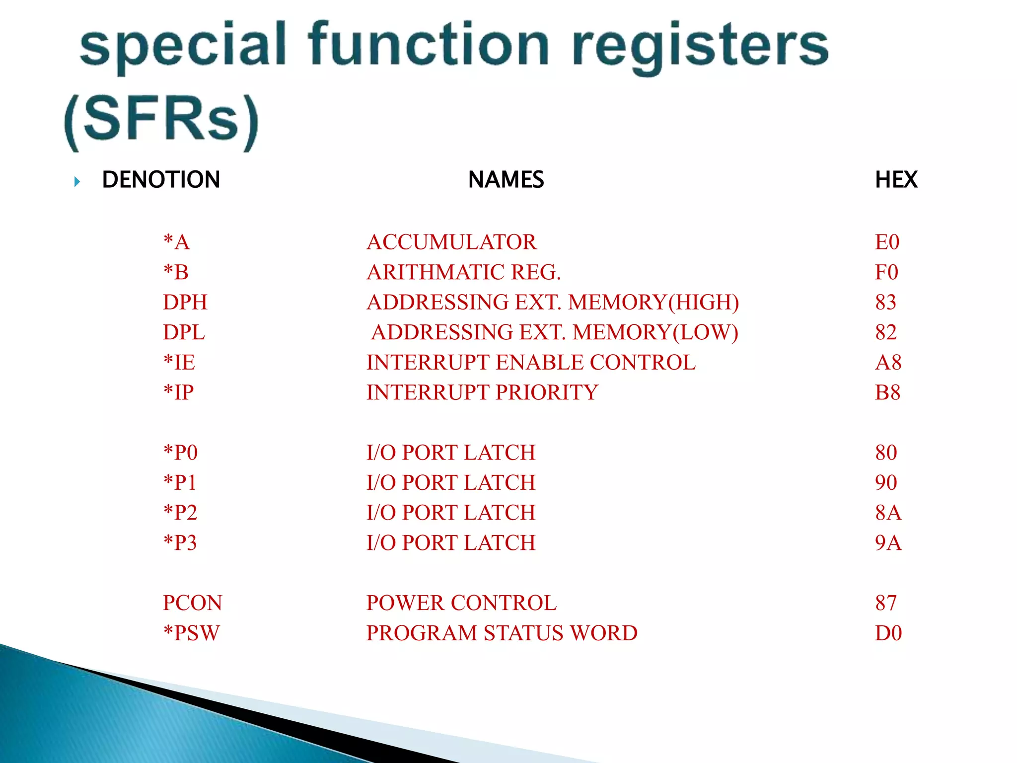
DENOTION NAMESHEX
*A ACCUMULATOR E0
*B ARITHMATIC REG. F0
DPH ADDRESSING EXT. MEMORY(HIGH) 83
DPL ADDRESSING EXT. MEMORY(LOW) 82
*IE INTERRUPT ENABLE CONTROL A8
*IP INTERRUPT PRIORITY B8
*P0 I/O PORT LATCH 80
*P1 I/O PORT LATCH 90
*P2 I/O PORT LATCH 8A
*P3 I/O PORT LATCH 9A
PCON POWER CONTROL 87
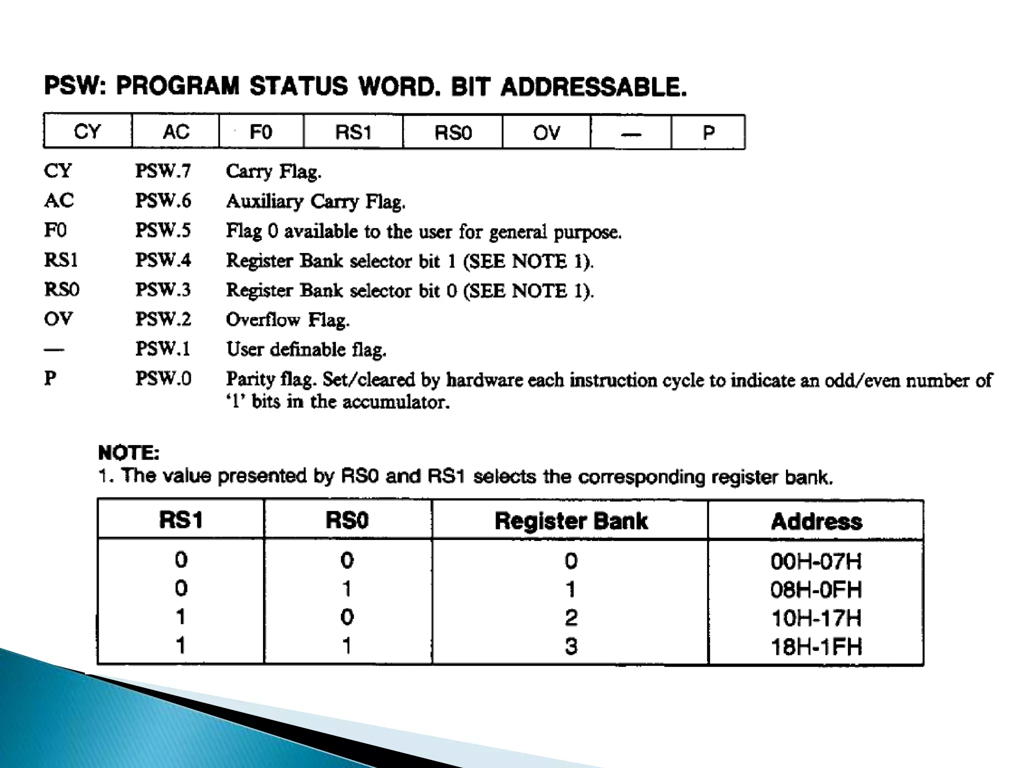
*PSW PROGRAM STATUS WORD D0
32.
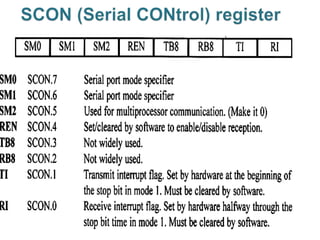
*SCON SERIAL PORTCONTROL 98
SBUF SERIAL DATA BUFFER 99
SP STACK POINTER 81
TMOD TIMER/COUNTER MODE CONTROL 8B
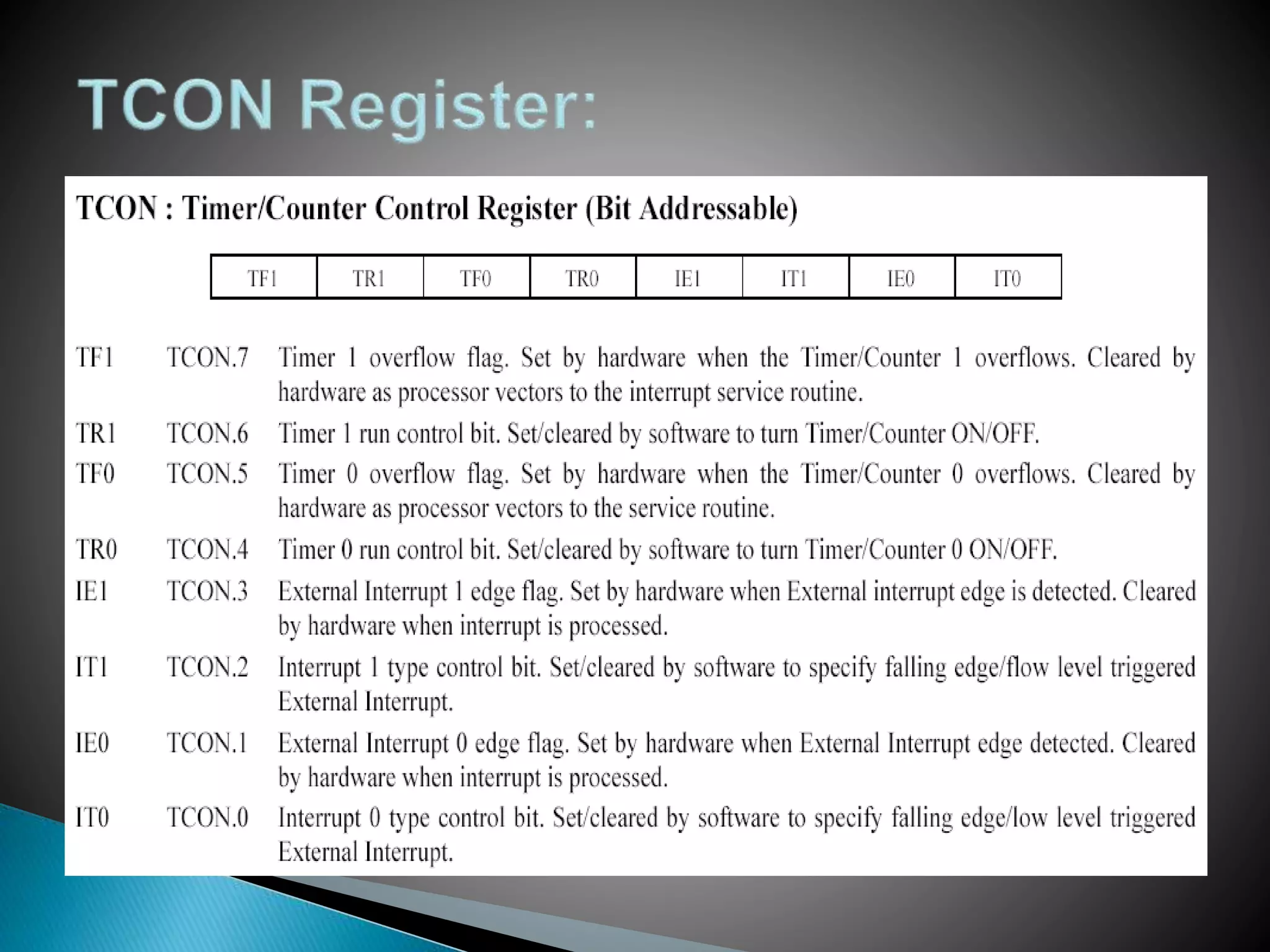
*TCON TIMER/COUNTER CONTROL 89
TH0 TIMER O HIGH BYTE 8C
TLO TIMER 0 LOWER BYTE 8A
TH1 TIMER 1 HIGH BYTE 8D
TL1 TIMER 1 LOWER BYTE 8B
33.
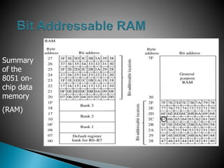
Four banksof 8 byte-sized registers, R0 to R7
Addresses are :
18 - 1F for bank 3
10 - 17 for bank 2
08 - 0F for bank 1
00 - 07 for bank 0 (default)
Active bank selected by bits [ RS1, RS0 ] in
PSW.
Permits fast “context switching” in interrupt
service routines (ISR).
38.
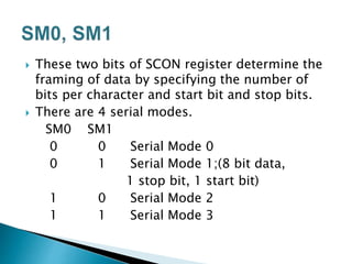
These twobits of SCON register determine the
framing of data by specifying the number of
bits per character and start bit and stop bits.
There are 4 serial modes.
SM0 SM1
0 0 Serial Mode 0
0 1 Serial Mode 1;(8 bit data,
1 stop bit, 1 start bit)
1 0 Serial Mode 2
1 1 Serial Mode 3
39.
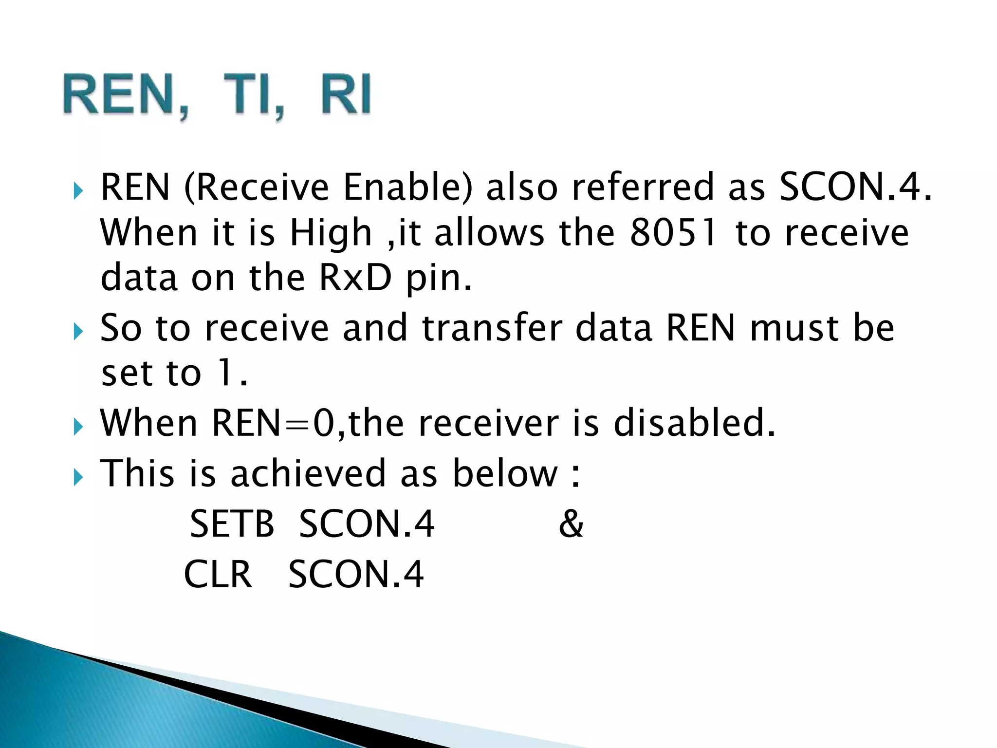
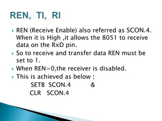
REN (ReceiveEnable) also referred as SCON.4.
When it is High ,it allows the 8051 to receive
data on the RxD pin.
So to receive and transfer data REN must be
set to 1.
When REN=0,the receiver is disabled.
This is achieved as below :
SETB SCON.4 &
CLR SCON.4
40.
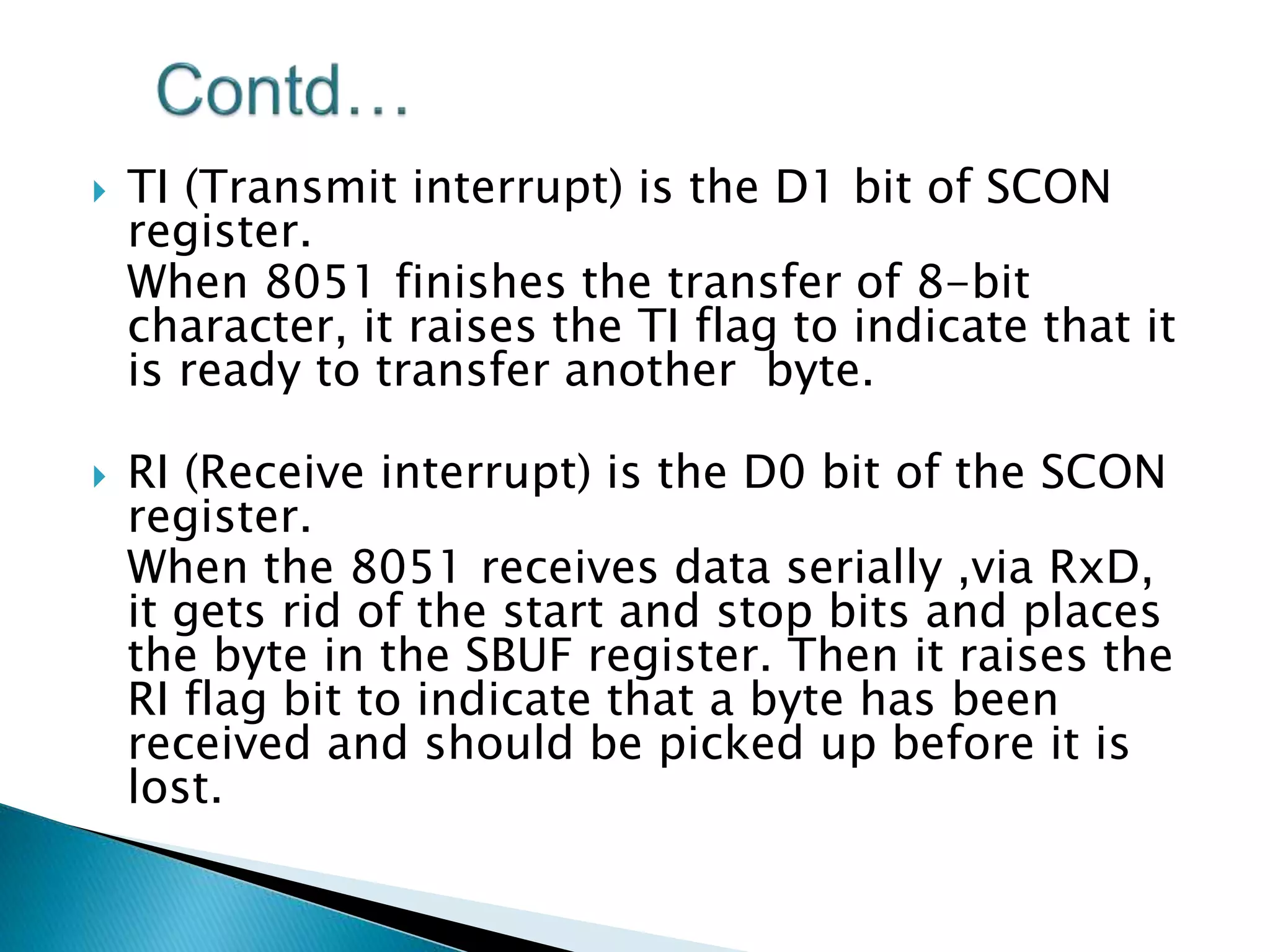
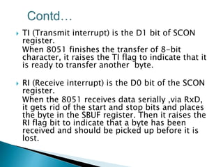
TI (Transmitinterrupt) is the D1 bit of SCON
register.
When 8051 finishes the transfer of 8-bit
character, it raises the TI flag to indicate that it
is ready to transfer another byte.
RI (Receive interrupt) is the D0 bit of the SCON
register.
When the 8051 receives data serially ,via RxD,
it gets rid of the start and stop bits and places
the byte in the SBUF register. Then it raises the
RI flag bit to indicate that a byte has been
received and should be picked up before it is
lost.
41.
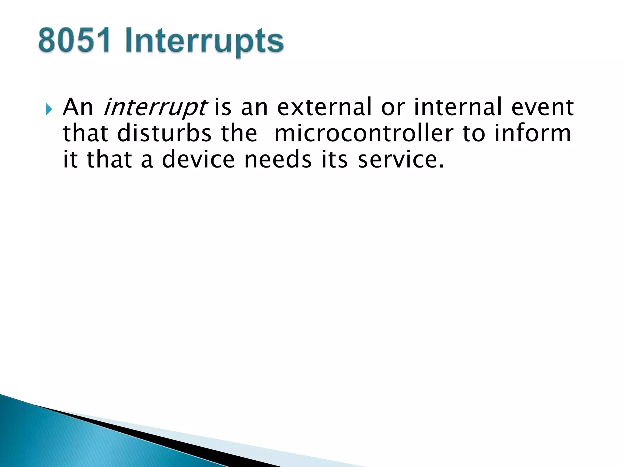
An interruptis an external or internal event
that disturbs the microcontroller to inform
it that a device needs its service.
42.
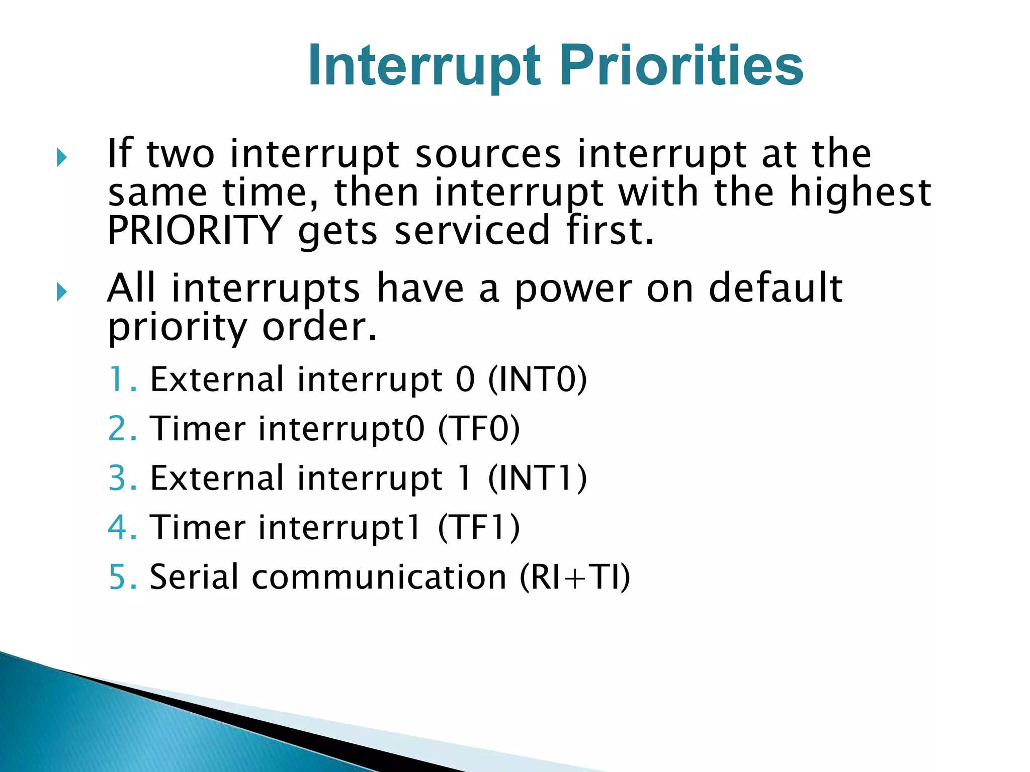
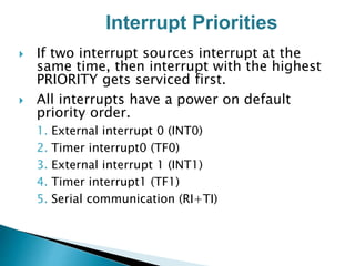
If twointerrupt sources interrupt at the
same time, then interrupt with the highest
PRIORITY gets serviced first.
All interrupts have a power on default
priority order.
1. External interrupt 0 (INT0)
2. Timer interrupt0 (TF0)
3. External interrupt 1 (INT1)
4. Timer interrupt1 (TF1)
5. Serial communication (RI+TI)
Interrupt Priorities
43.
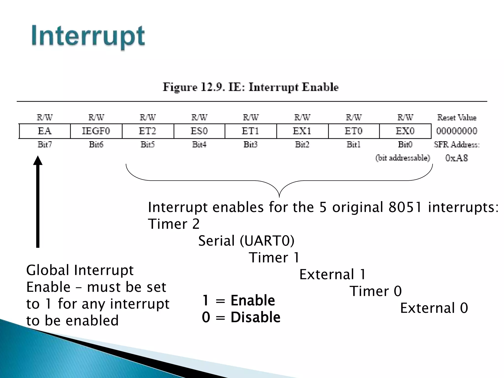
Global Interrupt
Enable –must be set
to 1 for any interrupt
to be enabled
Interrupt enables for the 5 original 8051 interrupts:
Timer 2
Serial (UART0)
Timer 1
External 1
Timer 0
External 0
1 = Enable
0 = Disable
44.
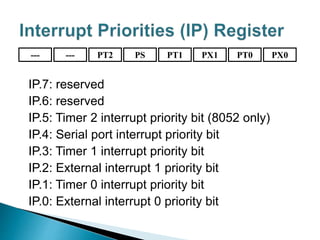
IP.7: reserved
IP.6: reserved
IP.5:Timer 2 interrupt priority bit (8052 only)
IP.4: Serial port interrupt priority bit
IP.3: Timer 1 interrupt priority bit
IP.2: External interrupt 1 priority bit
IP.1: Timer 0 interrupt priority bit
IP.0: External interrupt 0 priority bit
--- PX0PT0PX1PT1PSPT2---
45.
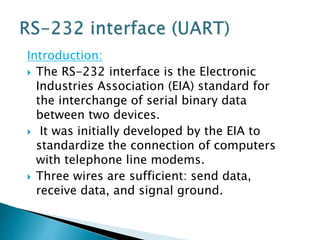
Introduction:
The RS-232interface is the Electronic
Industries Association (EIA) standard for
the interchange of serial binary data
between two devices.
It was initially developed by the EIA to
standardize the connection of computers
with telephone line modems.
Three wires are sufficient: send data,
receive data, and signal ground.
46.
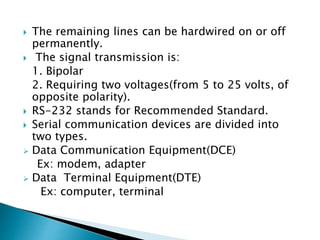
The remaininglines can be hardwired on or off
permanently.
The signal transmission is:
1. Bipolar
2. Requiring two voltages(from 5 to 25 volts, of
opposite polarity).
RS-232 stands for Recommended Standard.
Serial communication devices are divided into
two types.
Data Communication Equipment(DCE)
Ex: modem, adapter
Data Terminal Equipment(DTE)
Ex: computer, terminal
47.
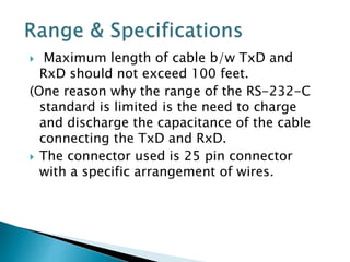
Maximum lengthof cable b/w TxD and
RxD should not exceed 100 feet.
(One reason why the range of the RS-232-C
standard is limited is the need to charge
and discharge the capacitance of the cable
connecting the TxD and RxD.
The connector used is 25 pin connector
with a specific arrangement of wires.
48.
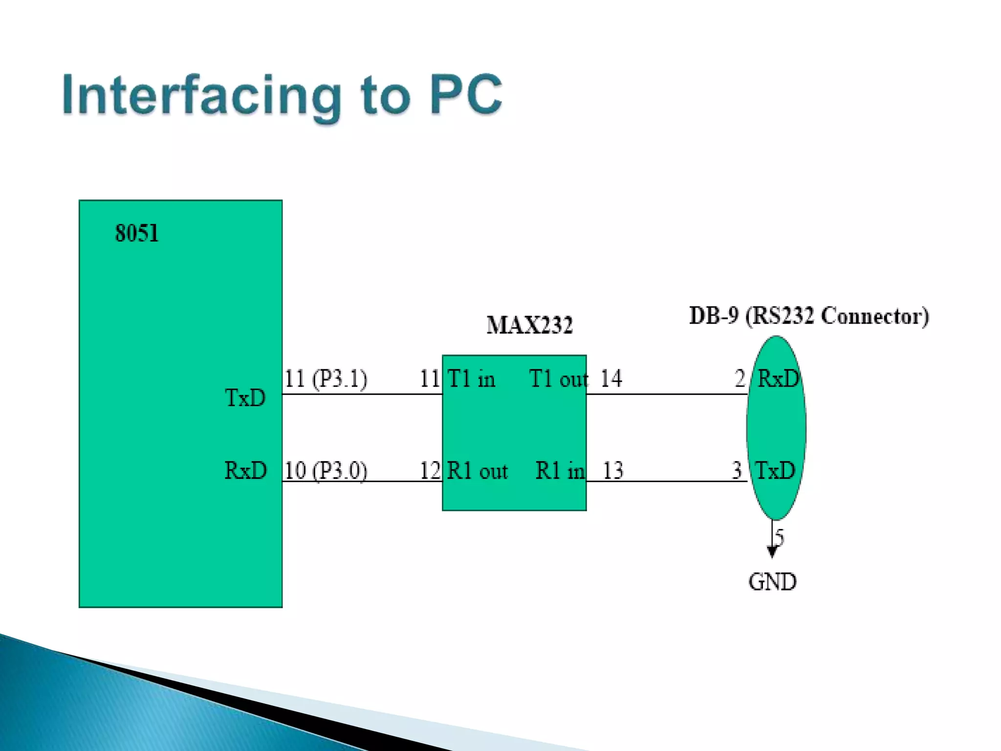
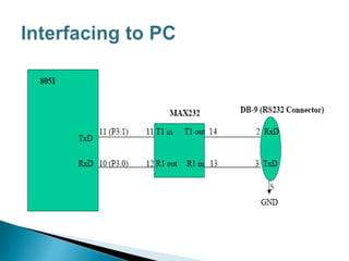
MAX232 (Level Convertor)
*Usually, all Digital ICs
work on TTL or CMOS
voltage Level which
can’t be used to
communicate over
RS232 protocol. So, a
voltage convertor is
needed to convert
such levels.
* The most commonly
used RS-232 level
convertor is MAX232.
* It consist two Tx &
Rx and is capable of
Full Duplex UART
50.
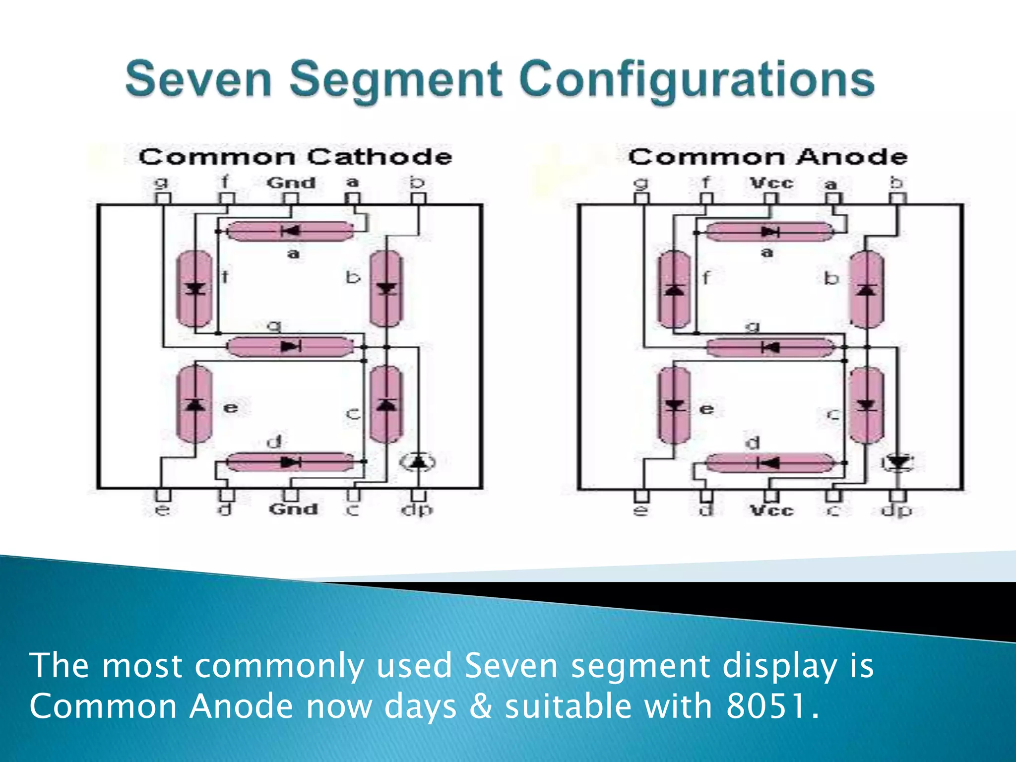
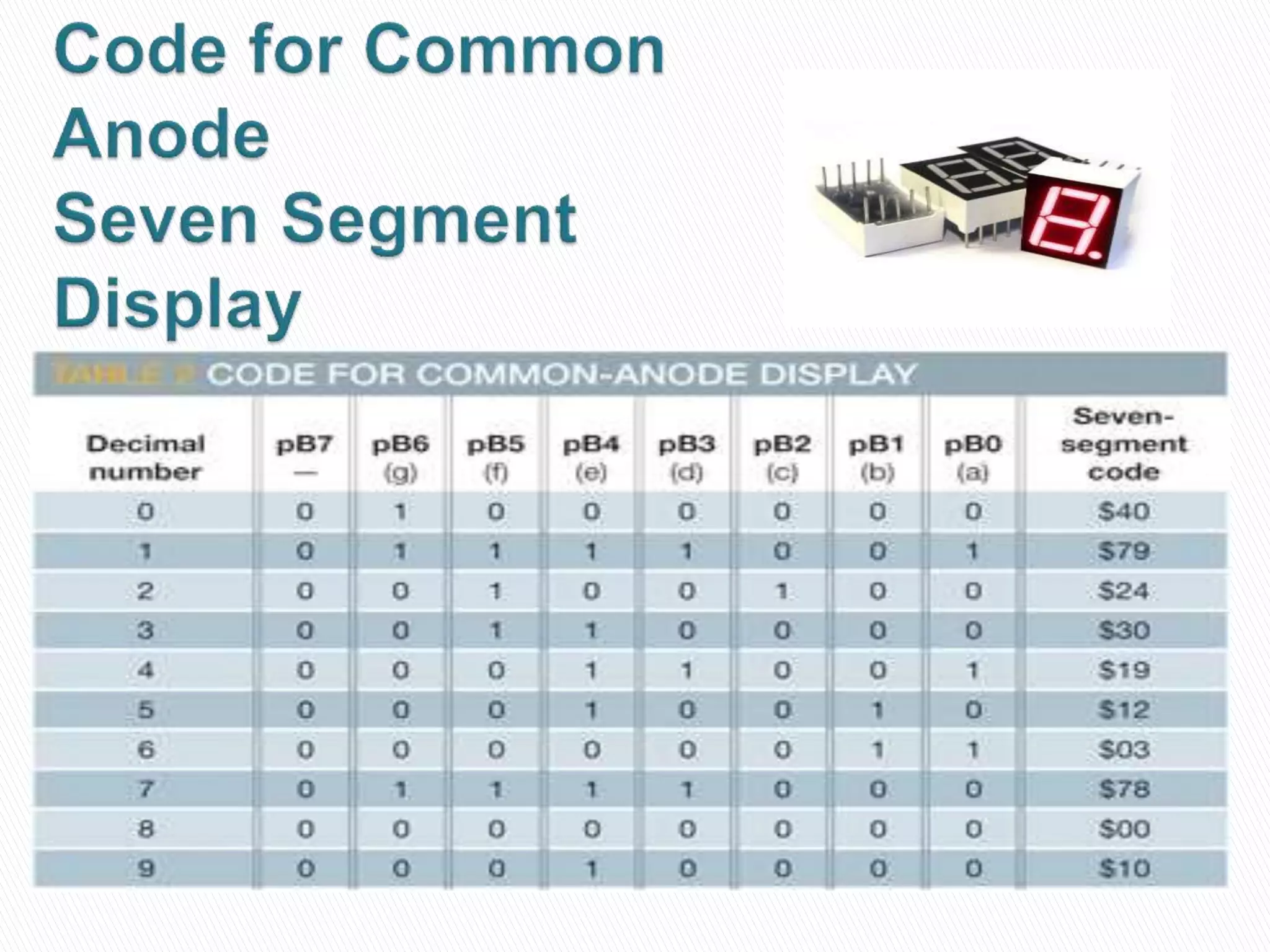
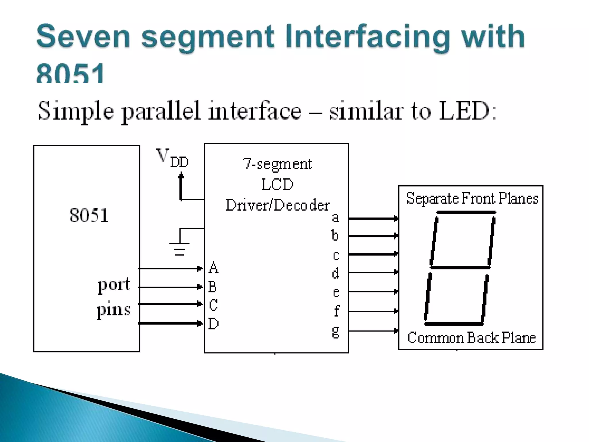
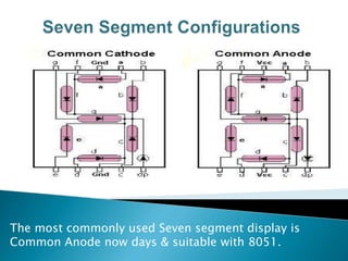
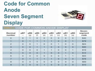
The most commonlyused Seven segment display is
Common Anode now days & suitable with 8051.
53.
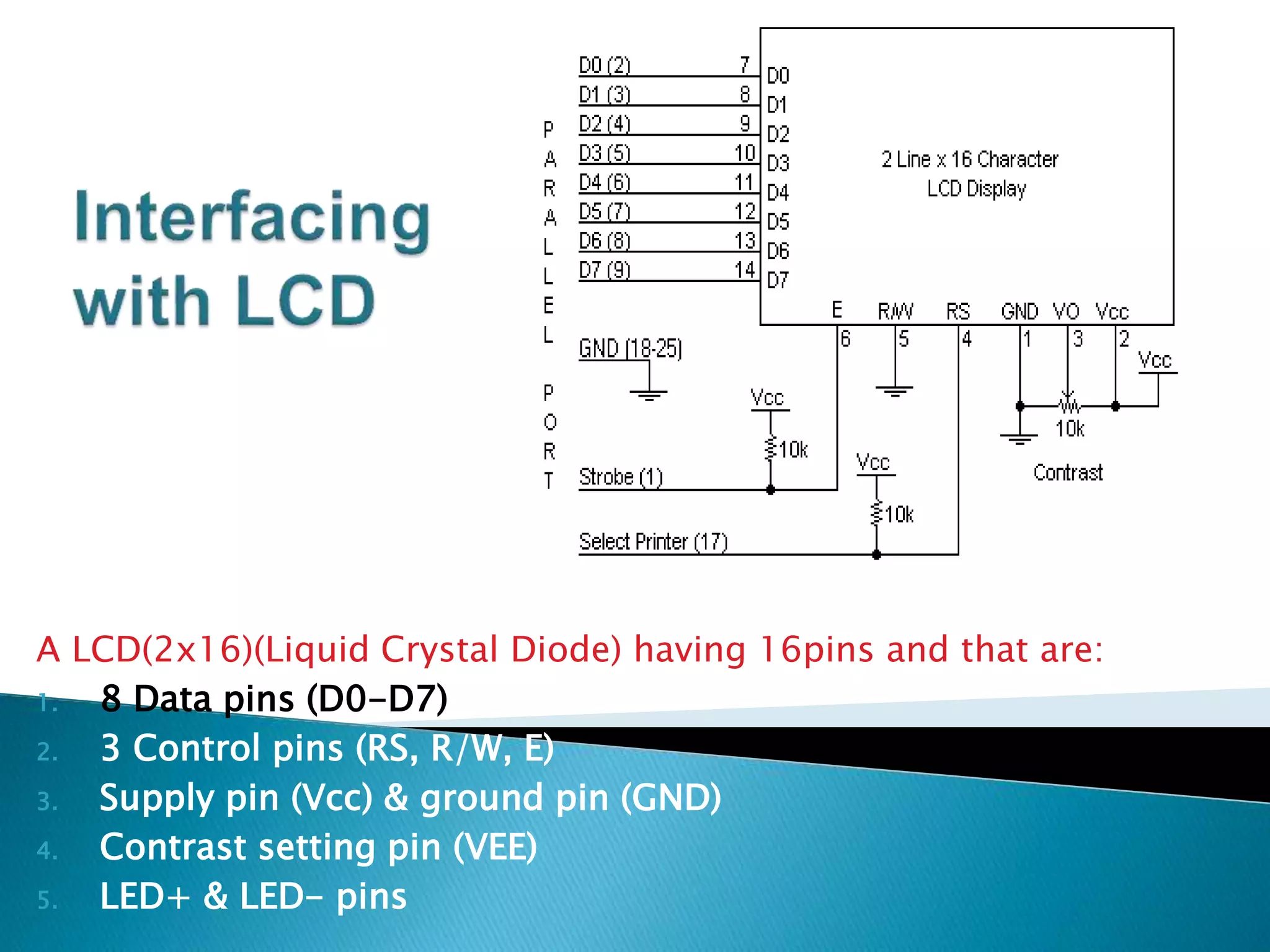
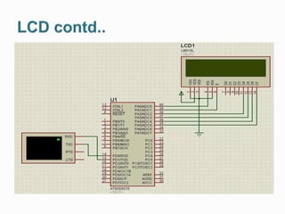
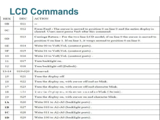
A LCD(2x16)(Liquid CrystalDiode) having 16pins and that are:
1. 8 Data pins (D0-D7)
2. 3 Control pins (RS, R/W, E)
3. Supply pin (Vcc) & ground pin (GND)
4. Contrast setting pin (VEE)
5. LED+ & LED- pins
55.
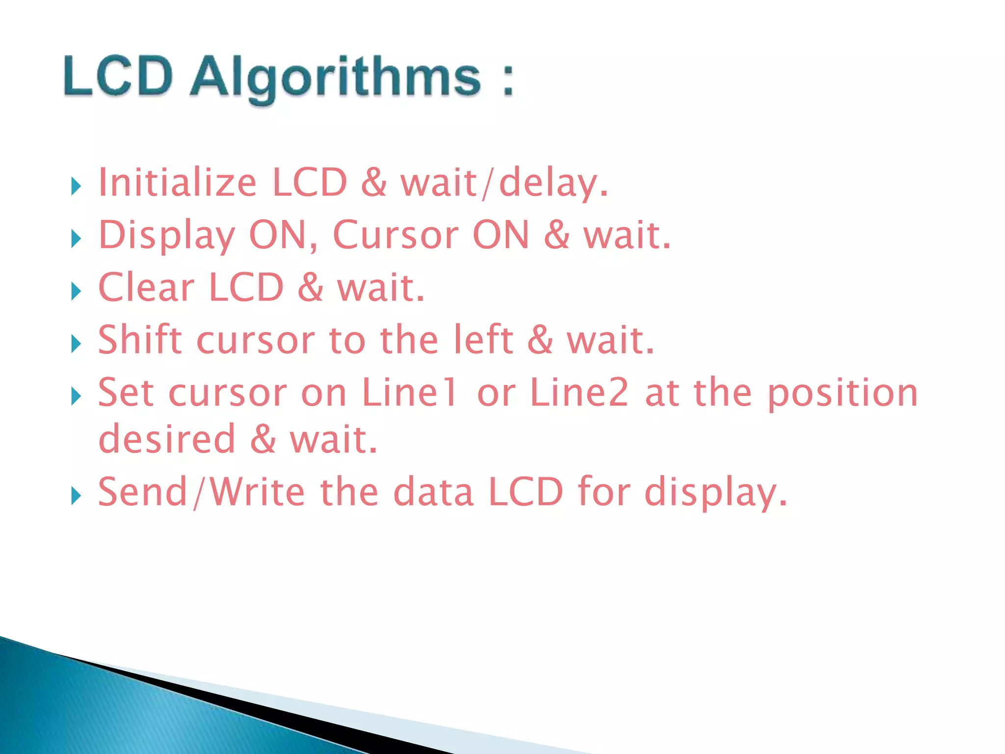
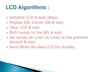
Initialize LCD& wait/delay.
Display ON, Cursor ON & wait.
Clear LCD & wait.
Shift cursor to the left & wait.
Set cursor on Line1 or Line2 at the position
desired & wait.
Send/Write the data LCD for display.
58.
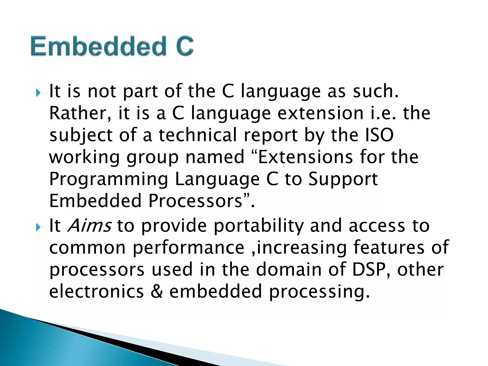
It isnot part of the C language as such.
Rather, it is a C language extension i.e. the
subject of a technical report by the ISO
working group named “Extensions for the
Programming Language C to Support
Embedded Processors”.
It Aims to provide portability and access to
common performance ,increasing features of
processors used in the domain of DSP, other
electronics & embedded processing.
59.
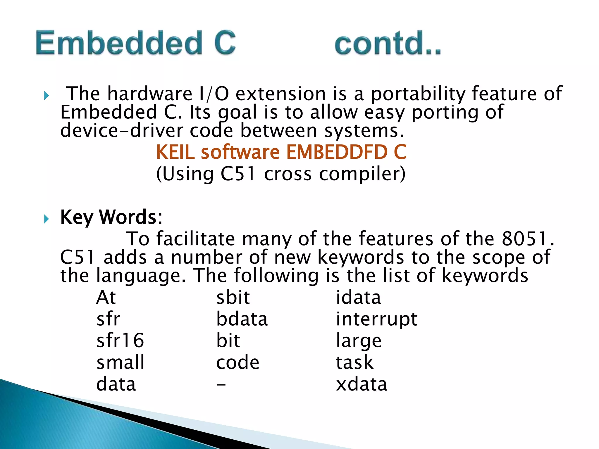
The hardwareI/O extension is a portability feature of
Embedded C. Its goal is to allow easy porting of
device-driver code between systems.
KEIL software EMBEDDFD C
(Using C51 cross compiler)
Key Words:
To facilitate many of the features of the 8051.
C51 adds a number of new keywords to the scope of
the language. The following is the list of keywords
At sbit idata
sfr bdata interrupt
sfr16 bit large
small code task
data - xdata
60.
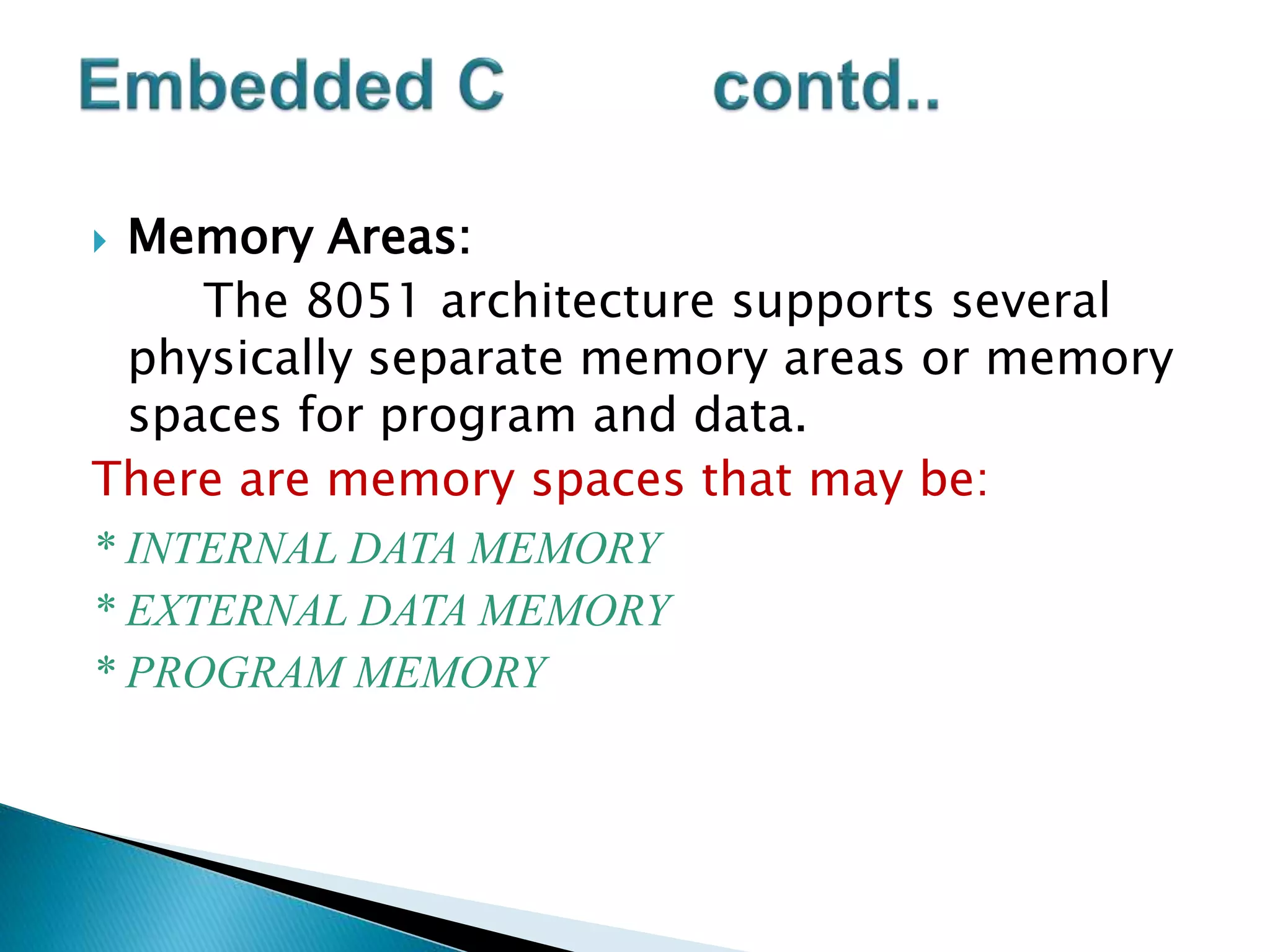
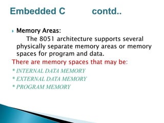
Memory Areas:
The8051 architecture supports several
physically separate memory areas or memory
spaces for program and data.
There are memory spaces that may be:
* INTERNAL DATA MEMORY
* EXTERNAL DATA MEMORY
* PROGRAM MEMORY
61.
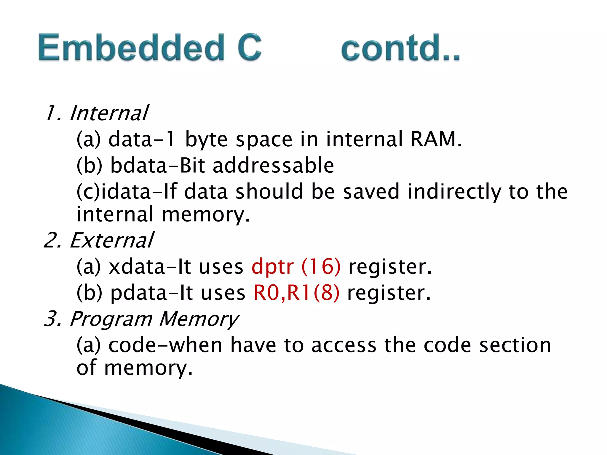
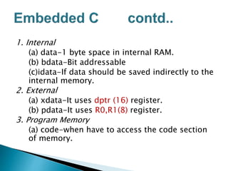
1. Internal
(a) data-1byte space in internal RAM.
(b) bdata-Bit addressable
(c)idata-If data should be saved indirectly to the
internal memory.
2. External
(a) xdata-It uses dptr (16) register.
(b) pdata-It uses R0,R1(8) register.
3. Program Memory
(a) code-when have to access the code section
of memory.
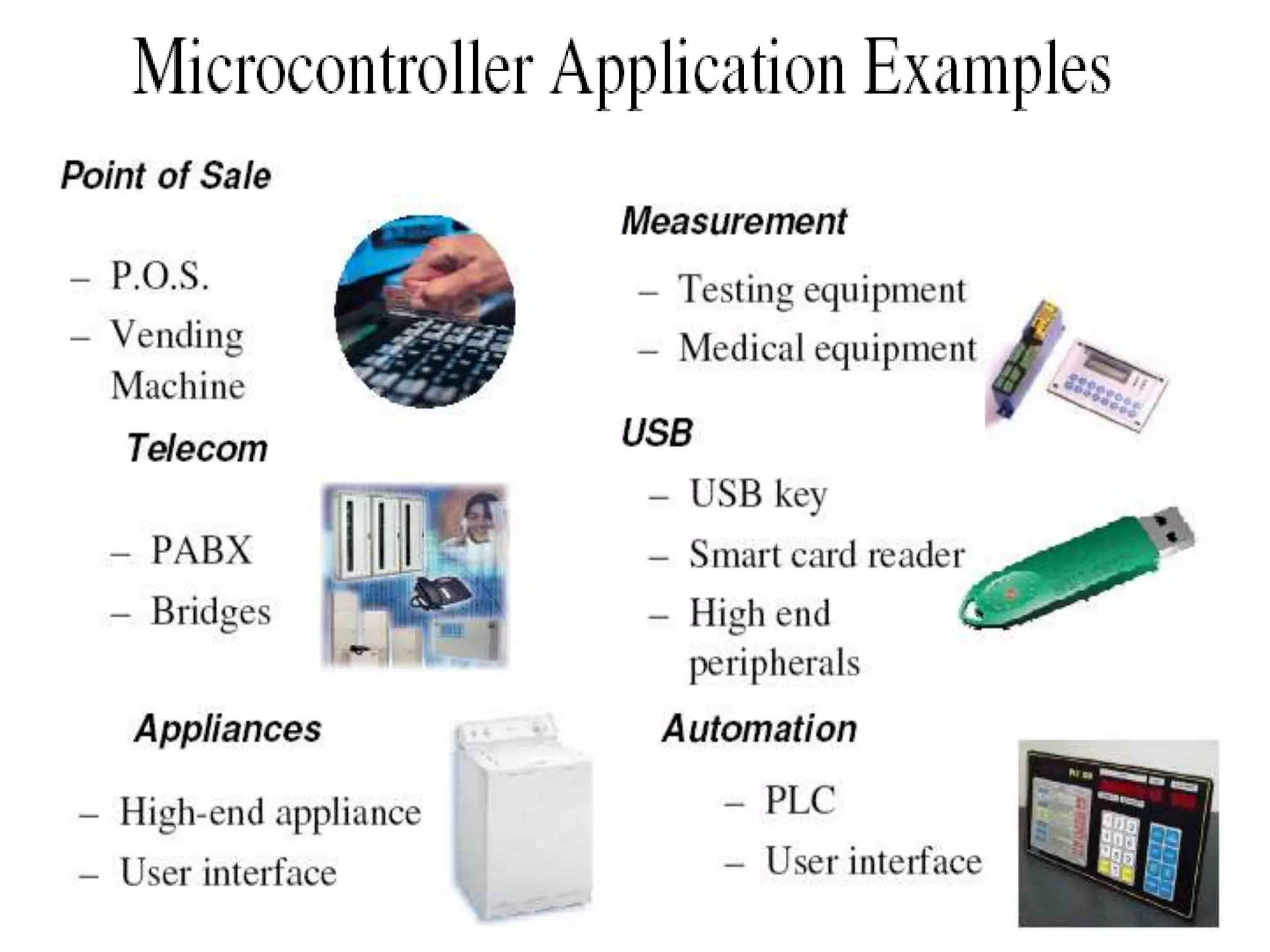
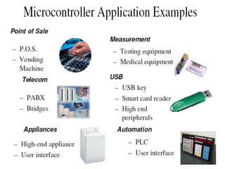
Its notan exaggeration if I say that ,today
there is no electronic gadget on the earth
which is designed without a Microcontroller.
Ex: communication devices, digital
entertainment, portable devices etc.


![ Four banks of 8 byte-sized registers, R0 to R7
Addresses are :
18 - 1F for bank 3
10 - 17 for bank 2
08 - 0F for bank 1
00 - 07 for bank 0 (default)
Active bank selected by bits [ RS1, RS0 ] in
PSW.
Permits fast “context switching” in interrupt
service routines (ISR).](https://image.slidesharecdn.com/007-151009160515-lva1-app6891/85/Presentation-On-Micro-controller-8051-Embedded-System-33-320.jpg)


![ Four banks of 8 byte-sized registers, R0 to R7
Addresses are :
18 - 1F for bank 3
10 - 17 for bank 2
08 - 0F for bank 1
00 - 07 for bank 0 (default)
Active bank selected by bits [ RS1, RS0 ] in
PSW.
Permits fast “context switching” in interrupt
service routines (ISR).](https://image.slidesharecdn.com/007-151009160515-lva1-app6891/75/Presentation-On-Micro-controller-8051-Embedded-System-33-2048.jpg)