Downloaded 498 times


Programmable logic devices (PLDs) like PLA, PAL, CPLD and FPGA allow implementing logic circuits using programmable switches. PLA and PAL have programmable AND planes and OR planes to implement sum-of-products logic. PALs are simpler than PLAs with fixed OR planes. CPLDs contain multiple PAL-like blocks with programmable interconnects. FPGAs provide programmable logic blocks and interconnects to implement larger circuits without AND/OR planes. All PLDs require programming using CAD tools to set the switches for the desired logic function.
Overview of presentation focusing on Programmable Array Logic with presenters listed.
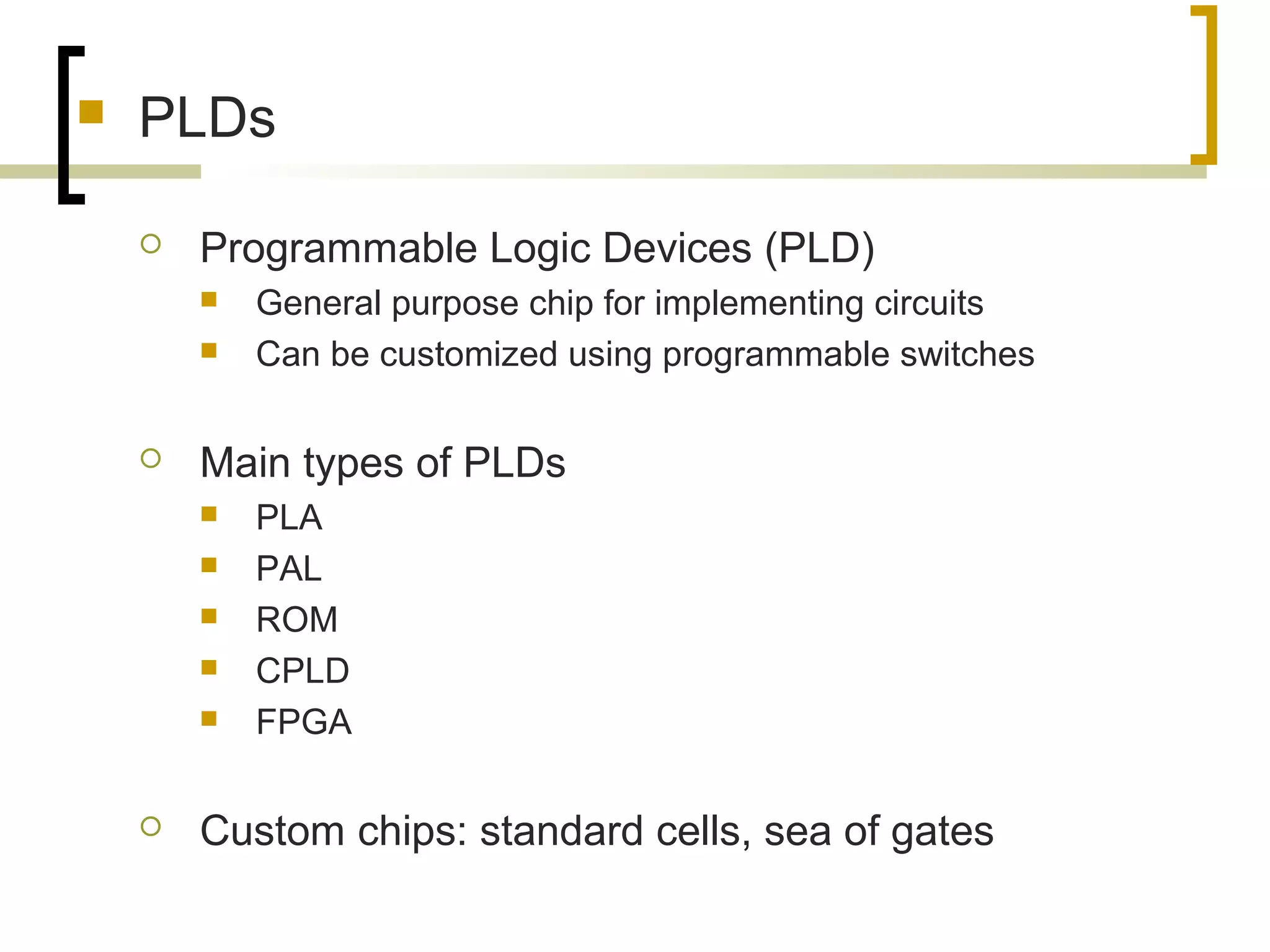
Discussion on Programmable Logic Devices (PLDs), their customization and main types: PLA, PAL, ROM, CPLD, FPGA.
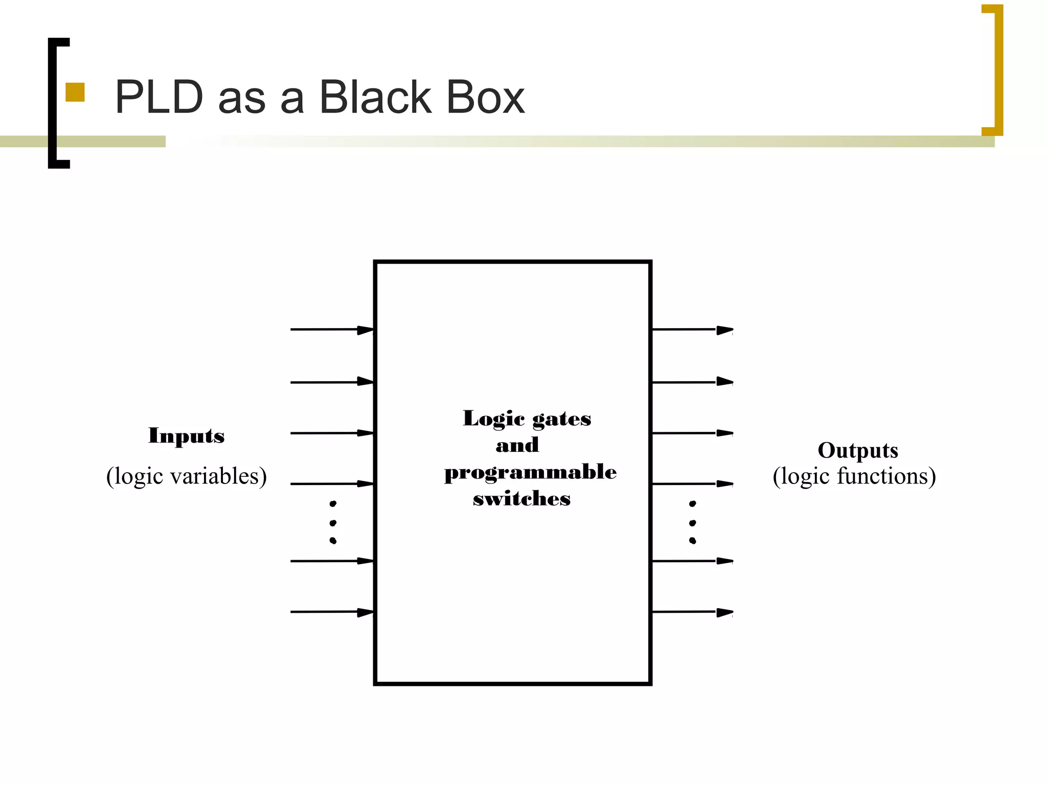
Illustration of PLDs as black boxes with inputs as logic variables and outputs as logic functions.
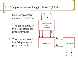
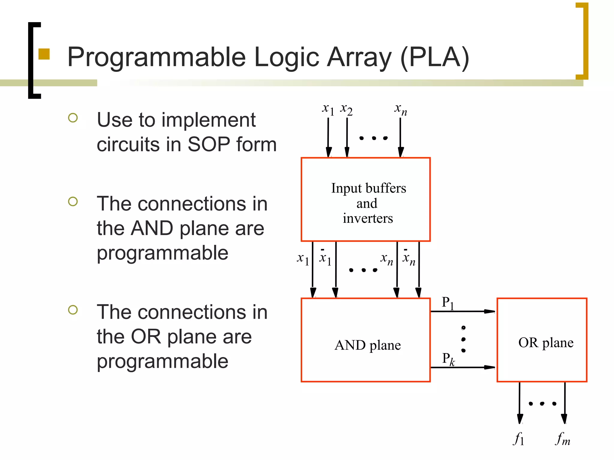
Description of PLA usage for circuits in SOP form, with programmable connections in AND and OR planes.
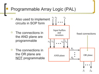
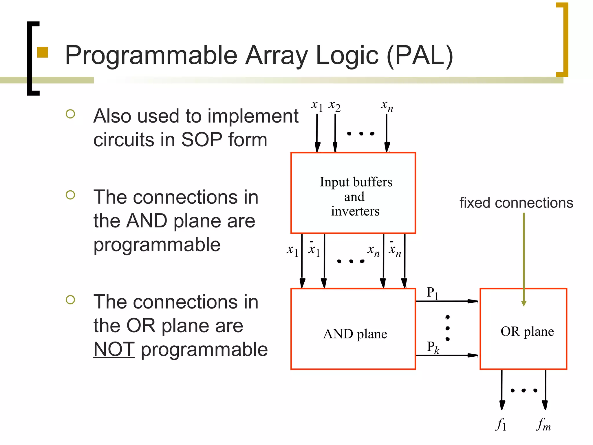
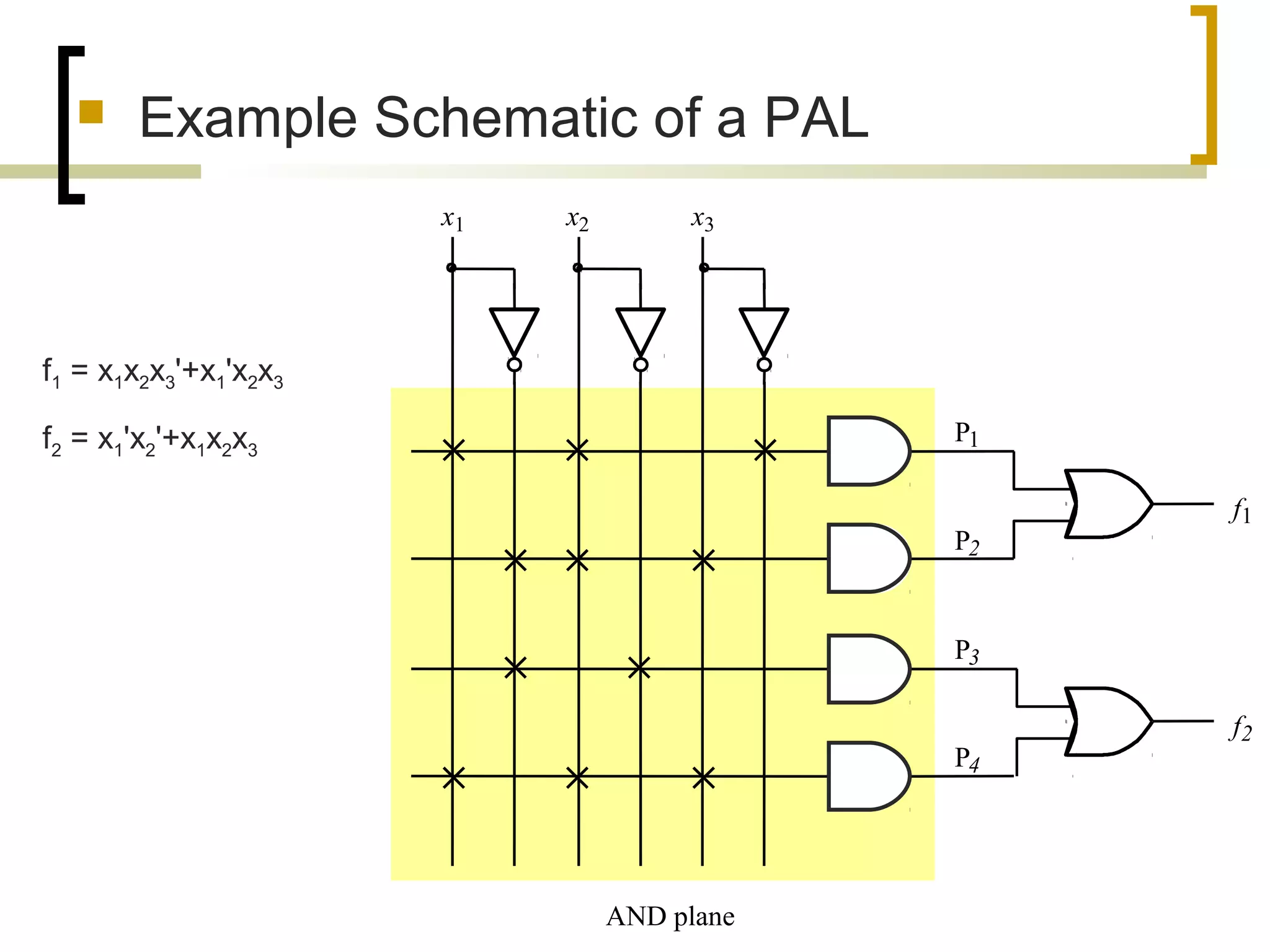
Outline of PAL’s use in SOP circuits, highlighting programmable AND plane and fixed OR plane connections.
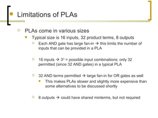
Discusses PLA limitations, including size, input/output constraints, and performance considerations.
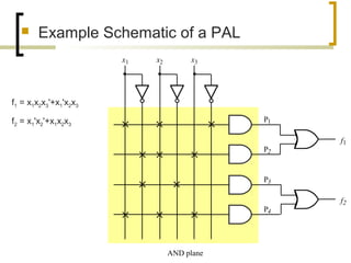
A schematic example illustrating functions and connections in a PAL setup.
Comparison highlighting the limitations of PALs versus PLAs, including performance and complexity.
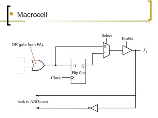
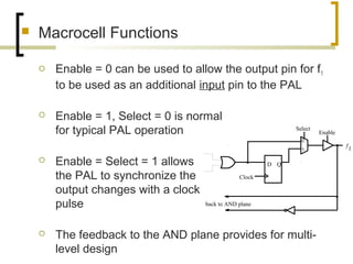
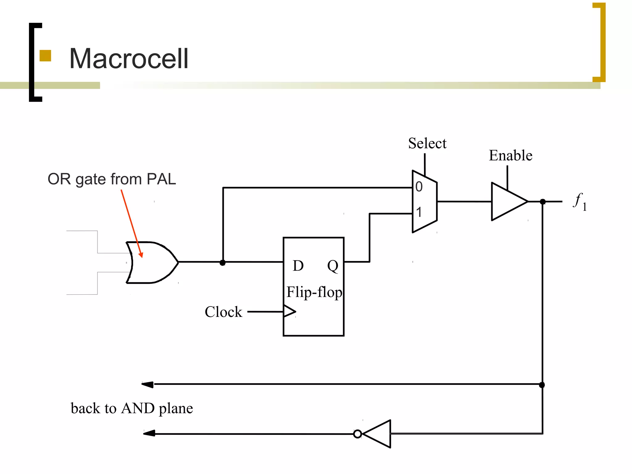
Definition and role of macrocells in PAL, including feedback and clock synchronization.
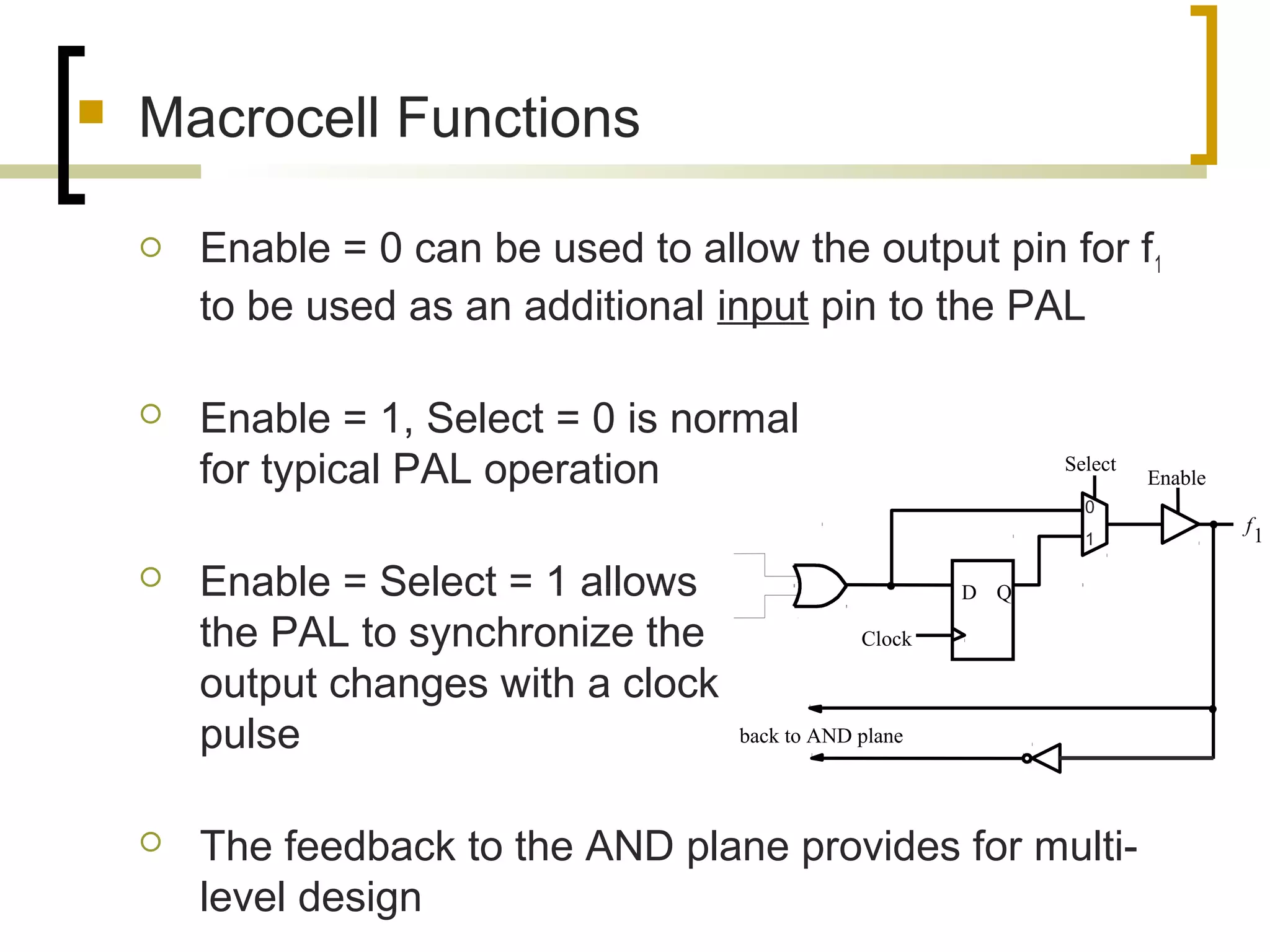
Detailed functionality of macrocells, including output functionality and design synchronization.
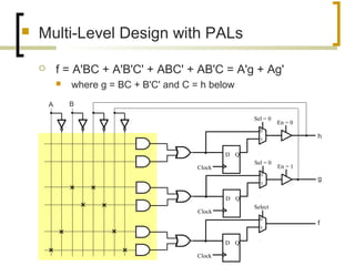
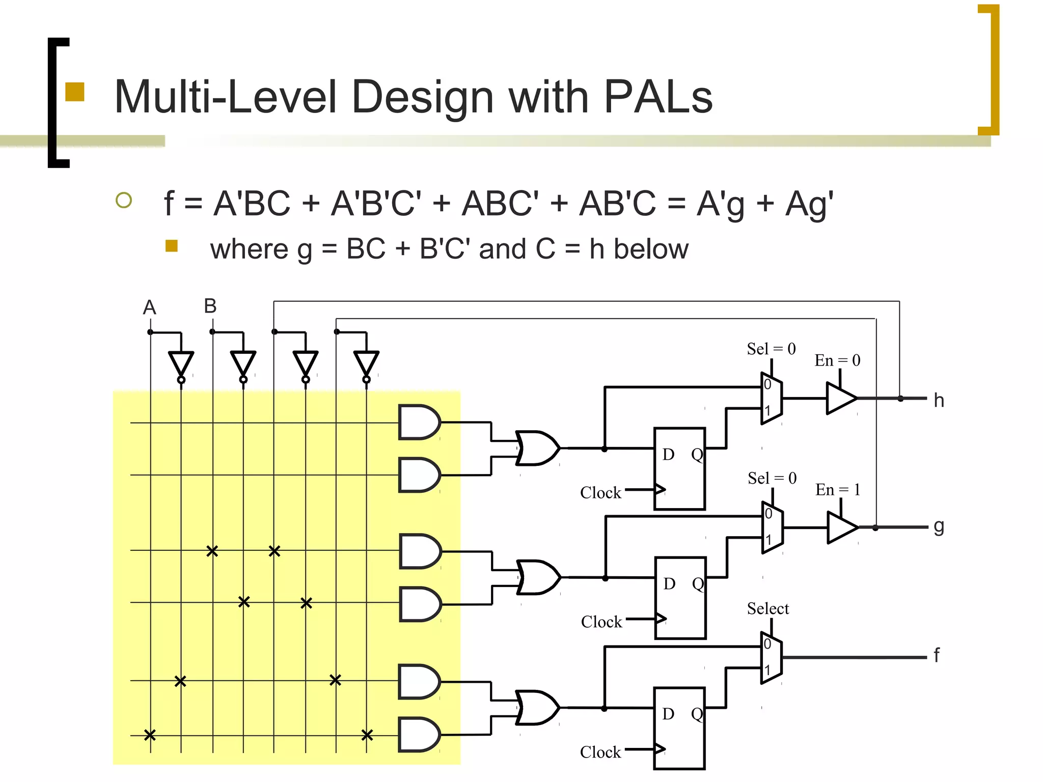
Explains multi-level design using PALs for logic functions through a detailed mathematical expression.
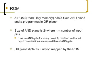
Overview of ROM with fixed AND plane and programmable OR plane for decoding logic combinations.
Methods to program SPLDs (PLAs, PALs, ROMs) with CAD tools and fuse map usage for programming.
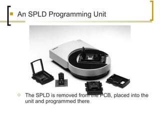
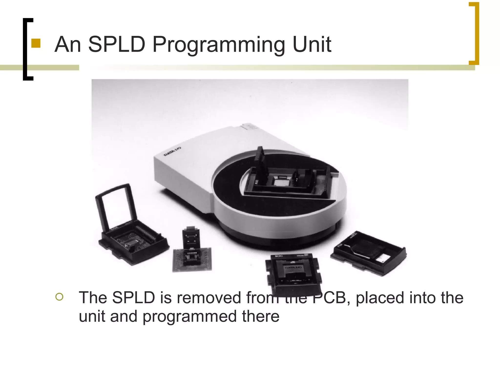
Description of the SPLD programming unit for programming devices outside of the PCB.
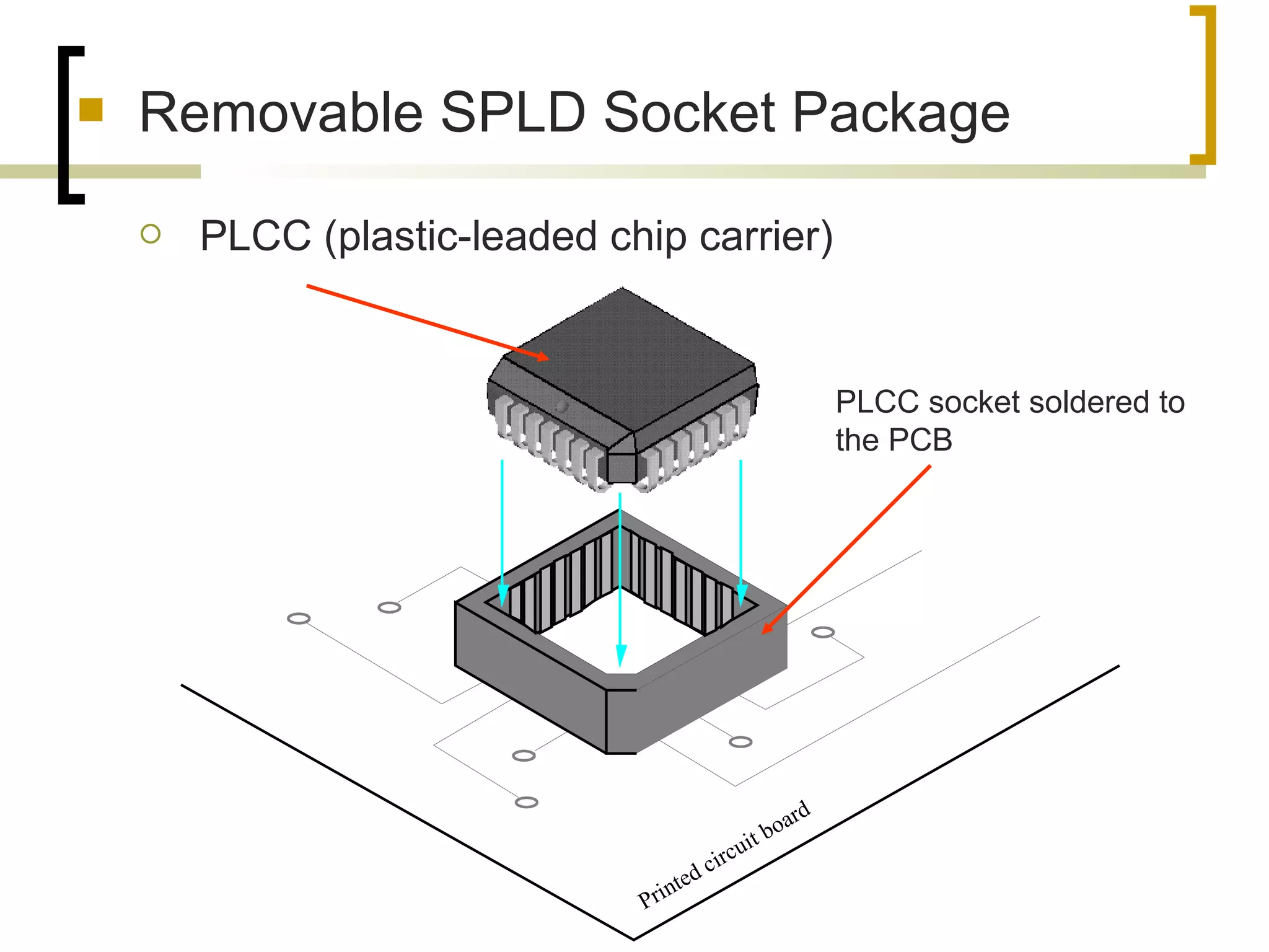
Introduction to removable SPLD socket packages, specifically PLCC for ease of integration.
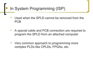
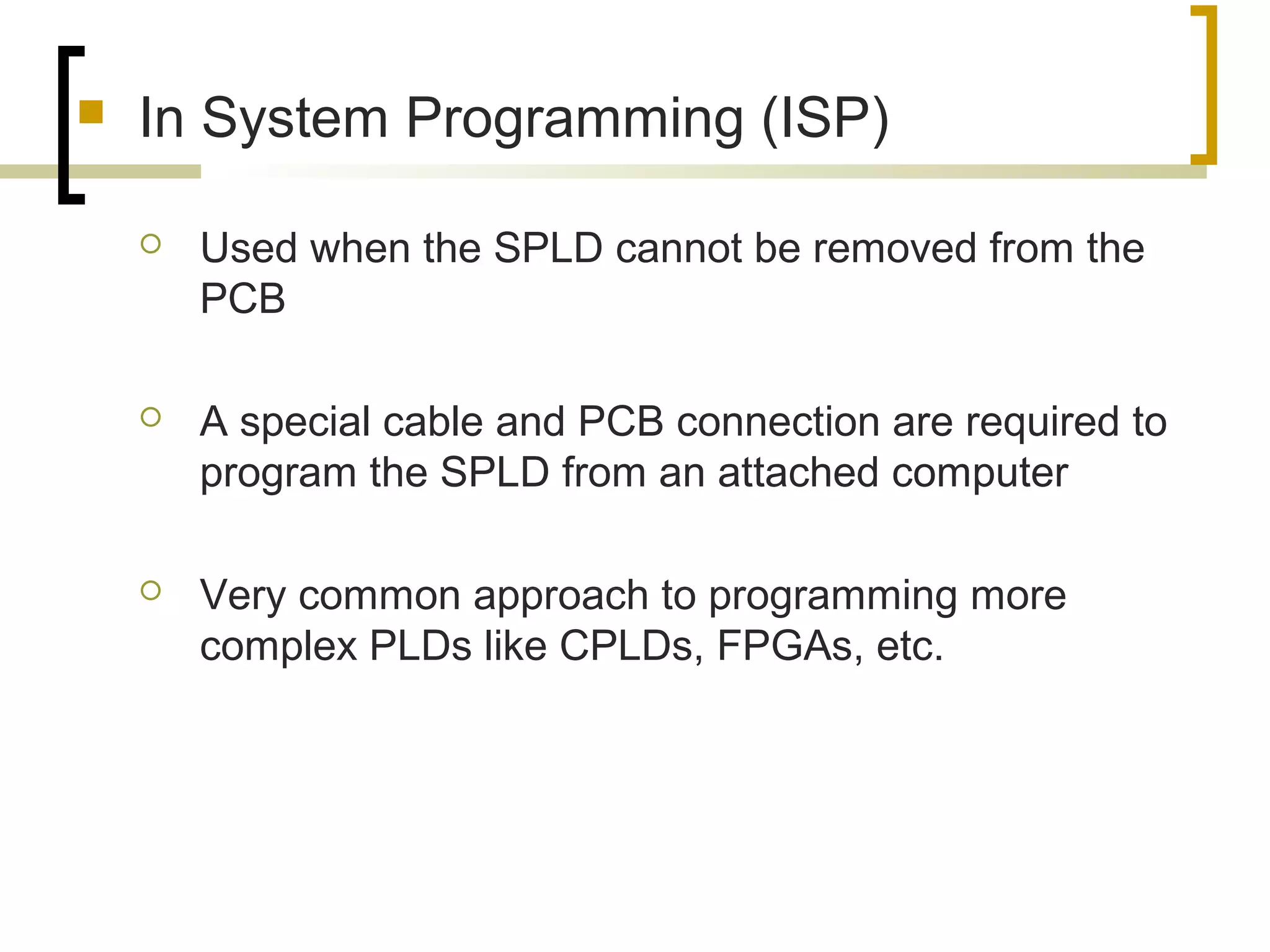
Details of ISP for non-removable SPLDs programming using a special cable and computer interface.
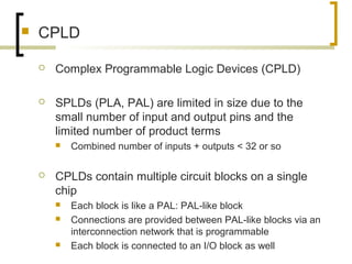
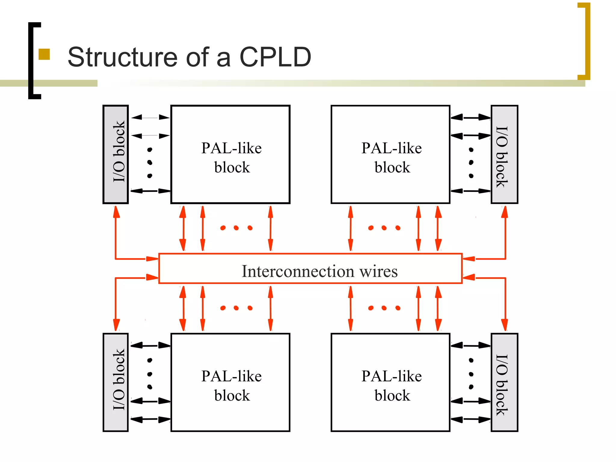
Overview of Complex Programmable Logic Devices (CPLDs), highlighting their structure and capabilities.
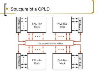
Illustration of CPLD structure including multiple PAL-like blocks and interconnection networks.
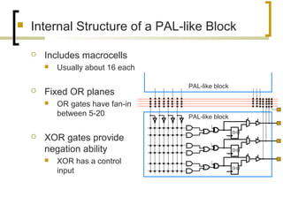
Detail on PAL-like blocks within CPLDs, including macrocells and fixed OR planes.
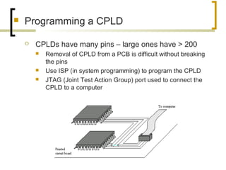
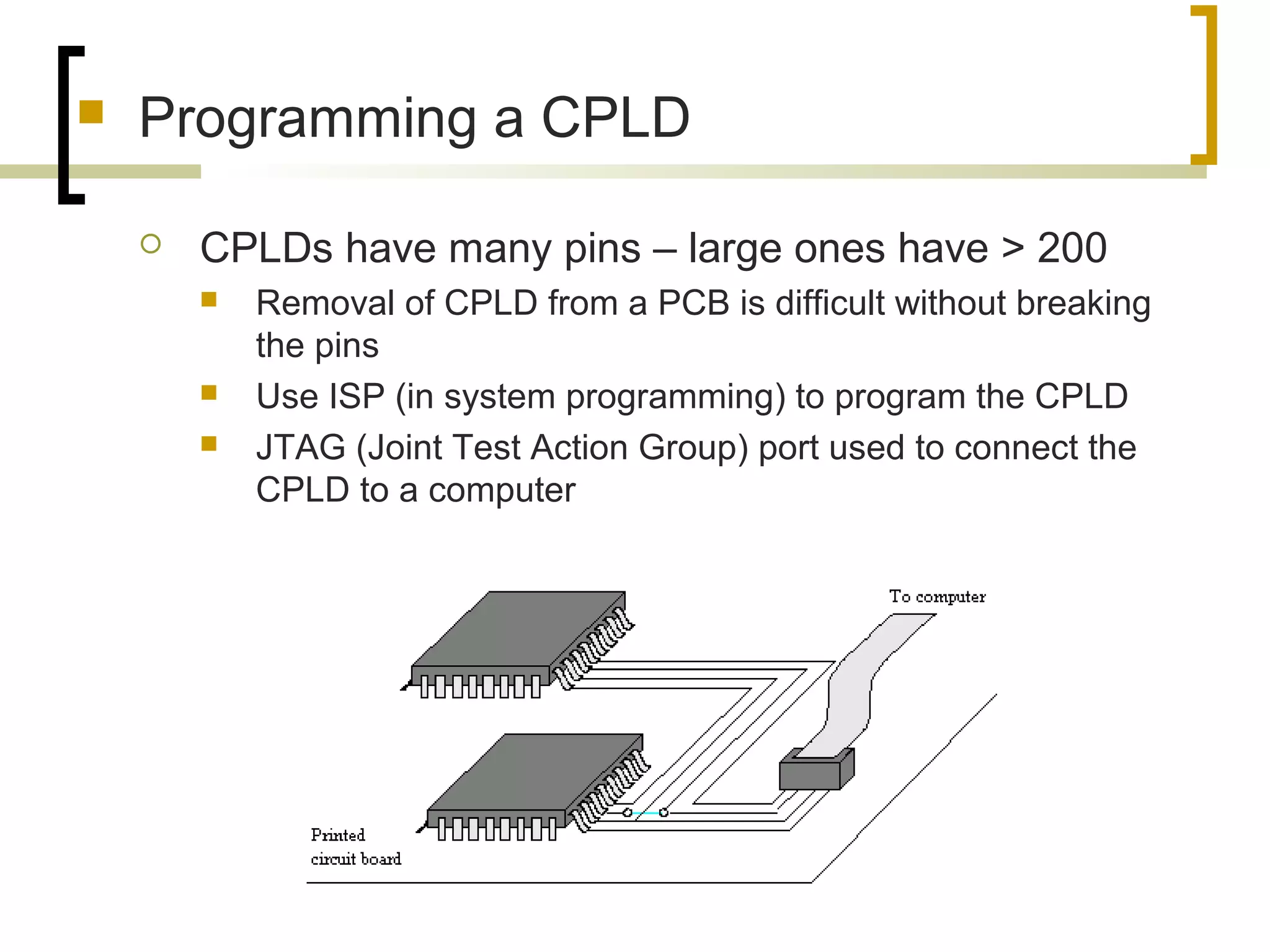
Information on programming methods for CPLDs, focusing on ISP and JTAG connections.
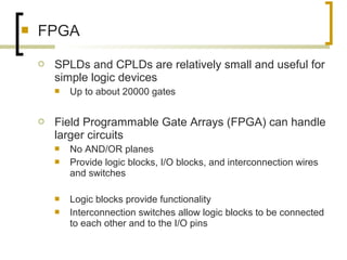
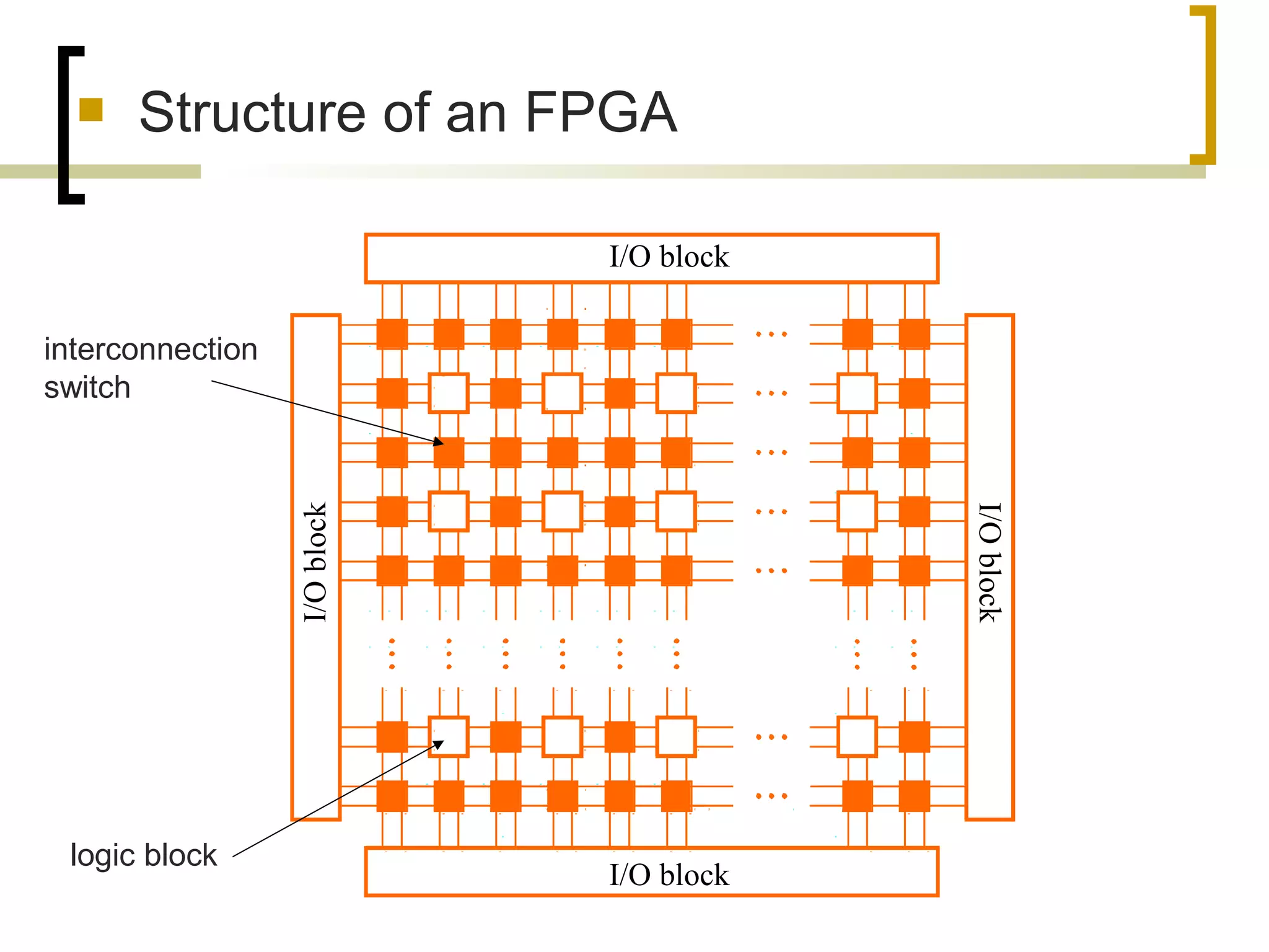
Description of FPGAs, highlighting their ability to handle larger circuits without AND/OR planes.
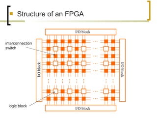
Diagrammatic representation of FPGA structure featuring I/O blocks and logic blocks.
Ending remarks and thank you note to the audience.


