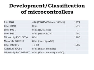
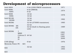
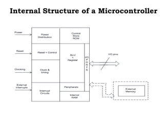
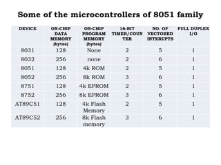
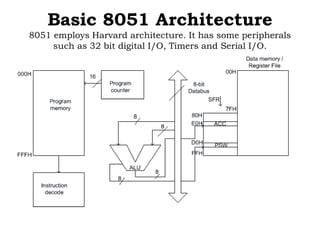
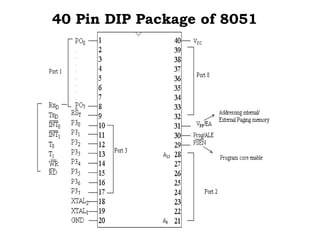
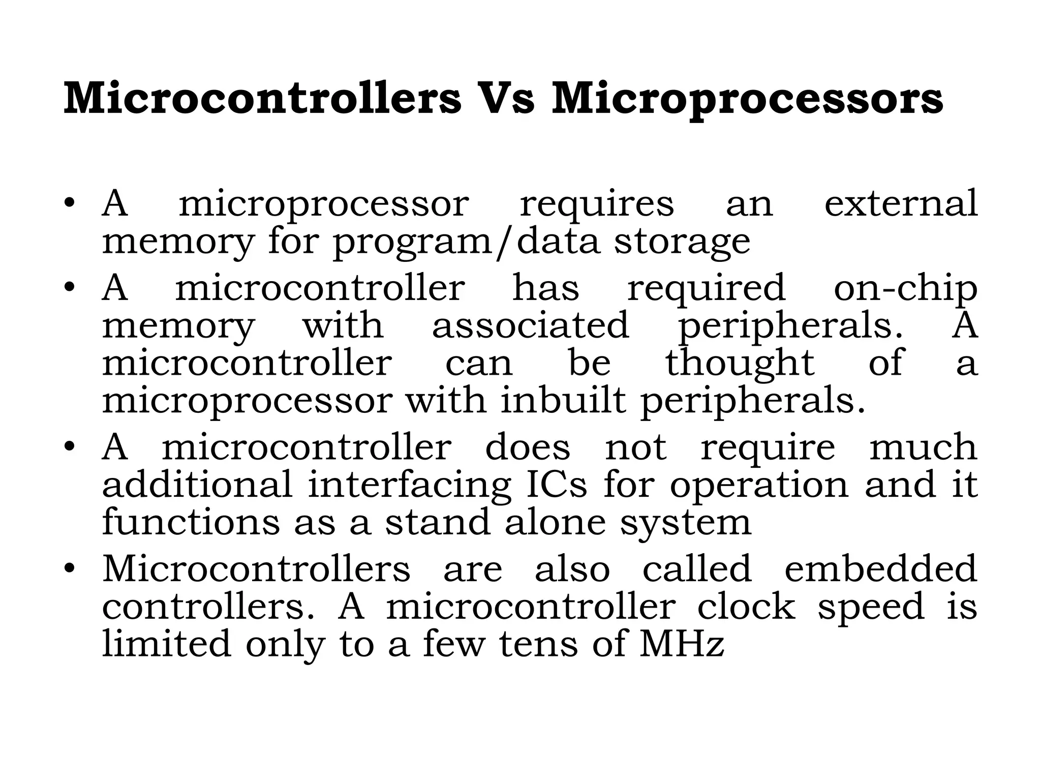
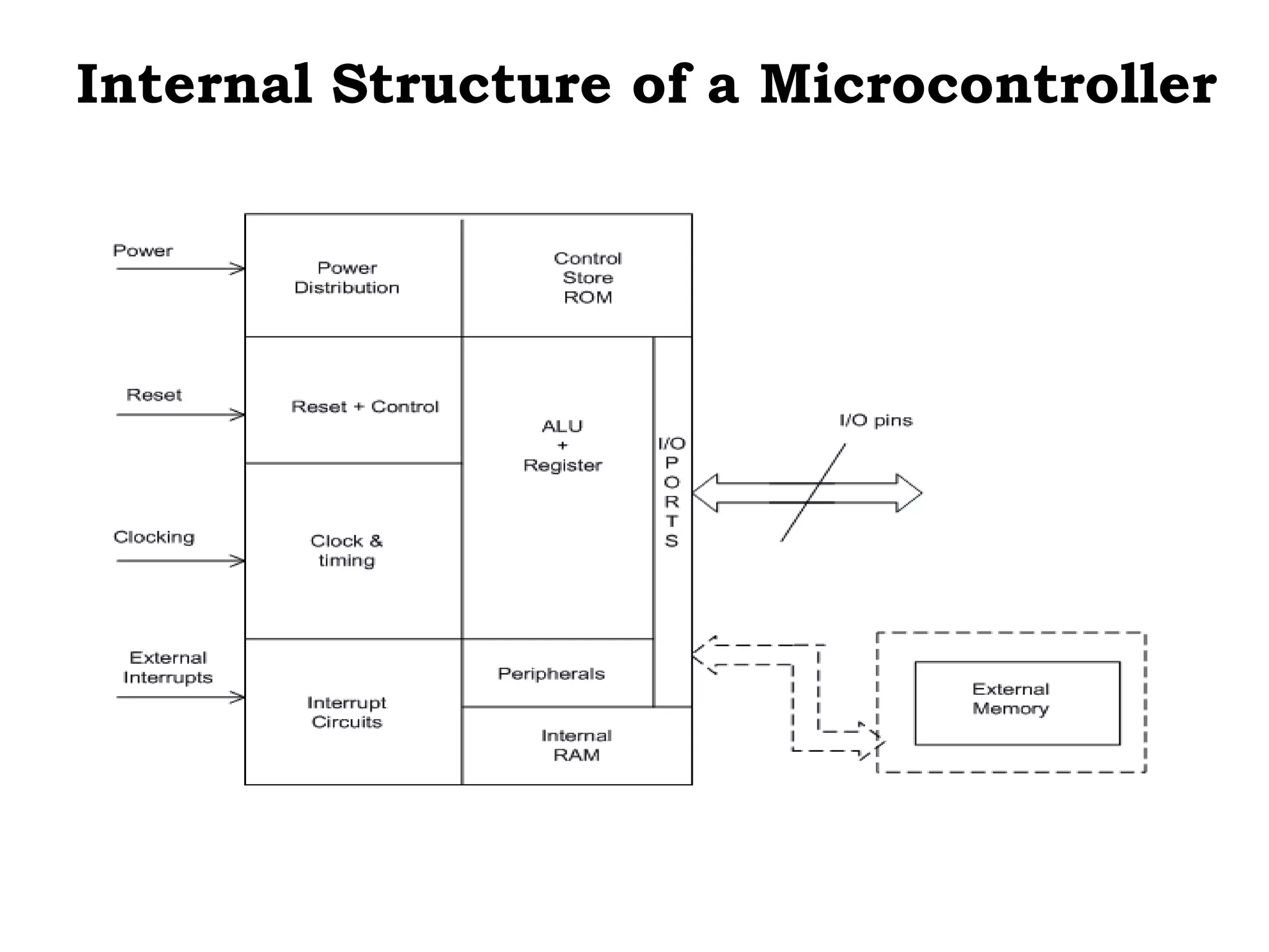
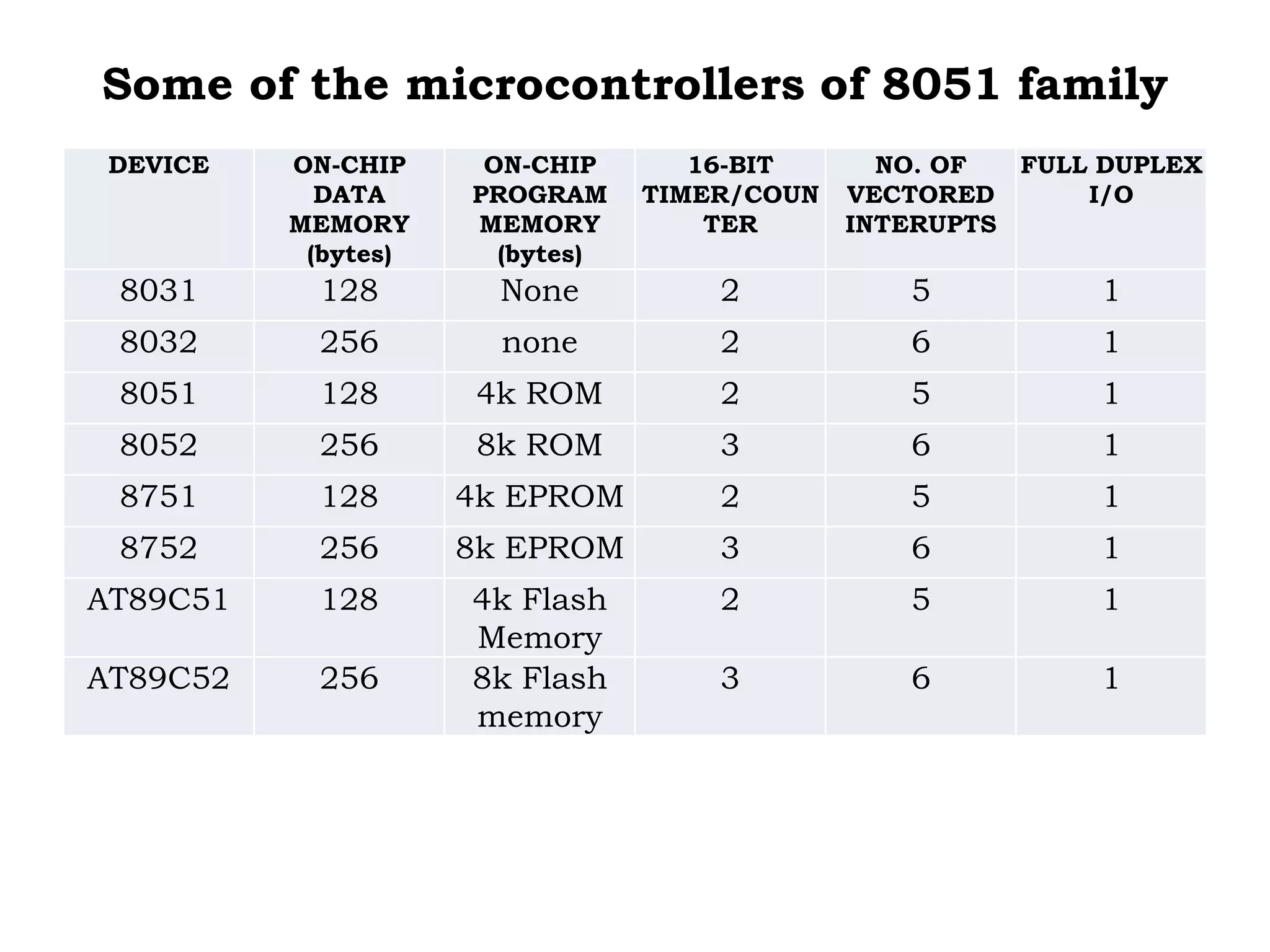
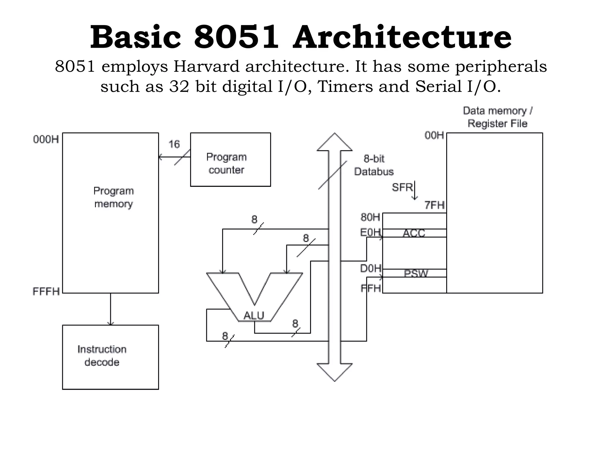
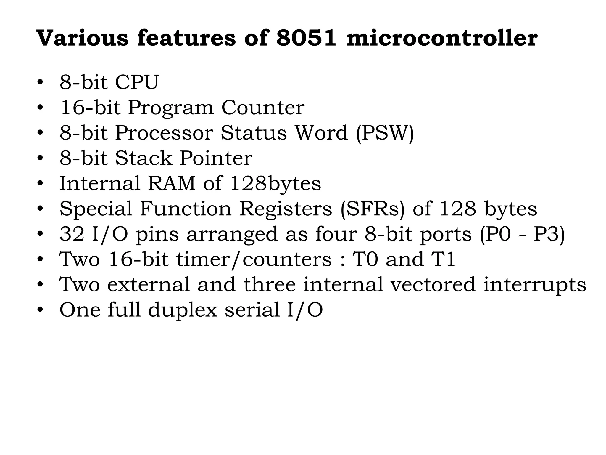
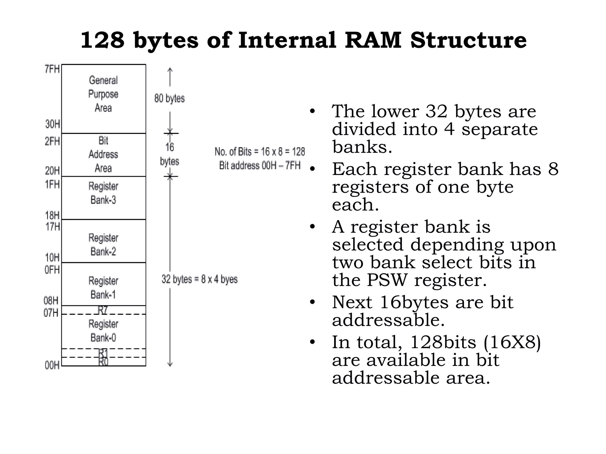
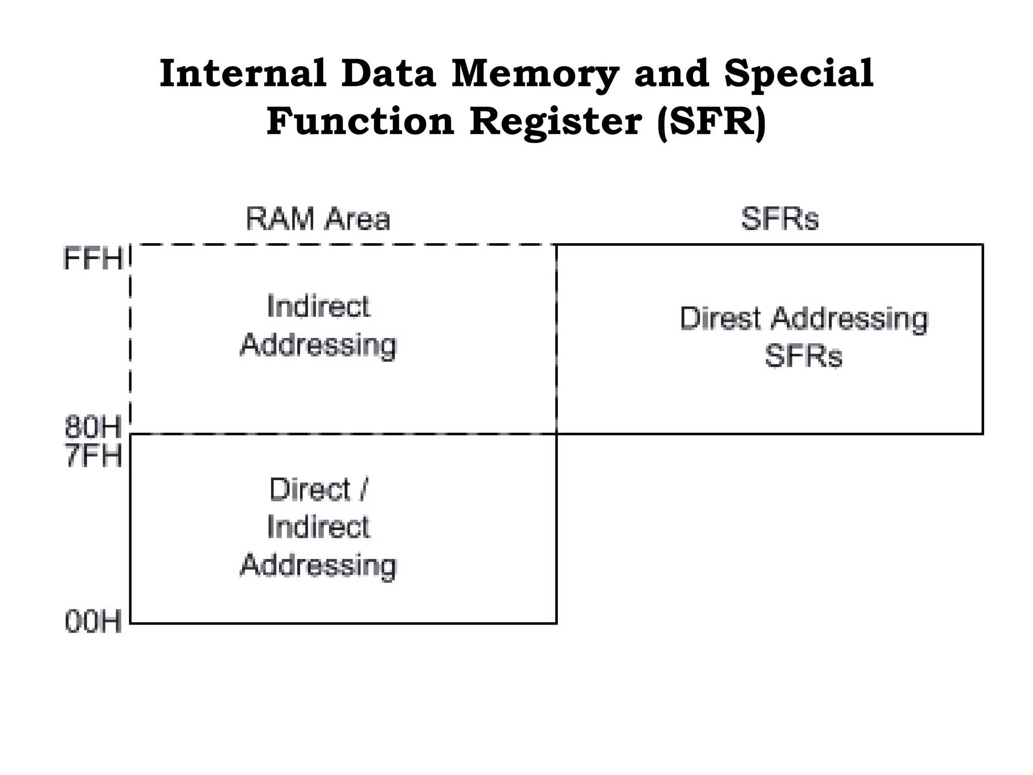
KEMBAR78
Unit iv introduction to 8051 microcontroller ppts | PPTX
UNIT-IV
Introduction to 8051
Microcontroller
A Microcontroller is a programmable
digital processor with necessary peripherals.
Both microcontrollers and microprocessors
are complex sequential digital circuits meant to
carry out job according to the program /
instructions.
Microcontrollers Vs Microprocessors
• A microprocessor requires an external
memory for program/data storage
• A microcontroller has required on-chip
memory with associated peripherals. A
microcontroller can be thought of a
microprocessor with inbuilt peripherals.
• A microcontroller does not require much
additional interfacing ICs for operation and it
functions as a stand alone system
• Microcontrollers are also called embedded
controllers. A microcontroller clock speed is
limited only to a few tens of MHz
Development/Classification
of microcontrollers
Intel4004 4 bit (2300 PMOS trans, 108 kHz) 1971
Intel 8048 8 bit 1976
Intel 8031 8 bit (ROM-less) .
Intel 8051 8 bit (Mask ROM) 1980
Microchip PIC16C64 8 bit 1985
Motorola 68HC11 8 bit (on chip ADC) .
Intel 80C196 16 bit 1982
Atmel AT89C51 8 bit (Flash memory) .
Microchip PIC 16F877 8 bit (Flash memory + ADC) .
Development of microprocessors
Intel 4004 4 bit (2300 PMOS transistors) 1971
Intel 8080
8085
8 bit (NMOS)
8 bit
1974
Intel 8088
8086
16 bit
16 bit
1978
Intel 80186
80286
16 bit
16 bit
1982
Intel 80386 32 bit (275000 transistors) 1985
Intel 80486 SX
DX
32 bit
32 bit (built in floating point
unit)
1989
Intel 80586 I
MMX
Celeron II
III
IV
64 bit
1993
1997
1999
2000
Z-80 (Zilog) 8 bit 1976
Motorola Power PC 601
602
603
32-bit 1993
1995
Internal Structure of a Microcontroller
Some of the microcontrollers of 8051 family
DEVICE ON-CHIP
DATA
MEMORY
(bytes)
ON-CHIP
PROGRAM
MEMORY
(bytes)
16-BIT
TIMER/COUN
TER
NO. OF
VECTORED
INTERUPTS
FULL DUPLEX
I/O
8031 128 None 2 5 1
8032 256 none 2 6 1
8051 128 4k ROM 2 5 1
8052 256 8k ROM 3 6 1
8751 128 4k EPROM 2 5 1
8752 256 8k EPROM 3 6 1
AT89C51 128 4k Flash
Memory
2 5 1
AT89C52 256 8k Flash
memory
3 6 1
Basic 8051 Architecture
8051 employs Harvard architecture. It has some peripherals
such as 32 bit digital I/O, Timers and Serial I/O.
40 Pin DIP Package of 8051
Various features of 8051 microcontroller
• 8-bit CPU
• 16-bit Program Counter
• 8-bit Processor Status Word (PSW)
• 8-bit Stack Pointer
• Internal RAM of 128bytes
• Special Function Registers (SFRs) of 128 bytes
• 32 I/O pins arranged as four 8-bit ports (P0 - P3)
• Two 16-bit timer/counters : T0 and T1
• Two external and three internal vectored interrupts
• One full duplex serial I/O
128 bytes of Internal RAM Structure
• The lower 32 bytes are
divided into 4 separate
banks.
• Each register bank has 8
registers of one byte
each.
• A register bank is
selected depending upon
two bank select bits in
the PSW register.
• Next 16bytes are bit
addressable.
• In total, 128bits (16X8)
are available in bit
addressable area.
Internal Data Memory and Special
Function Register (SFR)
8051 Addressing Modes
8051 has four addressing modes.
1. Immediate Addressing :
Data is immediately available in the instruction.
For example -
ADD A, #77; Adds 77 (decimal) to A and stores in A
ADD A, #4DH; Adds 4D (hexadecimal) to A and stores in A
MOV DPTR, #1000H; Moves 1000 (hexadecimal) to data pointer
2. Bank Addressing or Register Addressing :
This way of addressing accesses the bytes in the current register bank.
Data is available in the register specified in the instruction. The
register bank is decided by 2 bits of Processor Status Word (PSW).
For example-
ADD A, R0; Adds content of R0 to A and stores in A
3.. Direct Addressing :
The address of the data is available in the instruction.
For example -
MOV A, 088H; Moves content of SFR TCON (address 088H)to A
Contd…….
4. Register Indirect Addressing :
The address of data is available in the R0 or R1 registers as specified in the instruction.
For example -
MOV A, @R0 moves content of address pointed by R0 to A
External Data Addressing :
Pointer used for external data addressing can be either R0/R1 (256 byte access) or DPTR
(64kbyte access).
For example -
MOVX A, @R0; Moves content of 8-bit address pointed by R0 to A
MOVX A, @DPTR; Moves content of 16-bit address pointed by DPTR to A
External Code Addressing :
Sometimes we may want to store non-volatile data into the ROM e.g. look-up tables. Such
data may require reading the code memory. This may be done as follows -
MOVC A, @A+DPTR; Moves content of address pointed by A+DPTR to A
MOVC A, @A+PC; Moves content of address pointed by A+PC to A
I/O Port Configuration
Each port of 8051 has
bidirectional capability.
Port 0 is called 'true
bidirectional port' as it floats
(tristated) when configured as
input.
Port-1, 2, 3 are called 'quasi
bidirectional port'.
PORT-0 PIN Structure:
Port -0 has 8 pins (P0.0-P0.7)
Port-1 Pin Structure
• Port-1 has 8 pins (P1.1-P1.7) it is dedicated solely for I/O
interfacing
PORT 2 Pin Structure
Port-2 has 8-pins (P2.0-P2.7) Port-2 is used for higher external address
byte or a normal input/output port .
P3.0 RxD
P3.1 TxD
P3.2 INT0’
P3.3 INT1’
P3.4 T0
P3.5 T1
P3.6 WR’
P3.7 RD’
PORT 3 Pin Structure
Port-3 has 8 pin (P3.0-P3.7) Each pin of Port-3 can be individually
programmed for I/O operation or for alternate function
Note:
1.Port 1, 2, 3 each can drive 4 LS TTL
inputs.
2.Port-0 can drive 8 LS TTL inputs in
address /data mode. For digital output
port, it needs external pull-up resistors.
3.Ports-1,2and 3 pins can also be driven
by open-collector or open-drain outputs.
4.Each Port 3 bit can be configured either
as a normal I/O or as a special function
bit.
Accessing external memory
Access to external program memory uses the signal (Program store enable) as the read strobe. Access to external data memory
uses (alternate function of P3.7 and P3.6).
For external program memory, always 16 bit address is used. For example -
MOVC A, @ A+DPTR
MOVC A, @ A+PC
Access to external data memory can be either 8-bit address or 16-bit address -
8-bit address- MOVX A, @Rp where Rp is either R0 or R1
MOVX @Rp, A
16 bit address- MOVX A,@DPTR
MOV X @DPTR, A
8051 Instructions
8051 has about 111 instructions. These can be grouped into the following categories
1.Arithmetic Instructions
2.Logical Instructions
3.Data Transfer instructions
4.Boolean Variable Instructions
5.Program Branching Instructions
The following nomenclatures for register, data, address and variables are used while write
instructions.
A: Accumulator
B: "B" register
C: Carry bit
Rn: Register R0 - R7 of the currently selected register bank
Direct: 8-bit internal direct address for data. The data could be in lower 128bytes of RAM
(00 - 7FH) or it could be in the special function register (80 - FFH).
@Ri: 8-bit external or internal RAM address available in register R0 or R1. This is used for
indirect addressing mode.
#data8: Immediate 8-bit data available in the instruction.
#data16: Immediate 16-bit data available in the instruction.
Addr11: 11-bit destination address for short absolute jump. Used by instruction AJMP &
ACALL Jump range is 2 kbyte (one page).
Addr16: 16-bit destination address for long call or long jump.
Rel: 2's complement 8-bit offset (one - byte) used for short jump (SJMP) and all conditional
jumps.
bit: Directly addressed bit in internal RAM or SFR
Mnemonics Description Bytes Instruction Cycles
ADD A, Rn A A + Rn 1 1
ADD A, direct A A + (direct) 2 1
ADD A, @Ri A A + @Ri 1 1
ADD A, #data A A + data 2 1
ADDC A, Rn A A + Rn + C 1 1
ADDC A, direct A A + (direct) + C 2 1
ADDC A, @Ri A A + @Ri + C 1 1
ADDC A, #data A A + data + C 2 1
DA A Decimal adjust accumulator 1 1
DIV AB Divide A by B A quotient
B remainder
1 4
DEC A A A -1 1 1
DEC Rn Rn Rn - 1 1 1
DEC direct (direct) (direct) - 1 2 1
DEC @Ri @Ri @Ri - 1 1 1
INC A A A+1 1 1
INC Rn Rn Rn + 1 1 1
INC direct (direct) (direct) + 1 2 1
INC @Ri @Ri @Ri +1 1 1
INC DPTR DPTR DPTR +1 1 2
MUL AB Multiply A by B A low byte (A*B)
B high byte (A*
B)
1 4
SUBB A, Rn A A - Rn - C 1 1
SUBB A, direct A A - (direct) - C 2 1
SUBB A, @Ri A A - @Ri - C 1 1
SUBB A, #data A A - data - C 2 1
Arithmetic Instructions:
Mnemonics Description Bytes Instruction Cycles
ANL A, Rn A A AND Rn 1 1
ANL A, direct A A AND (direct) 2 1
ANL A, @Ri A A AND @Ri 1 1
ANL A, #data A A AND data 2 1
ANL direct, A (direct) (direct) AND A 2 1
ANL direct, #data (direct) (direct) AND data 3 2
CLR A A 00H 1 1
CPL A AA 1 1
ORL A, Rn A A OR Rn 1 1
ORL A, direct A A OR (direct) 1 1
ORL A, @Ri A A OR @Ri 2 1
ORL A, #data A A OR data 1 1
ORL direct, A (direct) (direct) OR A 2 1
ORL direct, #data (direct) (direct) OR data 3 2
RL A Rotate accumulator left 1 1
RLC A Rotate accumulator left through carry 1 1
RR A Rotate accumulator right 1 1
RRC A Rotate accumulator right through carry 1 1
SWAP A Swap nibbles within Acumulator 1 1
XRL A, Rn A A EXOR Rn 1 1
XRL A, direct A A EXOR (direct) 1 1
XRL A, @Ri A A EXOR @Ri 2 1
XRL A, #data A A EXOR data 1 1
XRL direct, A (direct) (direct) EXOR A 2 1
Logical Instructions:
Mnemonics Description Bytes Instruction Cycles
MOV A, Rn A Rn 1 1
MOV A, direct A (direct) 2 1
MOV A, @Ri A @Ri 1 1
MOV A, #data A data 2 1
MOV Rn, A Rn A 1 1
MOV Rn, direct Rn (direct) 2 2
MOV Rn, #data Rn data 2 1
MOV direct, A (direct) A 2 1
MOV direct, Rn (direct) Rn 2 2
MOV direct1, direct2 (direct1) (direct2) 3 2
MOV direct, @Ri (direct) @Ri 2 2
MOV direct, #data (direct) #data 3 2
MOV @Ri, A @Ri A 1 1
MOV @Ri, direct @Ri (direct) 2 2
MOV @Ri, #data @Ri data 2 1
MOV DPTR, #data16 DPTR data16 3 2
MOVC A, @A+DPTR A Code byte pointed by A + DPTR 1 2
MOVC A, @A+PC A Code byte pointed by A + PC 1 2
MOVC A, @Ri A Code byte pointed by Ri 8-bit address) 1 2
MOVX A, @DPTR A External data pointed by DPTR 1 2
MOVX @Ri, A @Ri A (External data - 8bit address) 1 2
MOVX @DPTR, A @DPTR A(External data - 16bit address) 1 2
PUSH direct (SP) (direct) 2 2
POP direct (direct) (SP) 2 2
XCH Rn Exchange A with Rn 1 1
XCH direct Exchange A with direct byte 2 1
XCH @Ri Exchange A with indirect RAM 1 1
Data Transfer Instructions:
Mnemonics Description Bytes Instruction Cycles
CLR C C-bit 0 1 1
CLR bit bit 0 2 1
SET C C 1 1 1
SET bit bit 1 2 1
CPL C C 1 1
CPL bit bit 2 1
ANL C, /bit C C . 2 1
ANL C, bit C C. bit 2 1
ORL C, /bit C C + 2 1
ORL C, bit C C + bit 2 1
MOV C, bit C bit 2 1
MOV bit, C bit C 2 2
Boolean Variable Instructions:
Mnemonics Description Bytes Instruction Cycles
ACALL addr11 PC + 2 (SP) ; addr 11 PC 2 2
AJMP addr11 Addr11 PC 2 2
CJNE A, direct, rel Compare with A, jump (PC + rel) if not equal 3 2
CJNE A, #data, rel Compare with A, jump (PC + rel) if not equal 3 2
CJNE Rn, #data, rel Compare with Rn, jump (PC + rel) if not
equal
3 2
CJNE @Ri, #data, relCompare with @Ri A, jump (PC + rel) if not
equal
3 2
DJNZ Rn, rel Decrement Rn, jump if not zero 2 2
DJNZ direct, rel Decrement (direct), jump if not zero 3 2
JC rel Jump (PC + rel) if C bit = 1 2 2
JNC rel Jump (PC + rel) if C bit = 0 2 2
JB bit, rel Jump (PC + rel) if bit = 1 3 2
JNB bit, rel Jump (PC + rel) if bit = 0 3 2
JBC bit, rel Jump (PC + rel) if bit = 1 3 2
JMP @A+DPTR A+DPTR PC 1 2
JZ rel If A=0, jump to PC + rel 2 2
JNZ rel If A ≠ 0 , jump to PC + rel 2 2
LCALL addr16 PC + 3 (SP), addr16 PC 3 2
LJMP addr 16 Addr16 PC 3 2
RET (SP) PC 1 2
RETI (SP) PC, Enable Interrupt 1 2
SJMP rel PC + 2 + rel PC 2 2
JMP @A+DPTR A+DPTR PC 1 2
JZ rel If A = 0. jump PC+ rel 2 2
JNZ rel If A ≠ 0, jump PC + rel 2 2
NOP No operation 1 1
Program Branching Instructions:

Unit iv introduction to 8051 microcontroller ppts

  • 1.
    UNIT-IV Introduction to 8051 Microcontroller AMicrocontroller is a programmable digital processor with necessary peripherals. Both microcontrollers and microprocessors are complex sequential digital circuits meant to carry out job according to the program / instructions.
  • 2.
    Microcontrollers Vs Microprocessors •A microprocessor requires an external memory for program/data storage • A microcontroller has required on-chip memory with associated peripherals. A microcontroller can be thought of a microprocessor with inbuilt peripherals. • A microcontroller does not require much additional interfacing ICs for operation and it functions as a stand alone system • Microcontrollers are also called embedded controllers. A microcontroller clock speed is limited only to a few tens of MHz
  • 3.
    Development/Classification of microcontrollers Intel4004 4bit (2300 PMOS trans, 108 kHz) 1971 Intel 8048 8 bit 1976 Intel 8031 8 bit (ROM-less) . Intel 8051 8 bit (Mask ROM) 1980 Microchip PIC16C64 8 bit 1985 Motorola 68HC11 8 bit (on chip ADC) . Intel 80C196 16 bit 1982 Atmel AT89C51 8 bit (Flash memory) . Microchip PIC 16F877 8 bit (Flash memory + ADC) .
  • 4.
    Development of microprocessors Intel4004 4 bit (2300 PMOS transistors) 1971 Intel 8080 8085 8 bit (NMOS) 8 bit 1974 Intel 8088 8086 16 bit 16 bit 1978 Intel 80186 80286 16 bit 16 bit 1982 Intel 80386 32 bit (275000 transistors) 1985 Intel 80486 SX DX 32 bit 32 bit (built in floating point unit) 1989 Intel 80586 I MMX Celeron II III IV 64 bit 1993 1997 1999 2000 Z-80 (Zilog) 8 bit 1976 Motorola Power PC 601 602 603 32-bit 1993 1995
  • 5.
    Internal Structure ofa Microcontroller
  • 6.
    Some of themicrocontrollers of 8051 family DEVICE ON-CHIP DATA MEMORY (bytes) ON-CHIP PROGRAM MEMORY (bytes) 16-BIT TIMER/COUN TER NO. OF VECTORED INTERUPTS FULL DUPLEX I/O 8031 128 None 2 5 1 8032 256 none 2 6 1 8051 128 4k ROM 2 5 1 8052 256 8k ROM 3 6 1 8751 128 4k EPROM 2 5 1 8752 256 8k EPROM 3 6 1 AT89C51 128 4k Flash Memory 2 5 1 AT89C52 256 8k Flash memory 3 6 1
  • 7.
    Basic 8051 Architecture 8051employs Harvard architecture. It has some peripherals such as 32 bit digital I/O, Timers and Serial I/O.
  • 8.
    40 Pin DIPPackage of 8051
  • 9.
    Various features of8051 microcontroller • 8-bit CPU • 16-bit Program Counter • 8-bit Processor Status Word (PSW) • 8-bit Stack Pointer • Internal RAM of 128bytes • Special Function Registers (SFRs) of 128 bytes • 32 I/O pins arranged as four 8-bit ports (P0 - P3) • Two 16-bit timer/counters : T0 and T1 • Two external and three internal vectored interrupts • One full duplex serial I/O
  • 10.
    128 bytes ofInternal RAM Structure • The lower 32 bytes are divided into 4 separate banks. • Each register bank has 8 registers of one byte each. • A register bank is selected depending upon two bank select bits in the PSW register. • Next 16bytes are bit addressable. • In total, 128bits (16X8) are available in bit addressable area.
  • 11.
    Internal Data Memoryand Special Function Register (SFR)
  • 12.
    8051 Addressing Modes 8051has four addressing modes. 1. Immediate Addressing : Data is immediately available in the instruction. For example - ADD A, #77; Adds 77 (decimal) to A and stores in A ADD A, #4DH; Adds 4D (hexadecimal) to A and stores in A MOV DPTR, #1000H; Moves 1000 (hexadecimal) to data pointer 2. Bank Addressing or Register Addressing : This way of addressing accesses the bytes in the current register bank. Data is available in the register specified in the instruction. The register bank is decided by 2 bits of Processor Status Word (PSW). For example- ADD A, R0; Adds content of R0 to A and stores in A 3.. Direct Addressing : The address of the data is available in the instruction. For example - MOV A, 088H; Moves content of SFR TCON (address 088H)to A
  • 13.
    Contd……. 4. Register IndirectAddressing : The address of data is available in the R0 or R1 registers as specified in the instruction. For example - MOV A, @R0 moves content of address pointed by R0 to A External Data Addressing : Pointer used for external data addressing can be either R0/R1 (256 byte access) or DPTR (64kbyte access). For example - MOVX A, @R0; Moves content of 8-bit address pointed by R0 to A MOVX A, @DPTR; Moves content of 16-bit address pointed by DPTR to A External Code Addressing : Sometimes we may want to store non-volatile data into the ROM e.g. look-up tables. Such data may require reading the code memory. This may be done as follows - MOVC A, @A+DPTR; Moves content of address pointed by A+DPTR to A MOVC A, @A+PC; Moves content of address pointed by A+PC to A
  • 14.
    I/O Port Configuration Eachport of 8051 has bidirectional capability. Port 0 is called 'true bidirectional port' as it floats (tristated) when configured as input. Port-1, 2, 3 are called 'quasi bidirectional port'. PORT-0 PIN Structure: Port -0 has 8 pins (P0.0-P0.7)
  • 15.
    Port-1 Pin Structure •Port-1 has 8 pins (P1.1-P1.7) it is dedicated solely for I/O interfacing
  • 16.
    PORT 2 PinStructure Port-2 has 8-pins (P2.0-P2.7) Port-2 is used for higher external address byte or a normal input/output port .
  • 17.
    P3.0 RxD P3.1 TxD P3.2INT0’ P3.3 INT1’ P3.4 T0 P3.5 T1 P3.6 WR’ P3.7 RD’ PORT 3 Pin Structure Port-3 has 8 pin (P3.0-P3.7) Each pin of Port-3 can be individually programmed for I/O operation or for alternate function Note: 1.Port 1, 2, 3 each can drive 4 LS TTL inputs. 2.Port-0 can drive 8 LS TTL inputs in address /data mode. For digital output port, it needs external pull-up resistors. 3.Ports-1,2and 3 pins can also be driven by open-collector or open-drain outputs. 4.Each Port 3 bit can be configured either as a normal I/O or as a special function bit.
  • 18.
    Accessing external memory Accessto external program memory uses the signal (Program store enable) as the read strobe. Access to external data memory uses (alternate function of P3.7 and P3.6). For external program memory, always 16 bit address is used. For example - MOVC A, @ A+DPTR MOVC A, @ A+PC Access to external data memory can be either 8-bit address or 16-bit address - 8-bit address- MOVX A, @Rp where Rp is either R0 or R1 MOVX @Rp, A 16 bit address- MOVX A,@DPTR MOV X @DPTR, A
  • 19.
    8051 Instructions 8051 hasabout 111 instructions. These can be grouped into the following categories 1.Arithmetic Instructions 2.Logical Instructions 3.Data Transfer instructions 4.Boolean Variable Instructions 5.Program Branching Instructions The following nomenclatures for register, data, address and variables are used while write instructions. A: Accumulator B: "B" register C: Carry bit Rn: Register R0 - R7 of the currently selected register bank Direct: 8-bit internal direct address for data. The data could be in lower 128bytes of RAM (00 - 7FH) or it could be in the special function register (80 - FFH). @Ri: 8-bit external or internal RAM address available in register R0 or R1. This is used for indirect addressing mode. #data8: Immediate 8-bit data available in the instruction. #data16: Immediate 16-bit data available in the instruction. Addr11: 11-bit destination address for short absolute jump. Used by instruction AJMP & ACALL Jump range is 2 kbyte (one page). Addr16: 16-bit destination address for long call or long jump. Rel: 2's complement 8-bit offset (one - byte) used for short jump (SJMP) and all conditional jumps. bit: Directly addressed bit in internal RAM or SFR
  • 20.
    Mnemonics Description BytesInstruction Cycles ADD A, Rn A A + Rn 1 1 ADD A, direct A A + (direct) 2 1 ADD A, @Ri A A + @Ri 1 1 ADD A, #data A A + data 2 1 ADDC A, Rn A A + Rn + C 1 1 ADDC A, direct A A + (direct) + C 2 1 ADDC A, @Ri A A + @Ri + C 1 1 ADDC A, #data A A + data + C 2 1 DA A Decimal adjust accumulator 1 1 DIV AB Divide A by B A quotient B remainder 1 4 DEC A A A -1 1 1 DEC Rn Rn Rn - 1 1 1 DEC direct (direct) (direct) - 1 2 1 DEC @Ri @Ri @Ri - 1 1 1 INC A A A+1 1 1 INC Rn Rn Rn + 1 1 1 INC direct (direct) (direct) + 1 2 1 INC @Ri @Ri @Ri +1 1 1 INC DPTR DPTR DPTR +1 1 2 MUL AB Multiply A by B A low byte (A*B) B high byte (A* B) 1 4 SUBB A, Rn A A - Rn - C 1 1 SUBB A, direct A A - (direct) - C 2 1 SUBB A, @Ri A A - @Ri - C 1 1 SUBB A, #data A A - data - C 2 1 Arithmetic Instructions:
  • 21.
    Mnemonics Description BytesInstruction Cycles ANL A, Rn A A AND Rn 1 1 ANL A, direct A A AND (direct) 2 1 ANL A, @Ri A A AND @Ri 1 1 ANL A, #data A A AND data 2 1 ANL direct, A (direct) (direct) AND A 2 1 ANL direct, #data (direct) (direct) AND data 3 2 CLR A A 00H 1 1 CPL A AA 1 1 ORL A, Rn A A OR Rn 1 1 ORL A, direct A A OR (direct) 1 1 ORL A, @Ri A A OR @Ri 2 1 ORL A, #data A A OR data 1 1 ORL direct, A (direct) (direct) OR A 2 1 ORL direct, #data (direct) (direct) OR data 3 2 RL A Rotate accumulator left 1 1 RLC A Rotate accumulator left through carry 1 1 RR A Rotate accumulator right 1 1 RRC A Rotate accumulator right through carry 1 1 SWAP A Swap nibbles within Acumulator 1 1 XRL A, Rn A A EXOR Rn 1 1 XRL A, direct A A EXOR (direct) 1 1 XRL A, @Ri A A EXOR @Ri 2 1 XRL A, #data A A EXOR data 1 1 XRL direct, A (direct) (direct) EXOR A 2 1 Logical Instructions:
  • 22.
    Mnemonics Description BytesInstruction Cycles MOV A, Rn A Rn 1 1 MOV A, direct A (direct) 2 1 MOV A, @Ri A @Ri 1 1 MOV A, #data A data 2 1 MOV Rn, A Rn A 1 1 MOV Rn, direct Rn (direct) 2 2 MOV Rn, #data Rn data 2 1 MOV direct, A (direct) A 2 1 MOV direct, Rn (direct) Rn 2 2 MOV direct1, direct2 (direct1) (direct2) 3 2 MOV direct, @Ri (direct) @Ri 2 2 MOV direct, #data (direct) #data 3 2 MOV @Ri, A @Ri A 1 1 MOV @Ri, direct @Ri (direct) 2 2 MOV @Ri, #data @Ri data 2 1 MOV DPTR, #data16 DPTR data16 3 2 MOVC A, @A+DPTR A Code byte pointed by A + DPTR 1 2 MOVC A, @A+PC A Code byte pointed by A + PC 1 2 MOVC A, @Ri A Code byte pointed by Ri 8-bit address) 1 2 MOVX A, @DPTR A External data pointed by DPTR 1 2 MOVX @Ri, A @Ri A (External data - 8bit address) 1 2 MOVX @DPTR, A @DPTR A(External data - 16bit address) 1 2 PUSH direct (SP) (direct) 2 2 POP direct (direct) (SP) 2 2 XCH Rn Exchange A with Rn 1 1 XCH direct Exchange A with direct byte 2 1 XCH @Ri Exchange A with indirect RAM 1 1 Data Transfer Instructions:
  • 23.
    Mnemonics Description BytesInstruction Cycles CLR C C-bit 0 1 1 CLR bit bit 0 2 1 SET C C 1 1 1 SET bit bit 1 2 1 CPL C C 1 1 CPL bit bit 2 1 ANL C, /bit C C . 2 1 ANL C, bit C C. bit 2 1 ORL C, /bit C C + 2 1 ORL C, bit C C + bit 2 1 MOV C, bit C bit 2 1 MOV bit, C bit C 2 2 Boolean Variable Instructions:
  • 24.
    Mnemonics Description BytesInstruction Cycles ACALL addr11 PC + 2 (SP) ; addr 11 PC 2 2 AJMP addr11 Addr11 PC 2 2 CJNE A, direct, rel Compare with A, jump (PC + rel) if not equal 3 2 CJNE A, #data, rel Compare with A, jump (PC + rel) if not equal 3 2 CJNE Rn, #data, rel Compare with Rn, jump (PC + rel) if not equal 3 2 CJNE @Ri, #data, relCompare with @Ri A, jump (PC + rel) if not equal 3 2 DJNZ Rn, rel Decrement Rn, jump if not zero 2 2 DJNZ direct, rel Decrement (direct), jump if not zero 3 2 JC rel Jump (PC + rel) if C bit = 1 2 2 JNC rel Jump (PC + rel) if C bit = 0 2 2 JB bit, rel Jump (PC + rel) if bit = 1 3 2 JNB bit, rel Jump (PC + rel) if bit = 0 3 2 JBC bit, rel Jump (PC + rel) if bit = 1 3 2 JMP @A+DPTR A+DPTR PC 1 2 JZ rel If A=0, jump to PC + rel 2 2 JNZ rel If A ≠ 0 , jump to PC + rel 2 2 LCALL addr16 PC + 3 (SP), addr16 PC 3 2 LJMP addr 16 Addr16 PC 3 2 RET (SP) PC 1 2 RETI (SP) PC, Enable Interrupt 1 2 SJMP rel PC + 2 + rel PC 2 2 JMP @A+DPTR A+DPTR PC 1 2 JZ rel If A = 0. jump PC+ rel 2 2 JNZ rel If A ≠ 0, jump PC + rel 2 2 NOP No operation 1 1 Program Branching Instructions: