Downloaded 595 times
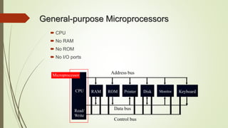
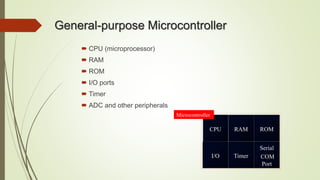
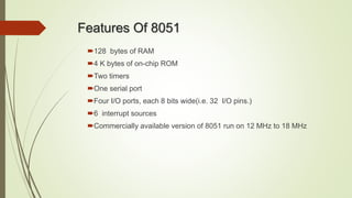
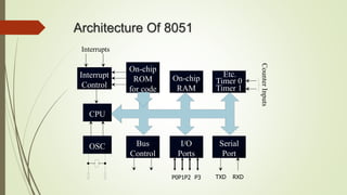
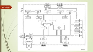
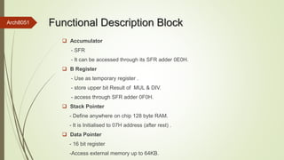
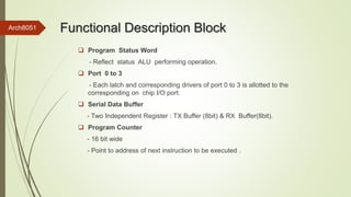
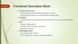
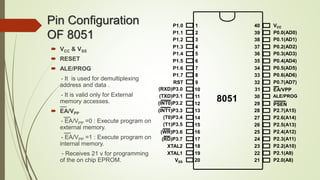
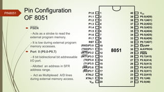
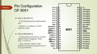
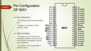

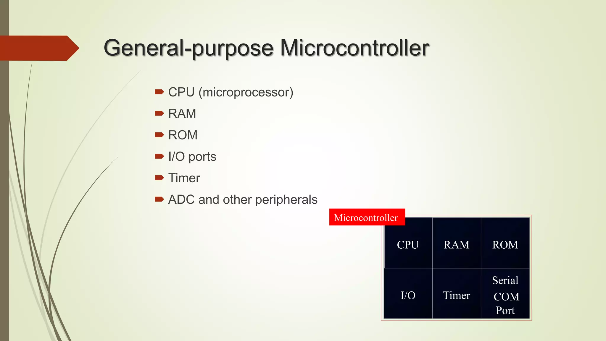
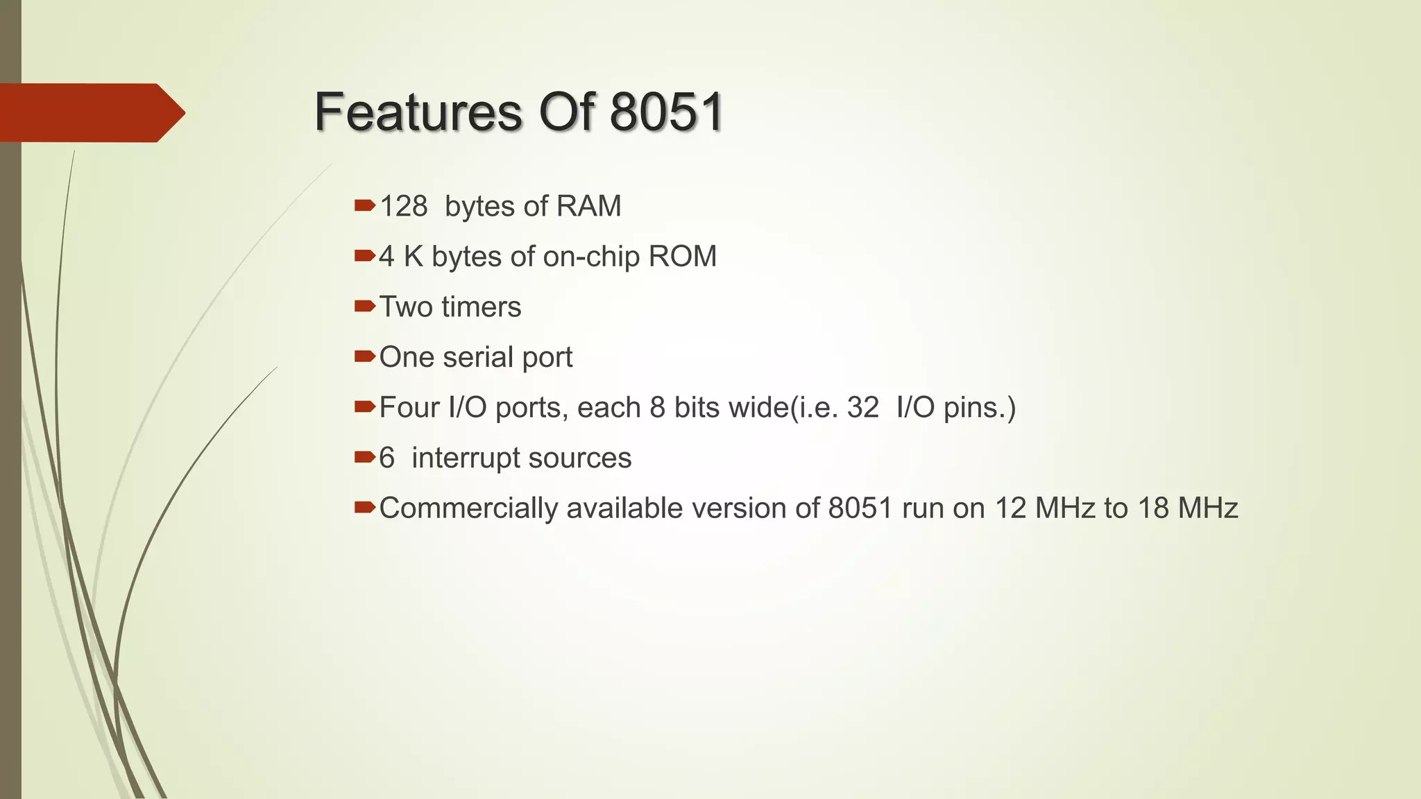
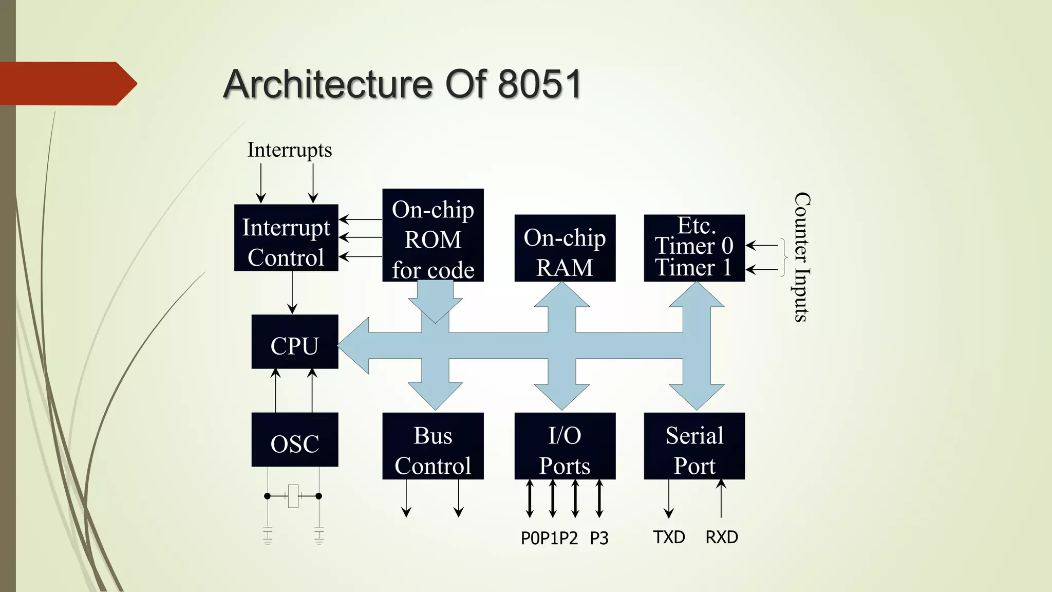
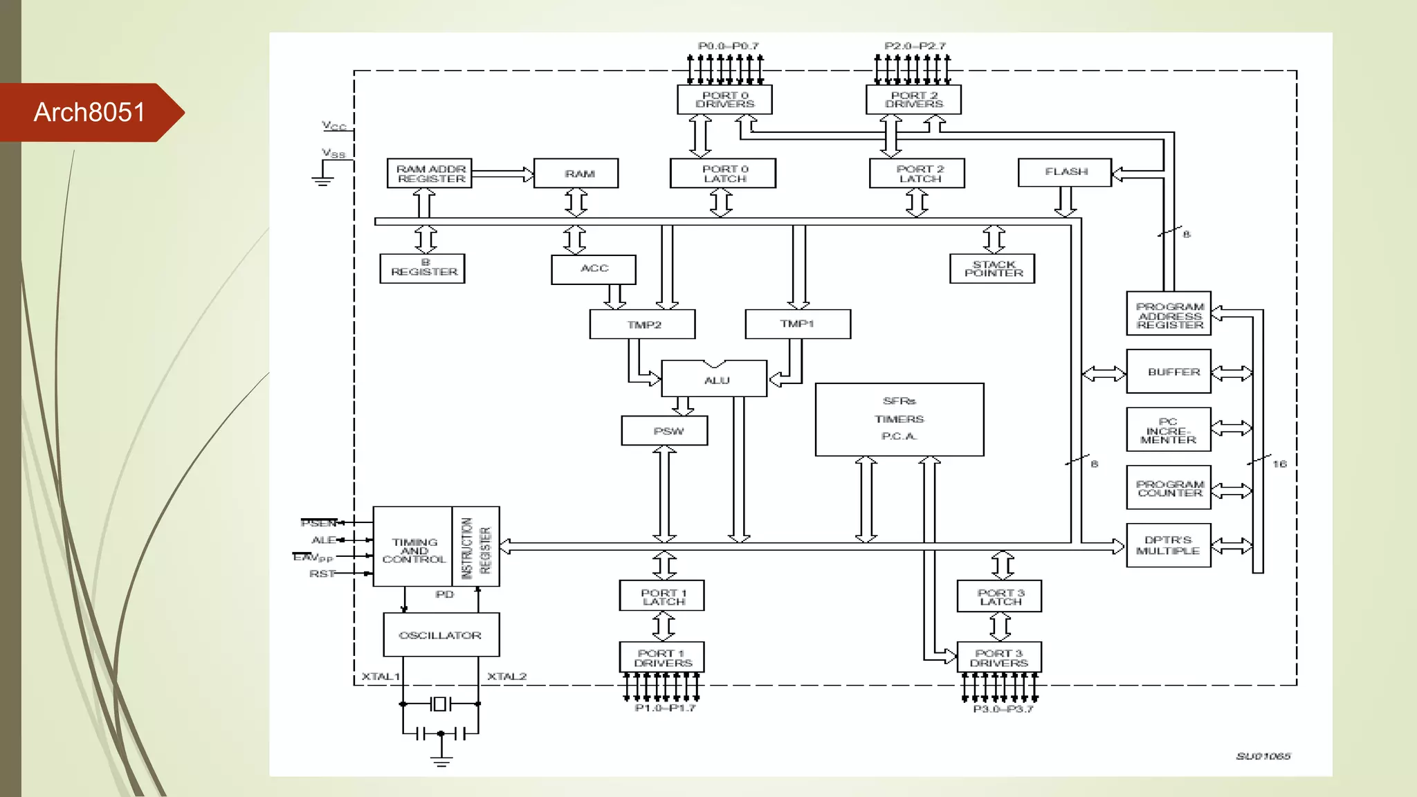
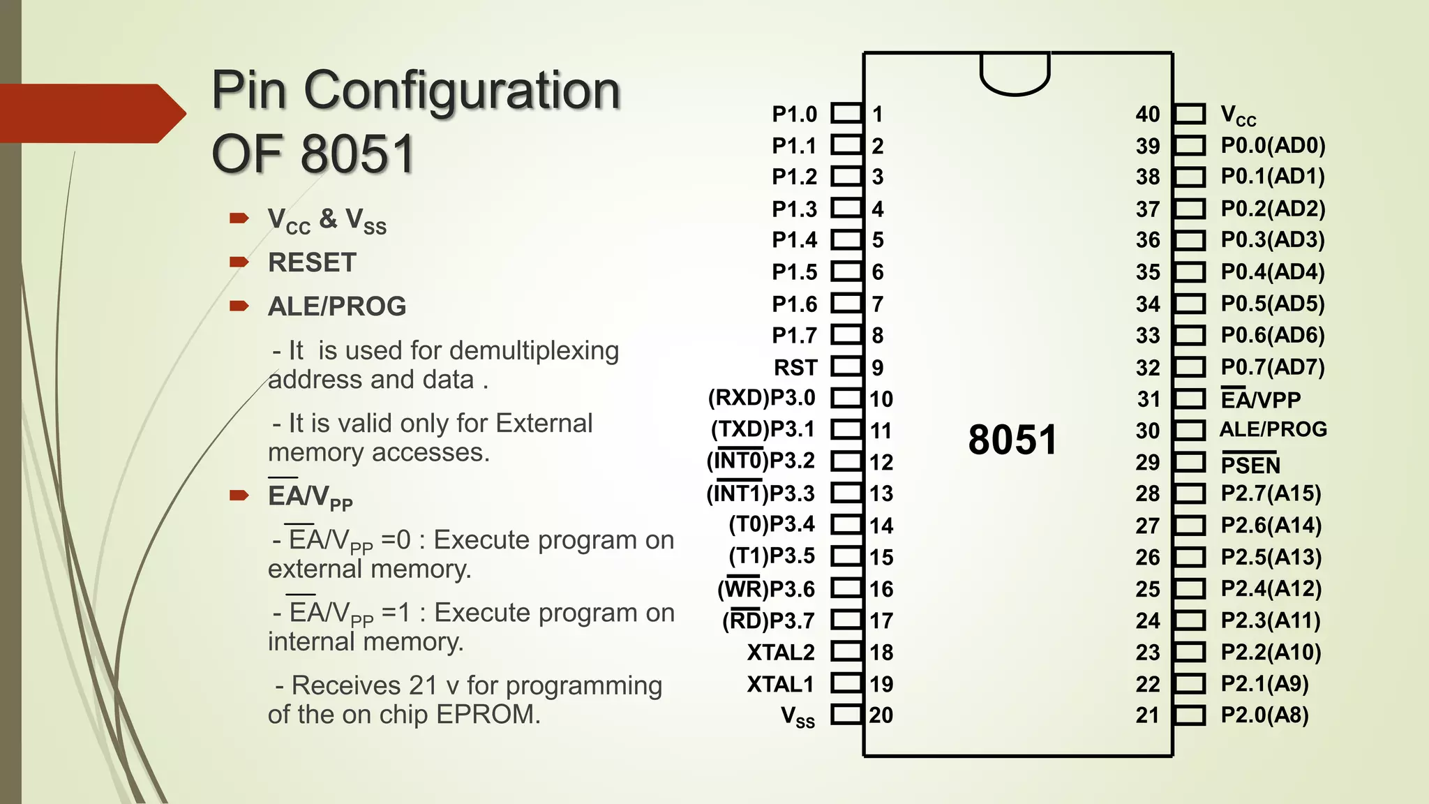
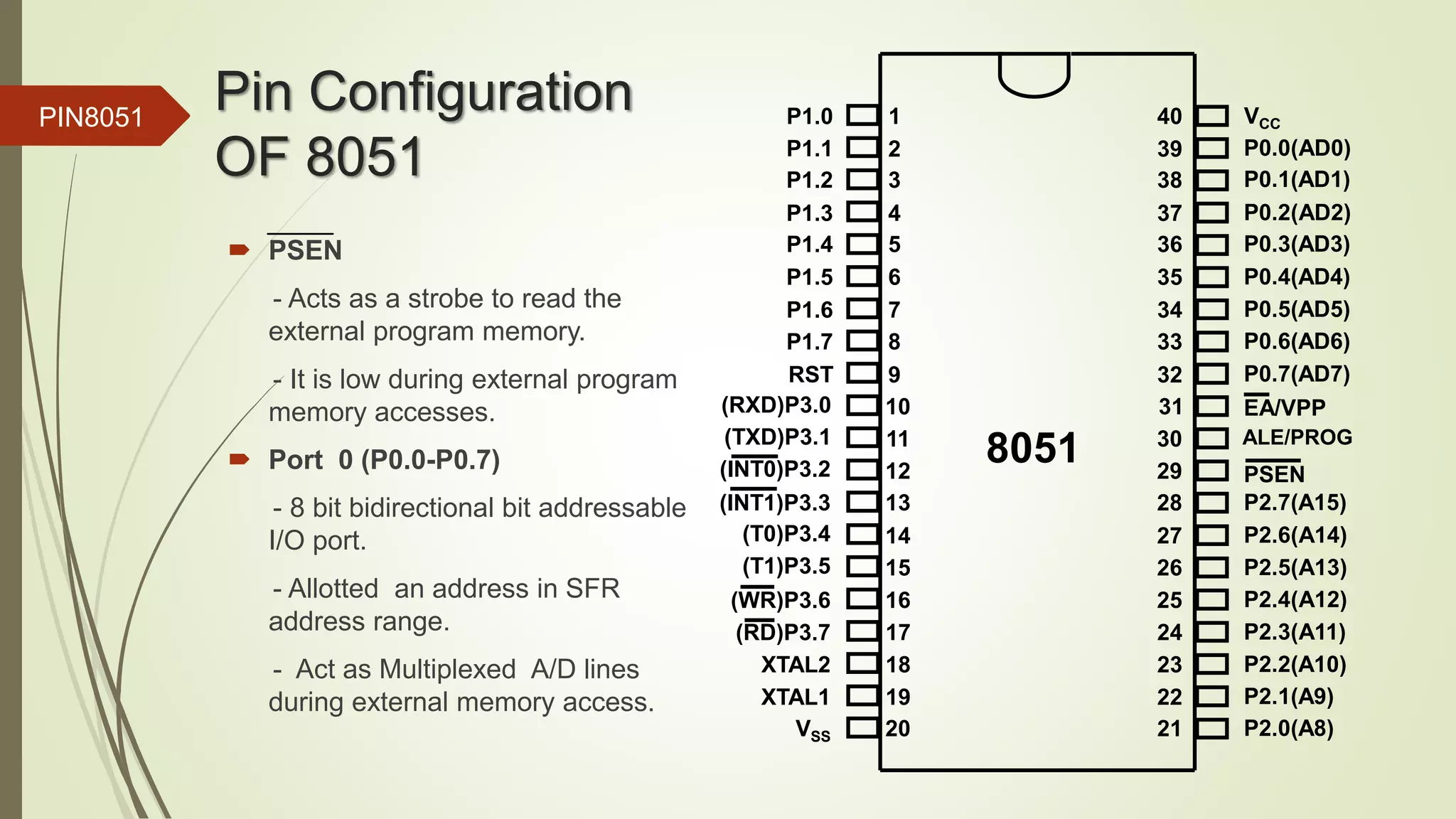
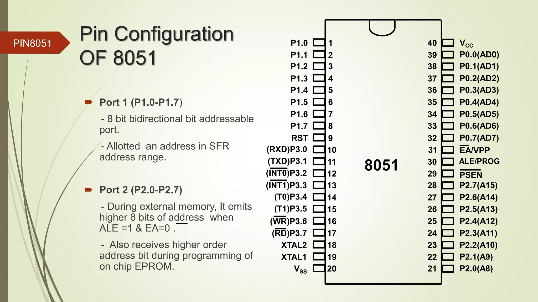
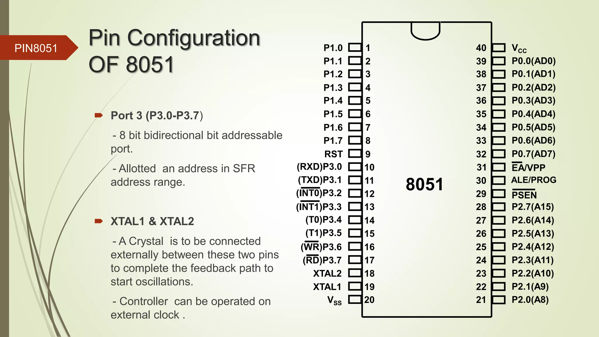


The document provides a detailed overview of the 8051 microcontroller architecture, including its features, pin configuration, and key functional components. It outlines specifications such as 128 bytes of RAM, 4KB of ROM, serial communication, multiple I/O ports, and various control signals. Additionally, it describes the roles of internal registers, timers, and the addressing scheme used within the microcontroller.


