Overview
Instruction SetProcessor (ISP)
Central Processing Unit (CPU)
A typical computing task consists of a series
of steps specified by a sequence of machine
instructions that constitute a program.
An instruction is executed by carrying out a
sequence of more rudimentary operations.
Fundamental Concepts
Processorfetches one instruction at a time and
perform the operation specified.
Instructions are fetched from successive memory
locations until a branch or a jump instruction is
encountered.
Processor keeps track of the address of the memory
location containing the next instruction to be fetched
using Program Counter (PC).
Instruction Register (IR)
5.
Executing an Instruction
Fetch the contents of the memory location pointed
to by the PC. The contents of this location are
loaded into the IR (fetch phase).
IR ← [[PC]]
Assuming that the memory is byte addressable,
increment the contents of the PC by 4 (fetch phase).
PC ← [PC] + 4
Carry out the actions specified by the instruction in
the IR (execution phase).
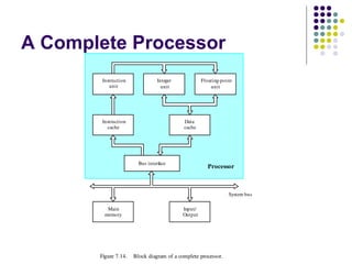
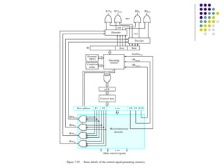
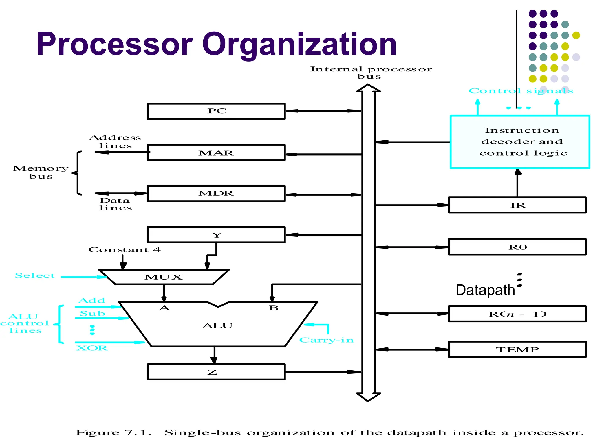
Internal organization ofthe
processor
ALU
Registers for temporary storage
Various digital circuits for executing different micro
operations.(gates, MUX,decoders,counters).
Internal path for movement of data between ALU
and registers.
Driver circuits for transmitting signals to external
units.
Receiver circuits for incoming signals from external
units.
8.
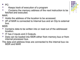
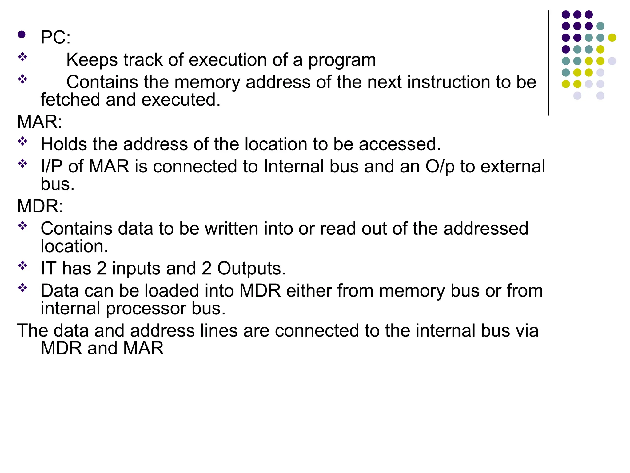
PC:
Keepstrack of execution of a program
Contains the memory address of the next instruction to be
fetched and executed.
MAR:
Holds the address of the location to be accessed.
I/P of MAR is connected to Internal bus and an O/p to external
bus.
MDR:
Contains data to be written into or read out of the addressed
location.
IT has 2 inputs and 2 Outputs.
Data can be loaded into MDR either from memory bus or from
internal processor bus.
The data and address lines are connected to the internal bus via
MDR and MAR
9.
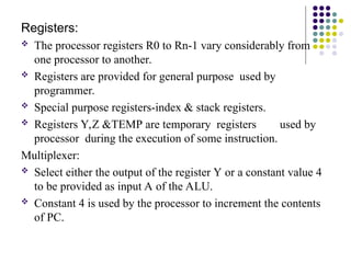
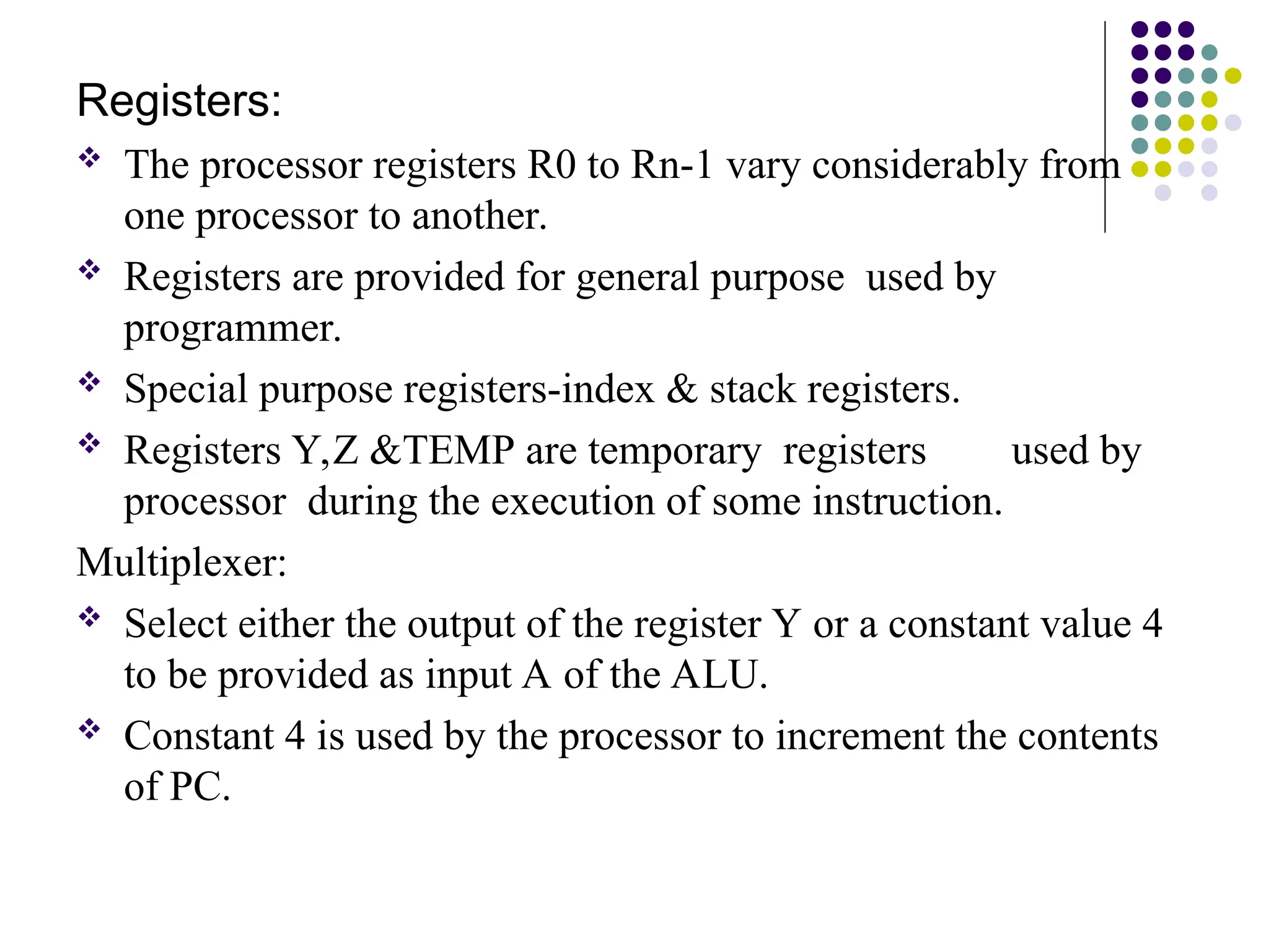
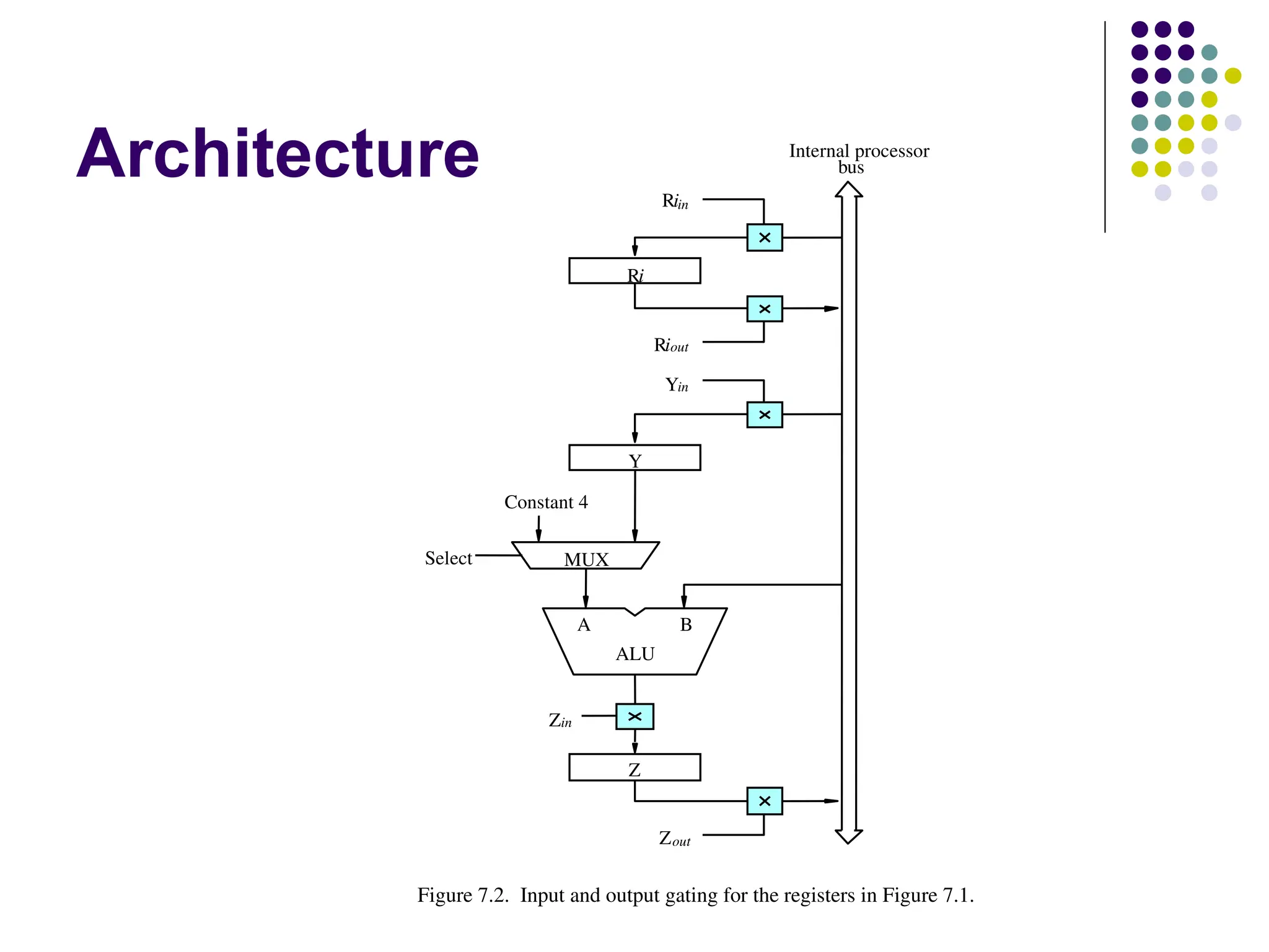
Registers:
The processorregisters R0 to Rn-1 vary considerably from
one processor to another.
Registers are provided for general purpose used by
programmer.
Special purpose registers-index & stack registers.
Registers Y,Z &TEMP are temporary registers used by
processor during the execution of some instruction.
Multiplexer:
Select either the output of the register Y or a constant value 4
to be provided as input A of the ALU.
Constant 4 is used by the processor to increment the contents
of PC.
10.
ALU:
Used to performarithmetic and logical
operation.
Data Path:
The registers, ALU and interconnecting bus are
collectively referred to as the data path.
11.
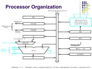
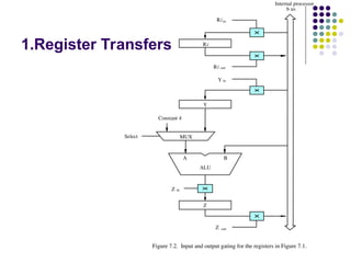
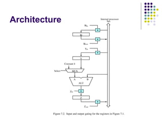
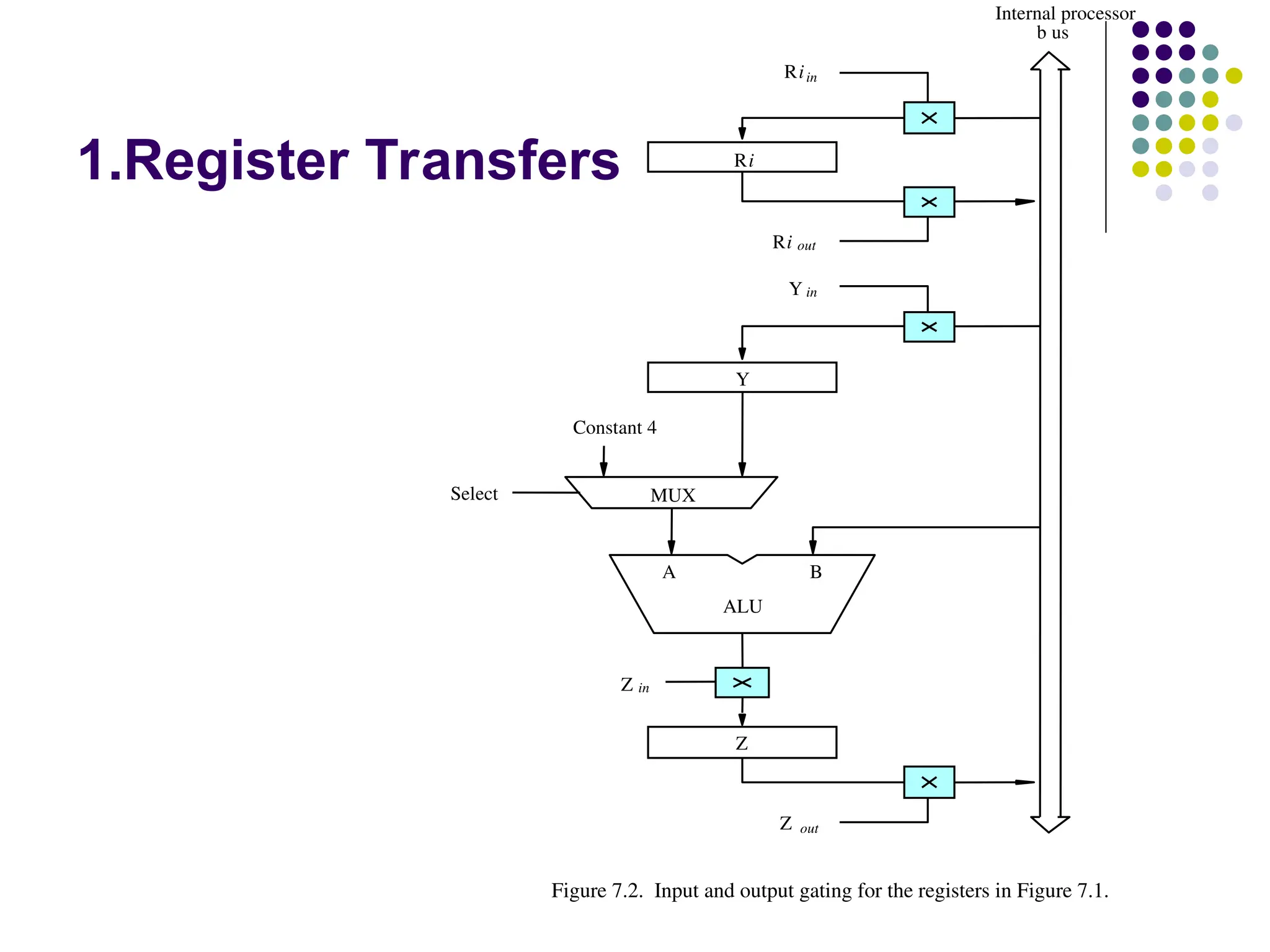
1.Register Transfers
B
A
Z
ALU
Y in
Y
Zin
Z out
Riin
Ri
Ri out
b us
Internal processor
Constant 4
MUX
Figure 7.2. Input and output gating for the registers in Figure 7.1.
Select
12.
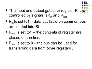
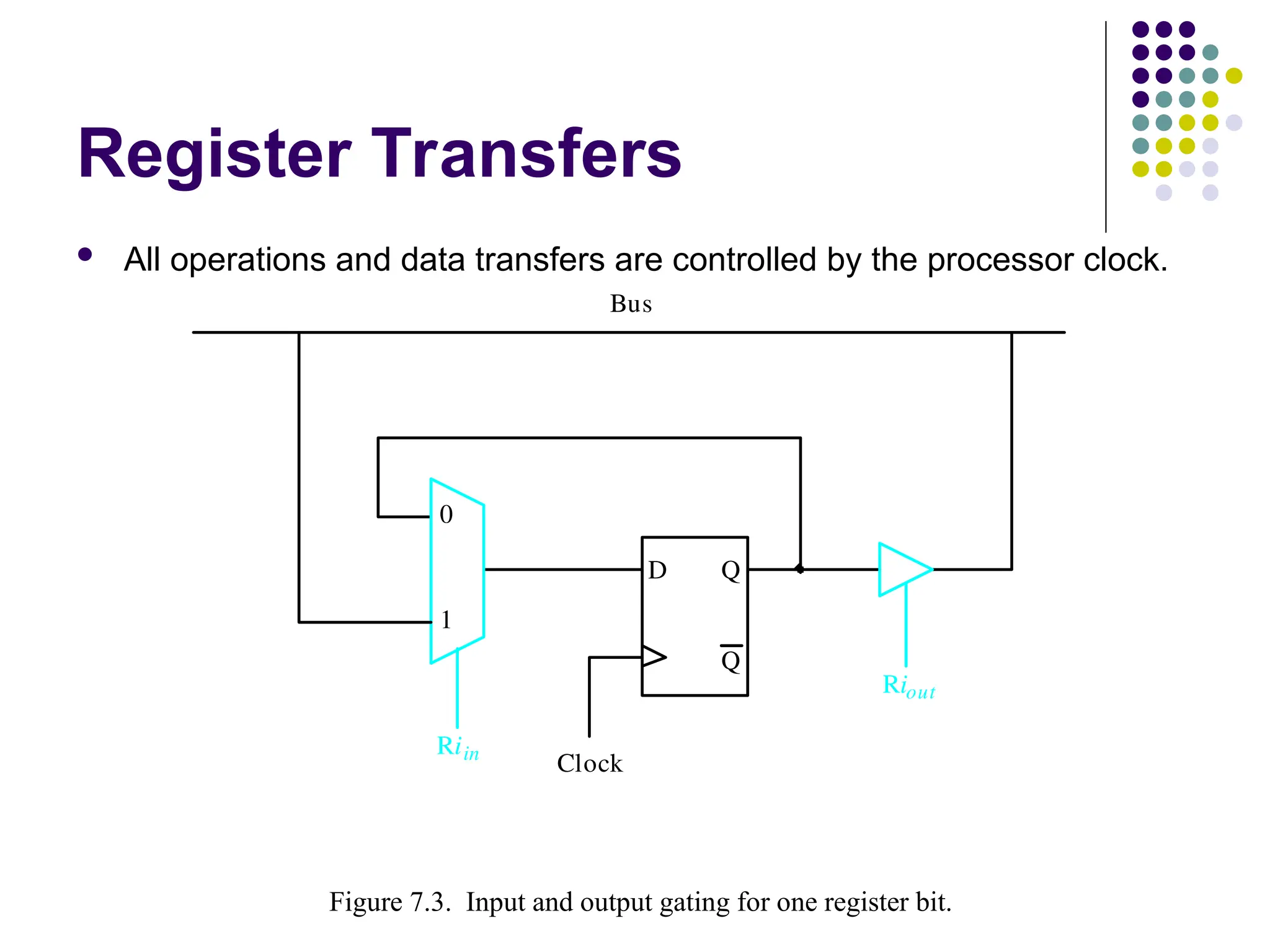
The inputand output gates for register Ri are
controlled by signals isRin and Riout .
Rin Is set to1 – data available on common bus
are loaded into Ri.
Riout Is set to1 – the contents of register are
placed on the bus.
Riout Is set to 0 – the bus can be used for
transferring data from other registers .
13.
Data transfer betweentwo
registers:
EX:
Transfer the contents of R1 to R4.
1. Enable output of register R1 by setting
R1out=1. This places the contents of R1 on
the processor bus.
2. Enable input of register R4 by setting
R4in=1. This loads the data from the
processor bus into register R4.
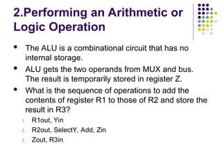
2.Performing an Arithmeticor
Logic Operation
The ALU is a combinational circuit that has no
internal storage.
ALU gets the two operands from MUX and bus.
The result is temporarily stored in register Z.
What is the sequence of operations to add the
contents of register R1 to those of R2 and store the
result in R3?
1. R1out, Yin
2. R2out, SelectY, Add, Zin
3. Zout, R3in
16.
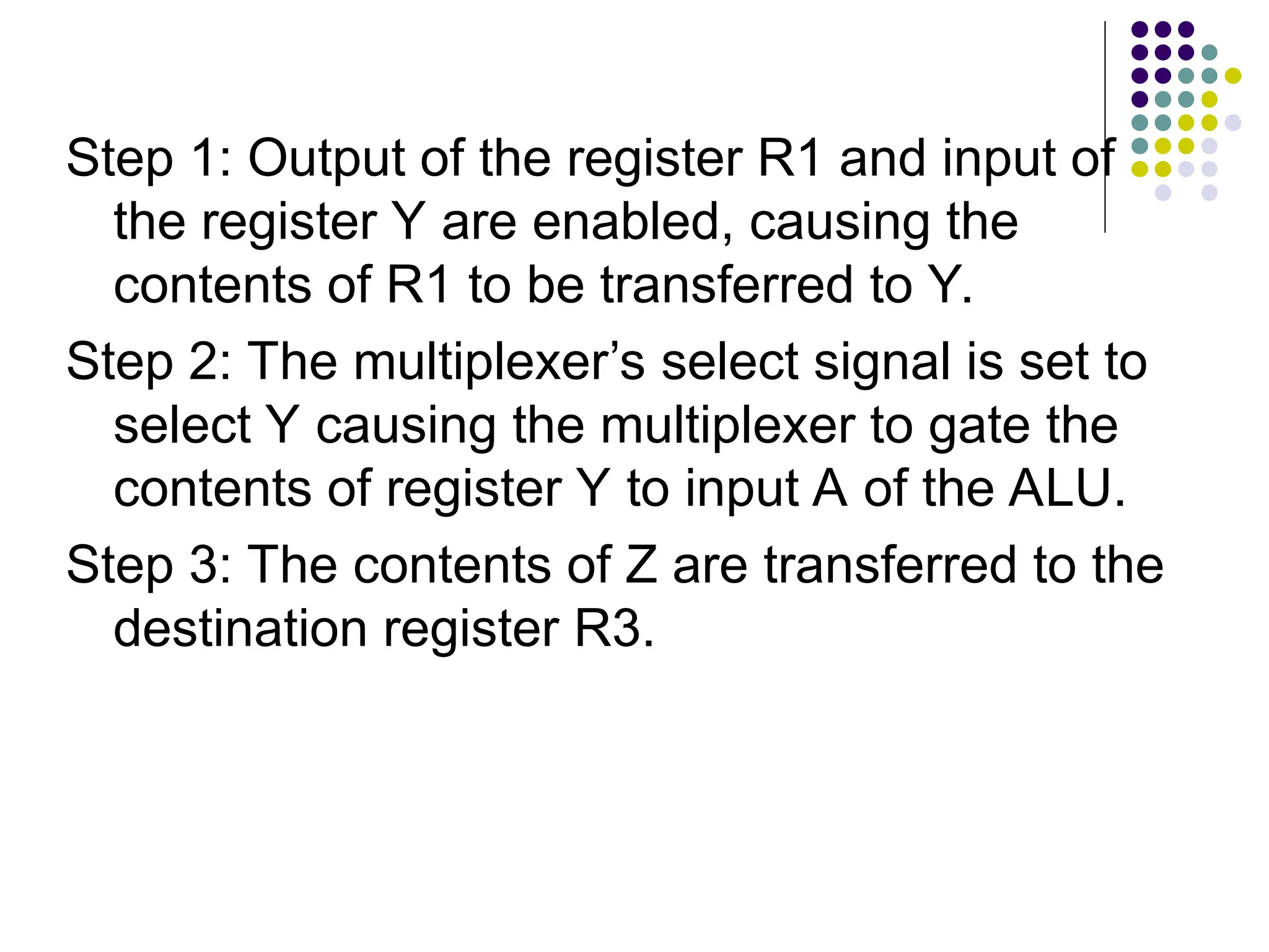
Step 1: Outputof the register R1 and input of
the register Y are enabled, causing the
contents of R1 to be transferred to Y.
Step 2: The multiplexer’s select signal is set to
select Y causing the multiplexer to gate the
contents of register Y to input A of the ALU.
Step 3: The contents of Z are transferred to the
destination register R3.
17.
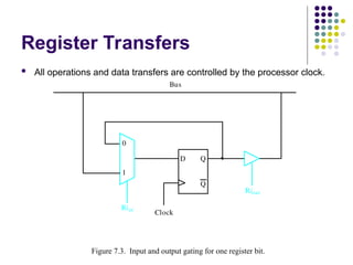
Register Transfers
Alloperations and data transfers are controlled by the processor clock.
Figure 7.3. Input and output gating for one register bit.
D Q
Q
Clock
1
0
Riout
Riin
Bus
Figure 7.3. Input and output gating for one register bit.
18.
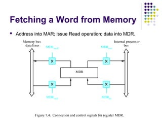
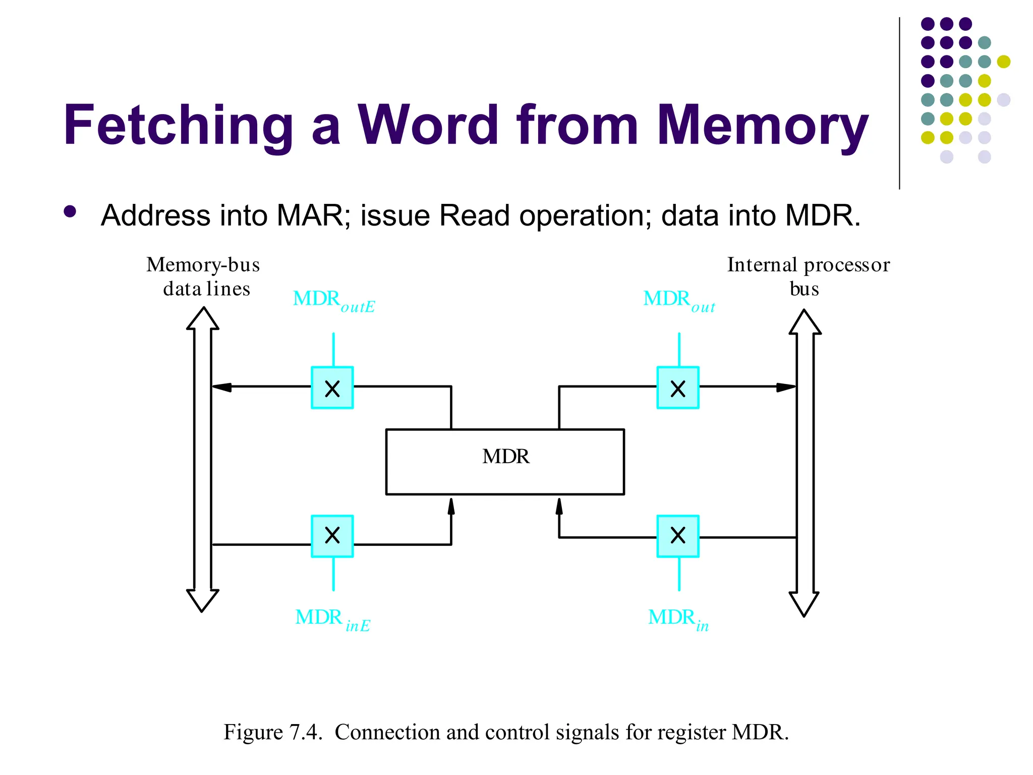
Fetching a Wordfrom Memory
Address into MAR; issue Read operation; data into MDR.
MDR
Memory-bus
Figure 7.4. Connection and control signals for register MDR.
data lines
Internal processor
bus
MDRout
MDRoutE
MDRin
MDRinE
Figure 7.4. Connection and control signals for register MDR.
19.
3.Fetching a Wordfrom
Memory
The response time of each memory access varies
(cache miss, memory-mapped I/O,…).
To accommodate this, the processor waits until it
receives an indication that the requested operation
has been completed (Memory-Function-Completed,
MFC).
Move (R1), R2
MAR ← [R1]
Start a Read operation on the memory bus
Wait for the MFC response from the memory
Load MDR from the memory bus
R2 ← [MDR]
20.
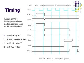
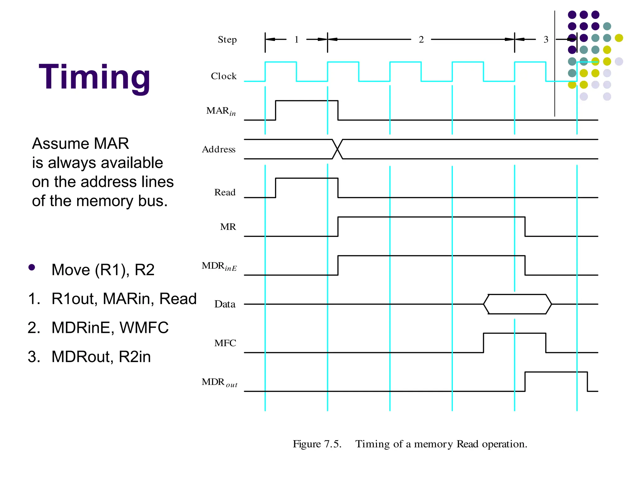
Timing
Figure 7.5. Timingof a memory Read operation.
1 2
Clock
Address
MR
Data
MFC
Read
MDRinE
MDRout
Step 3
MARin
Assume MAR
is always available
on the address lines
of the memory bus.
Move (R1), R2
1. R1out, MARin, Read
2. MDRinE, WMFC
3. MDRout, R2in
21.
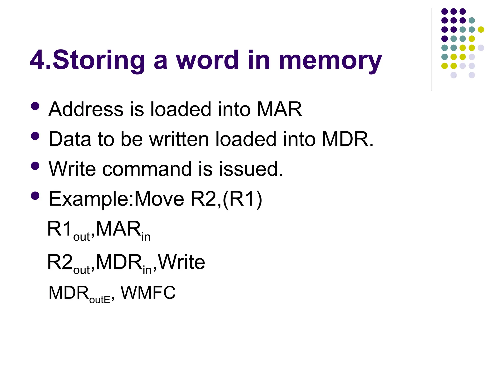
4.Storing a wordin memory
Address is loaded into MAR
Data to be written loaded into MDR.
Write command is issued.
Example:Move R2,(R1)
R1out,MARin
R2out,MDRin,Write
MDRoutE, WMFC
22.
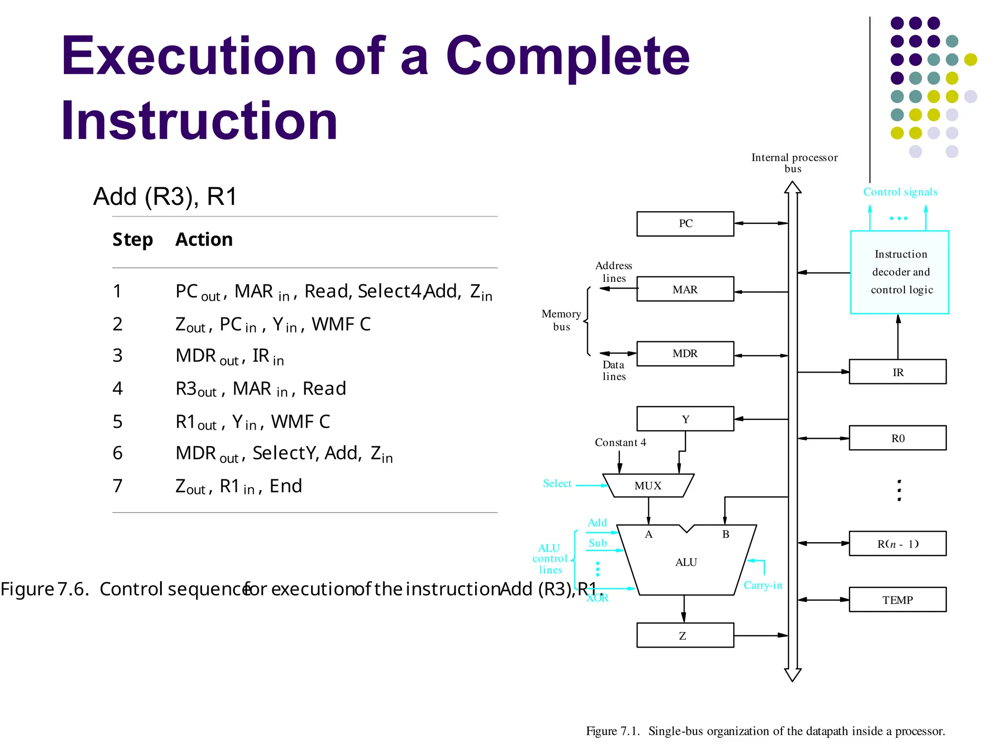
Execution of aComplete
Instruction
Add (R3), R1
Fetch the instruction
Fetch the first operand (the contents of the
memory location pointed to by R3)
Perform the addition
Load the result into R1
23.
Execution of aComplete
Instruction
Step Action
1 PC out , MAR in , Read, Select4,Add, Zin
2 Zout , PC in , Yin , WMF C
3 MDR out , IR in
4 R3out , MAR in , Read
5 R1out , Yin , WMF C
6 MDR out , SelectY, Add, Zin
7 Zout , R1in , End
Figure7.6. Control sequence
for executionof theinstructionAdd (R3),R1.
lines
Data
Address
lines
bus
Memory
Carry-in
ALU
PC
MAR
MDR
Y
Z
Add
XOR
Sub
bus
IR
TEMP
R0
control
ALU
lines
Control signals
R n 1
-
Instruction
decoder and
Internal processor
control logic
A B
Figure 7.1. Single-bus organization of the datapath inside a processor.
MUX
Select
Constant 4
Add (R3), R1
24.
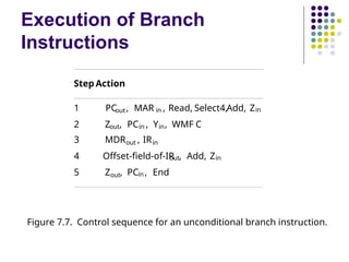
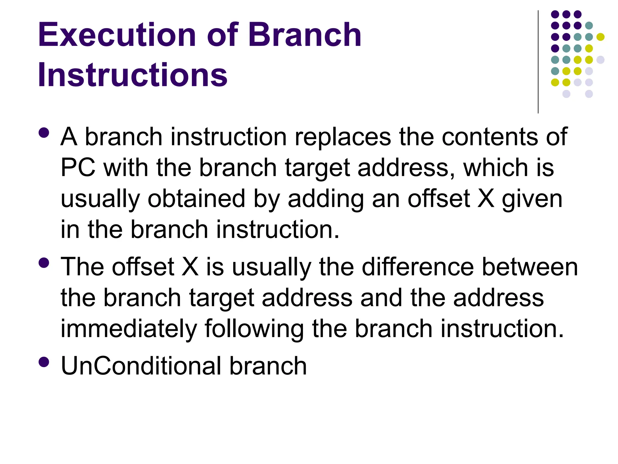
Execution of Branch
Instructions
A branch instruction replaces the contents of
PC with the branch target address, which is
usually obtained by adding an offset X given
in the branch instruction.
The offset X is usually the difference between
the branch target address and the address
immediately following the branch instruction.
UnConditional branch
25.
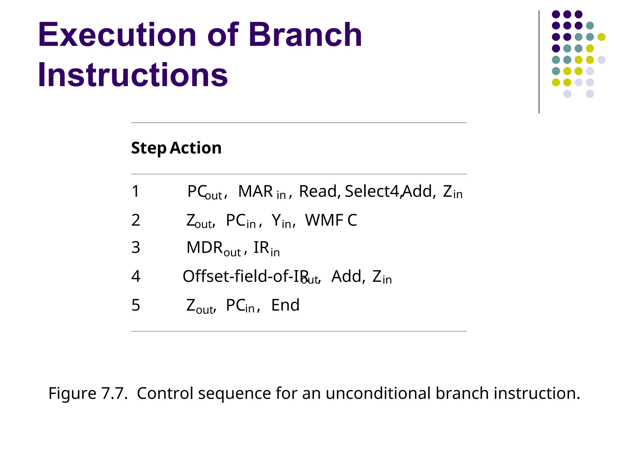
Execution of Branch
Instructions
StepAction
1 PCout, MAR in , Read, Select4,Add, Zin
2 Zout, PCin , Yin, WMF C
3 MDRout , IRin
4 Offset-field-of-IR
out, Add, Zin
5 Zout, PCin , End
Figure 7.7. Control sequence for an unconditional branch instruction.
26.
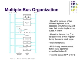
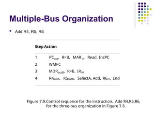
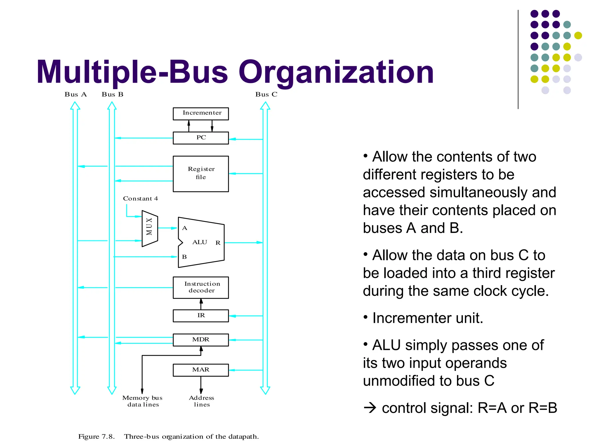
Multiple-Bus Organization
Memory bus
datalines
Figure 7.8. Three-bus organization of the datapath.
Bus A Bus B Bus C
Instruction
decoder
PC
Register
file
Constant 4
ALU
MDR
A
B
R
M
U
X
Incrementer
Address
lines
MAR
IR
• Allow the contents of two
different registers to be
accessed simultaneously and
have their contents placed on
buses A and B.
• Allow the data on bus C to
be loaded into a third register
during the same clock cycle.
• Incrementer unit.
• ALU simply passes one of
its two input operands
unmodified to bus C
control signal: R=A or R=B
27.
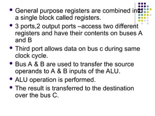
General purposeregisters are combined into
a single block called registers.
3 ports,2 output ports –access two different
registers and have their contents on buses A
and B
Third port allows data on bus c during same
clock cycle.
Bus A & B are used to transfer the source
operands to A & B inputs of the ALU.
ALU operation is performed.
The result is transferred to the destination
over the bus C.
28.
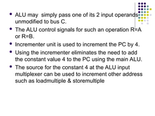
ALU maysimply pass one of its 2 input operands
unmodified to bus C.
The ALU control signals for such an operation R=A
or R=B.
Incrementer unit is used to increment the PC by 4.
Using the incrementer eliminates the need to add
the constant value 4 to the PC using the main ALU.
The source for the constant 4 at the ALU input
multiplexer can be used to increment other address
such as loadmultiple & storemultiple
29.
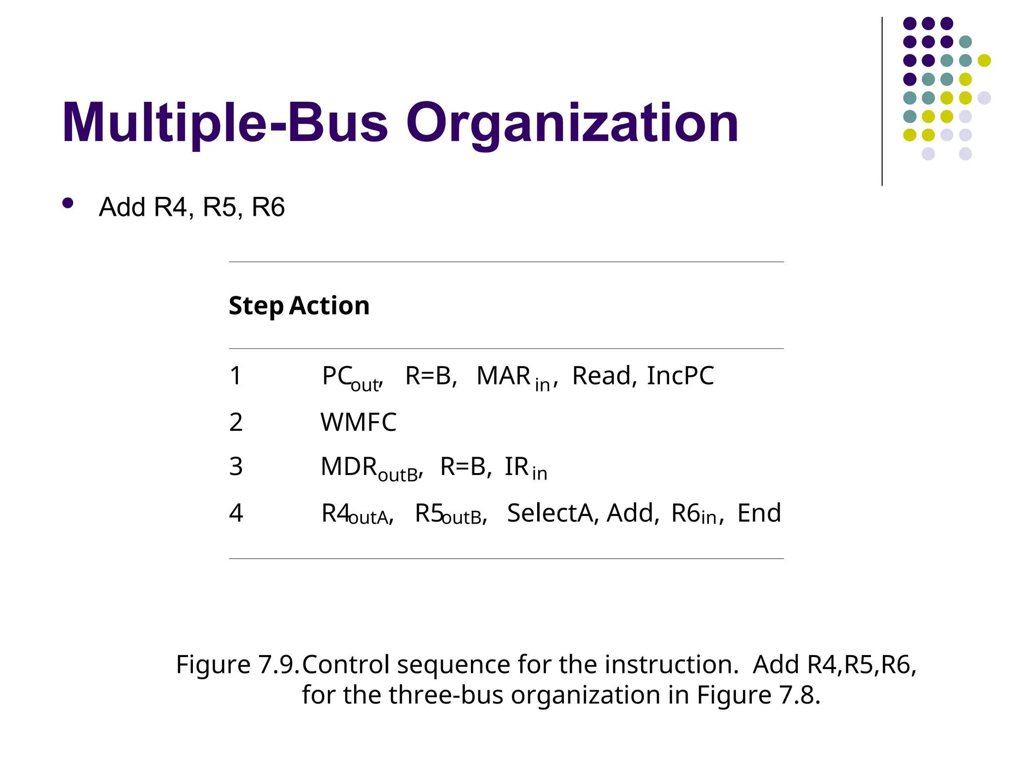
Multiple-Bus Organization
AddR4, R5, R6
Step Action
1 PCout, R=B, MAR in, Read, IncPC
2 WMFC
3 MDRoutB, R=B, IRin
4 R4outA, R5outB, SelectA, Add, R6in, End
Figure 7.9.Control sequence for the instruction. Add R4,R5,R6,
for the three-bus organization in Figure 7.8.
30.
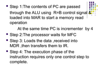
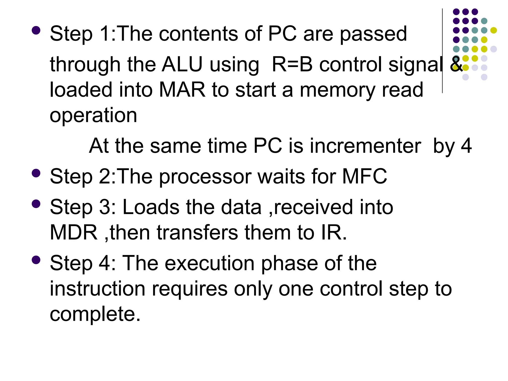
Step 1:Thecontents of PC are passed
through the ALU using R=B control signal &
loaded into MAR to start a memory read
operation
At the same time PC is incrementer by 4
Step 2:The processor waits for MFC
Step 3: Loads the data ,received into
MDR ,then transfers them to IR.
Step 4: The execution phase of the
instruction requires only one control step to
complete.
31.
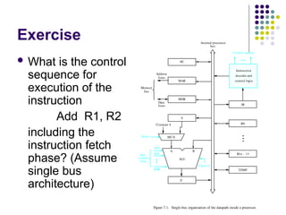
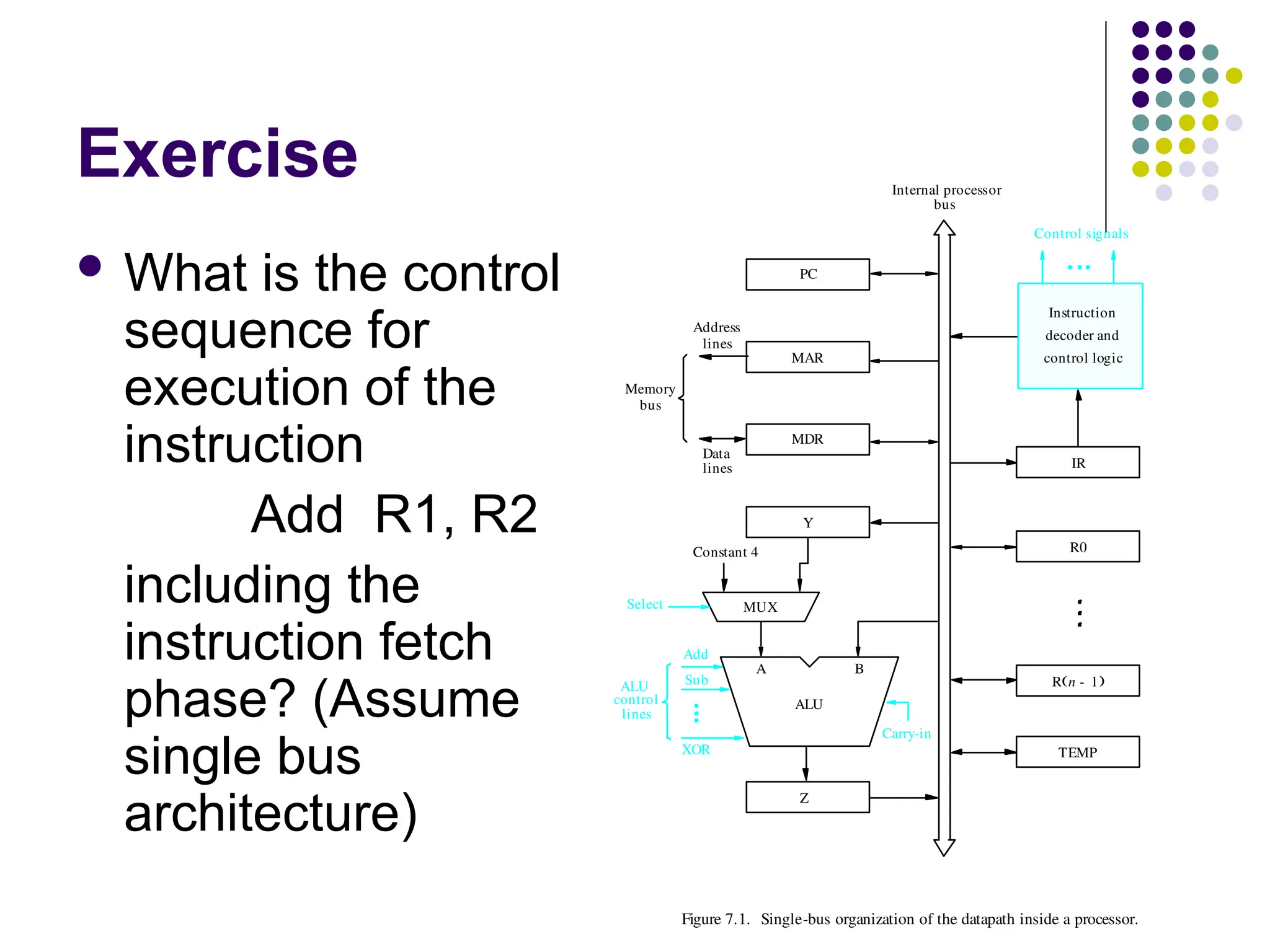
Exercise
What isthe control
sequence for
execution of the
instruction
Add R1, R2
including the
instruction fetch
phase? (Assume
single bus
architecture)
lines
Data
Address
lines
bus
Memory
Carry-in
ALU
PC
MAR
MDR
Y
Z
Add
XOR
Sub
bus
IR
TEMP
R0
control
ALU
lines
Control signals
R n 1
-
Instruction
decoder and
Internal processor
control logic
A B
Figure 7.1. Single-bus organization of the datapath inside a processor.
MUX
Select
Constant 4
Overview
To executeinstructions, the processor must
have some means of generating the control
signals needed in the proper sequence.
Two categories: hardwired control and
microprogrammed control
Hardwired system can operate at high speed;
but with little flexibility.
34.
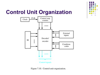
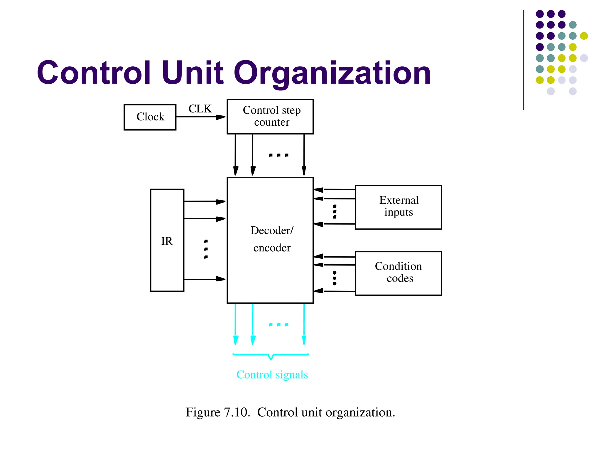
Control Unit Organization
Figure7.10. Control unit organization.
CLK
Clock
Control step
IR
encoder
Decoder/
Control signals
codes
counter
inputs
Condition
External
35.
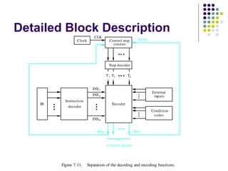
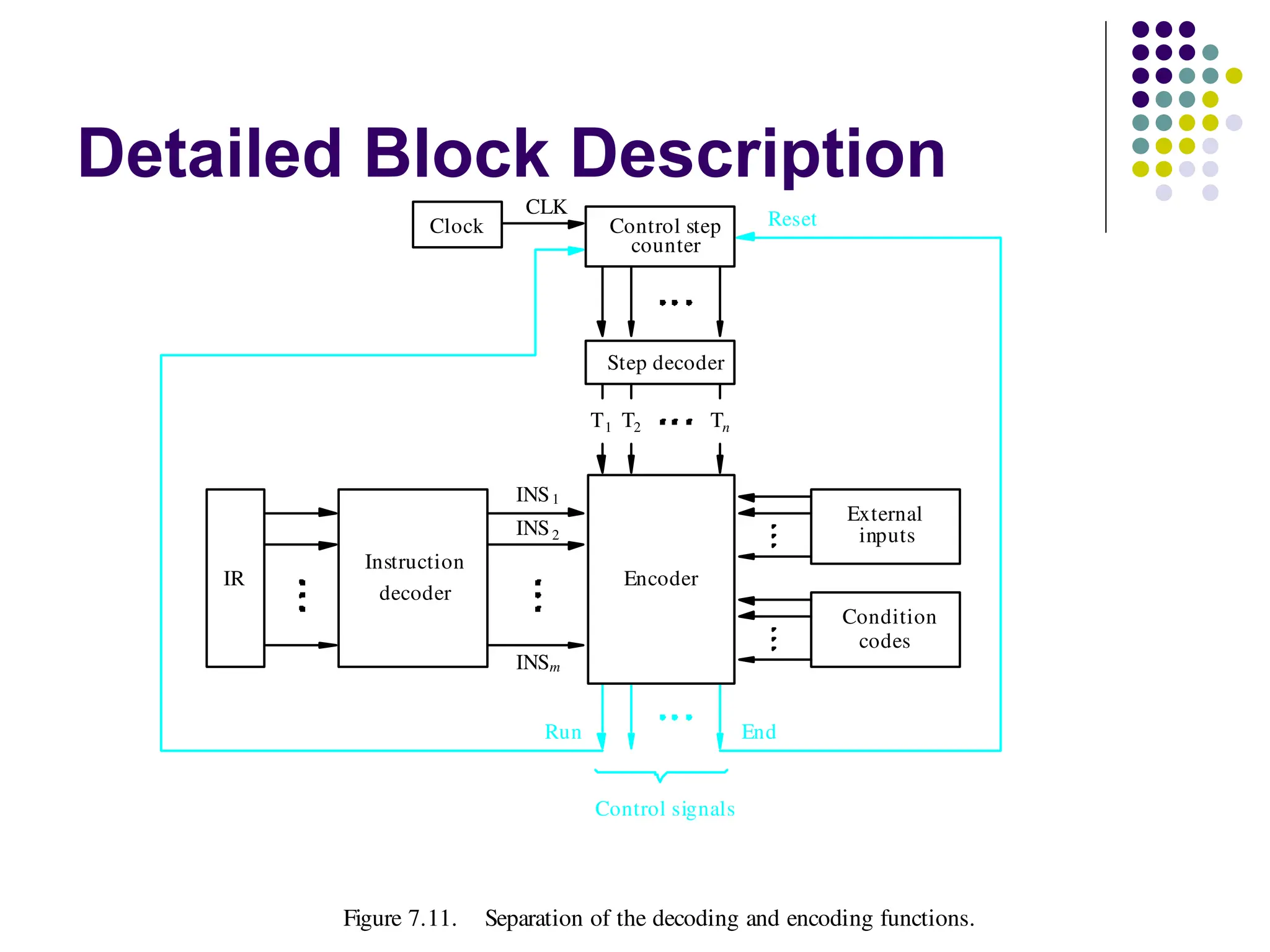
Detailed Block Description
External
inputs
Figure7.11. Separation of the decoding and encoding functions.
Encoder
Reset
CLK
Clock
Control signals
counter
Run End
Condition
codes
decoder
Instruction
Step decoder
Control step
IR
T1 T2 Tn
INS1
INS2
INSm
36.
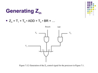
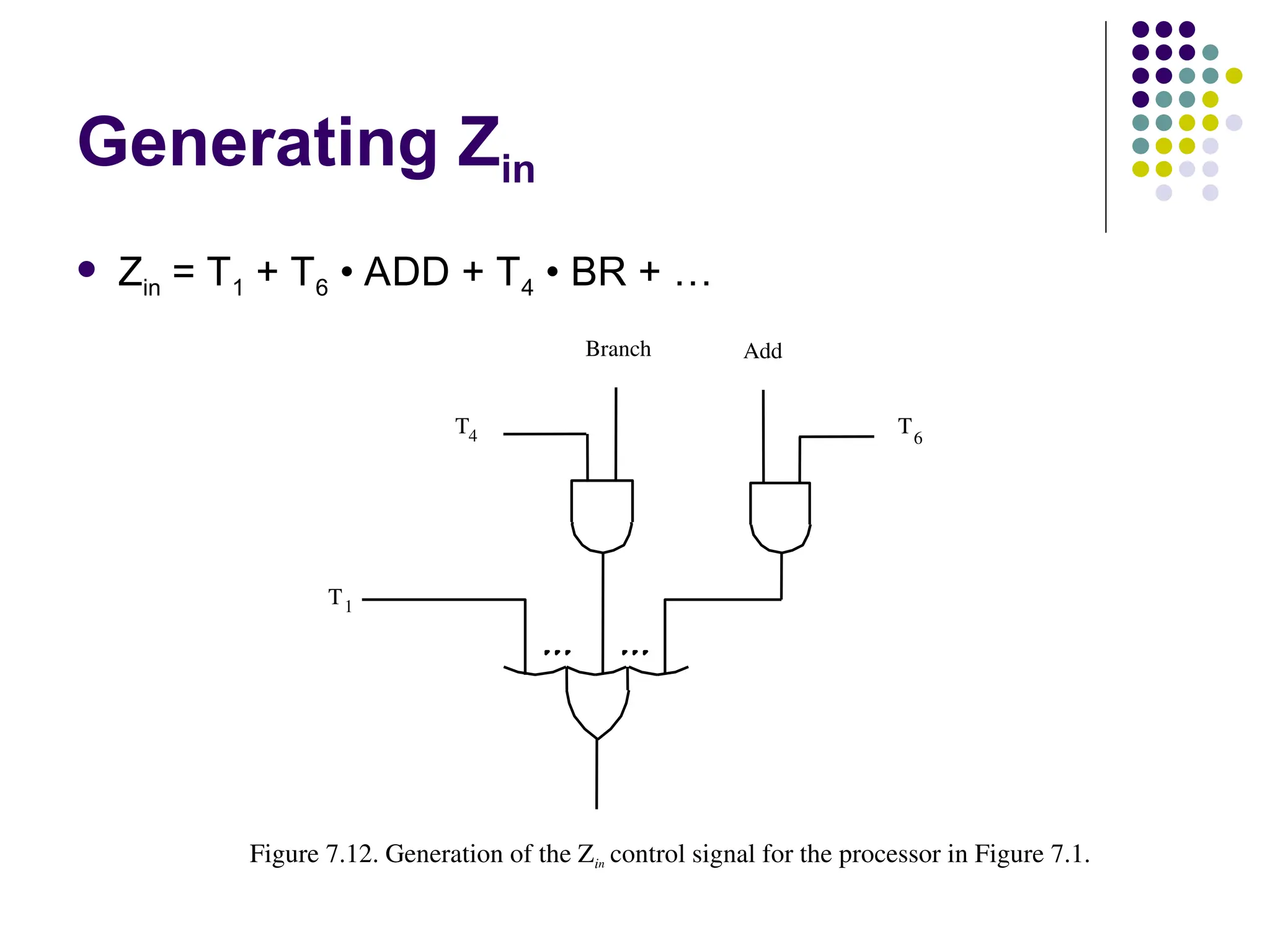
Generating Zin
Zin= T1 + T6 • ADD + T4 • BR + …
Figure 7.12. Generation of the Zin control signal for the processor in Figure 7.1.
T1
Add
Branch
T4 T6
37.
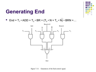
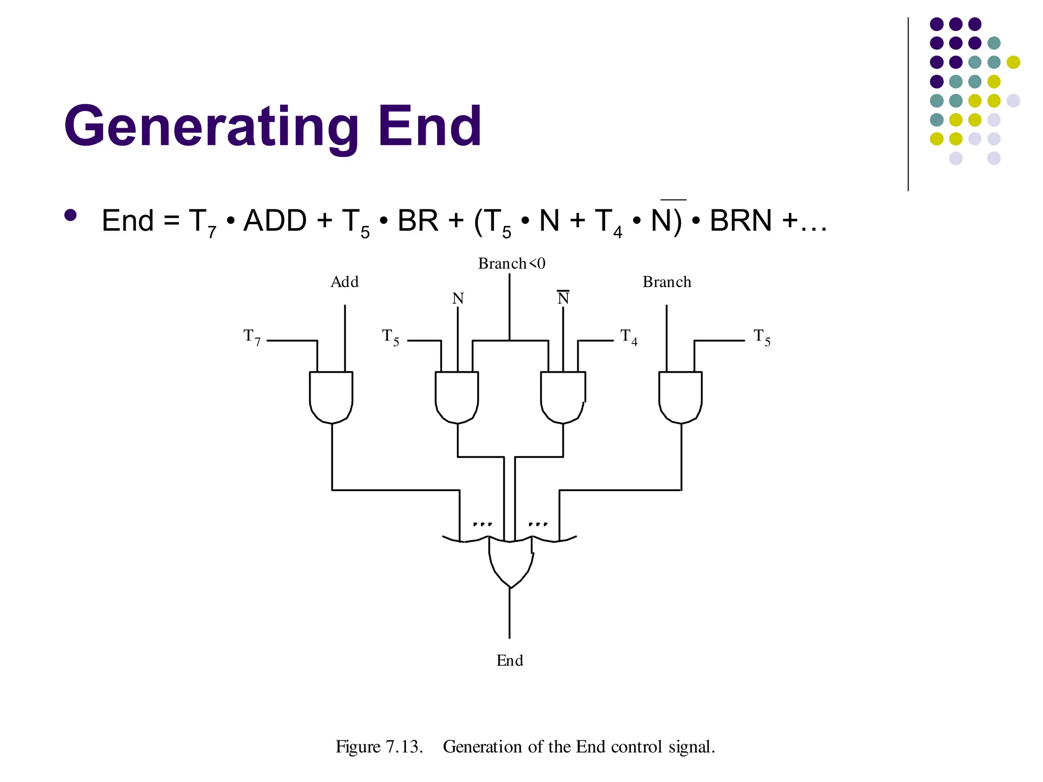
Generating End
End= T7 • ADD + T5 • BR + (T5 • N + T4 • N) • BRN +…
Figure 7.13. Generation of the End control signal.
T7
Add Branch
Branch<0
T5
End
N
N
T4
T5
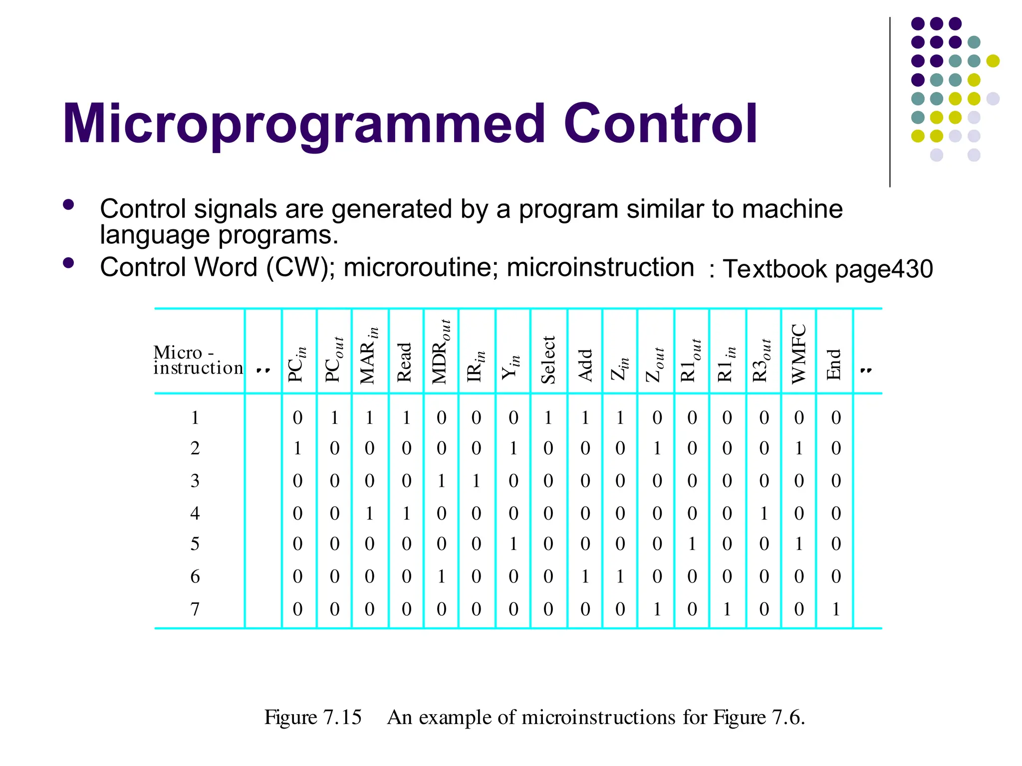
Microprogrammed Control
Controlsignals are generated by a program similar to machine
language programs.
Control Word (CW); microroutine; microinstruction
PC
in
PC
out
MAR
in
Read
MDR
out
IR
in
Y
in
Select
Add
Z
in
Z
out
R1
out
R1
in
R3
out
WMFC
End
0
1
0
0
0
0
0
0
0
0
0
0
0
1
1
0
0
0
0
0
0
1
0
0
1
0
0
0
1
0
0
1
0
0
0
0
0
1
0
0
1
0
0
0
1
0
0
0
0
0
1
0
0
1
0
0
1
0
0
0
0
0
0
1
0
0
0
0
1
0
1
0
0
0
0
1
0
0
1
0
0
0
0
1
0
0
0
0
1
0
0
0
0
0
0
0
0
1
0
0
0
1
0
0
0
0
1
0
0
1
0
0
Micro -
instruction
1
2
3
4
5
6
7
Figure 7.15 An example of microinstructions for Figure 7.6.
: Textbook page430
41.
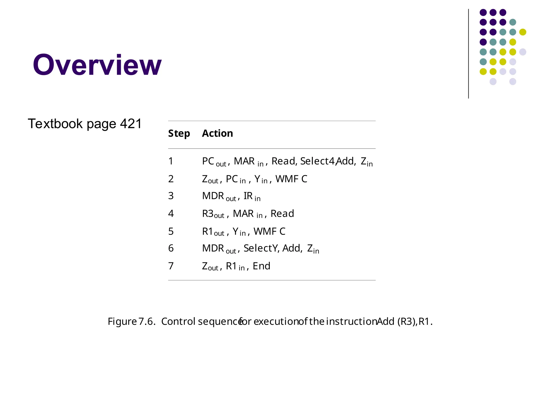
Overview
Step Action
1 PCout , MAR in , Read, Select4,Add, Zin
2 Zout , PC in , Yin , WMF C
3 MDR out , IR in
4 R3out , MAR in , Read
5 R1out , Yin , WMF C
6 MDR out , SelectY, Add, Zin
7 Zout , R1in , End
Figure7.6. Control sequence
for executionof theinstructionAdd (R3),R1.
Textbook page 421
42.
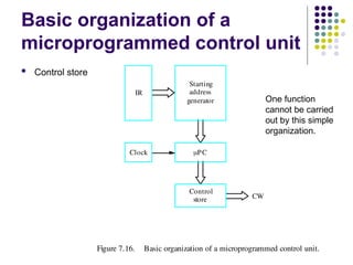
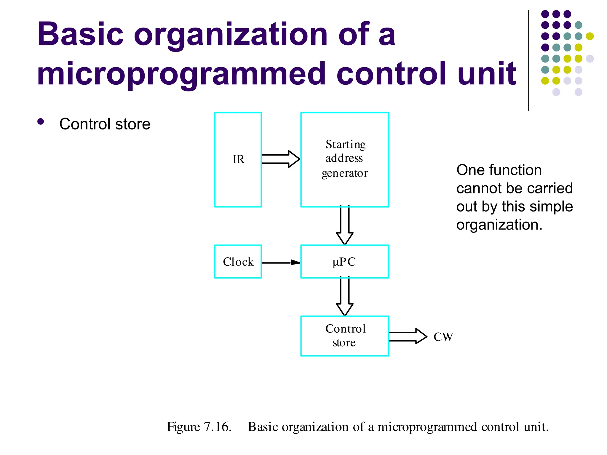
Basic organization ofa
microprogrammed control unit
Control store
Figure 7.16. Basic organization of a microprogrammed control unit.
store
Control
generator
Starting
address
CW
Clock PC
IR
One function
cannot be carried
out by this simple
organization.
43.
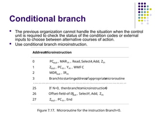
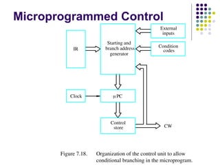
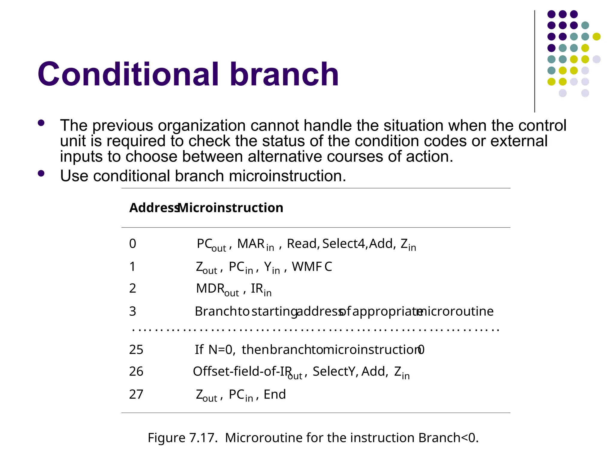
Conditional branch
Theprevious organization cannot handle the situation when the control
unit is required to check the status of the condition codes or external
inputs to choose between alternative courses of action.
Use conditional branch microinstruction.
Address
Microinstruction
0 PCout , MARin , Read,Select4,Add, Zin
1 Zout , PCin , Yin , WMF C
2 MDRout , IRin
3 Branchtostartingaddress
ofappropriate
microroutine
. ... .. ... ... .. ... .. ... ... .. ... ... .. ... .. ... ... .. ... .. ... ... .. ... ..
25 If N=0, thenbranchtomicroinstruction
0
26 Offset-field-of-IR
out , SelectY, Add, Zin
27 Zout , PCin , End
Figure 7.17. Microroutine for the instruction Branch<0.
44.
Microprogrammed Control
Figure 7.18.Organization of the control unit to allow
conditional branching in the microprogram.
Control
store
Clock
generator
Starting and
branch address Condition
codes
inputs
External
CW
IR
PC
45.
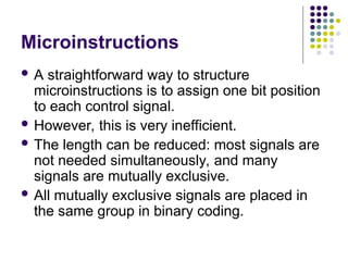
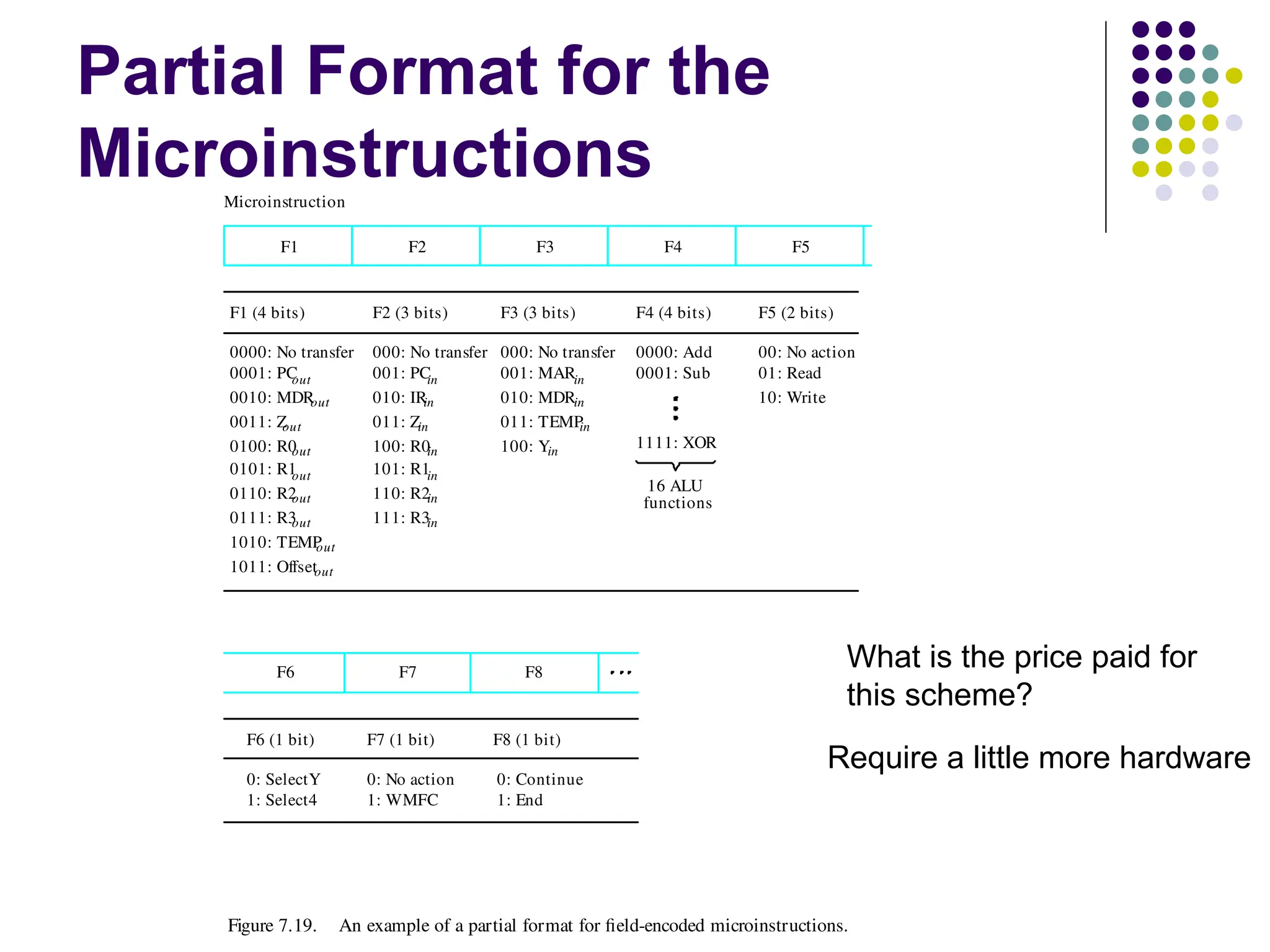
Microinstructions
A straightforwardway to structure
microinstructions is to assign one bit position
to each control signal.
However, this is very inefficient.
The length can be reduced: most signals are
not needed simultaneously, and many
signals are mutually exclusive.
All mutually exclusive signals are placed in
the same group in binary coding.
46.
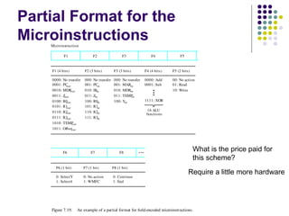
Partial Format forthe
Microinstructions
F2 (3 bits)
000: No transfer
001: PC
in
010: IR
in
011: Zin
100: R0in
101: R1in
110: R2in
111: R3in
F1 F2 F3 F4 F5
F1 (4 bits) F3 (3 bits) F4 (4 bits) F5 (2 bits)
0000: No transfer
0001: PC
out
0010: MDR
out
0011: Z
out
0100: R0
out
0101: R1
out
0110: R2
out
0111: R3
out
1010: TEMP
out
1011: Offsetout
000: No transfer
001: MARin
010: MDRin
011: TEMP
in
100: Yin
0000: Add
0001: Sub
1111: XOR
16 ALU
functions
00: No action
01: Read
10: Write
F6 F7 F8
F6 (1 bit) F7 (1 bit) F8 (1 bit)
0: SelectY
1: Select4
0: No action
1: WMFC
0: Continue
1: End
Figure 7.19. An example of a partial format for field-encoded microinstructions.
Microinstruction
What is the price paid for
this scheme?
Require a little more hardware
47.
Further Improvement
Enumeratethe patterns of required signals in
all possible microinstructions. Each
meaningful combination of active control
signals can then be assigned a distinct code.
Vertical organization
Horizontal organization
Textbook page 434
48.
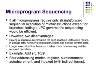
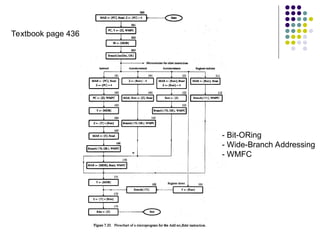
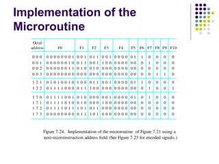
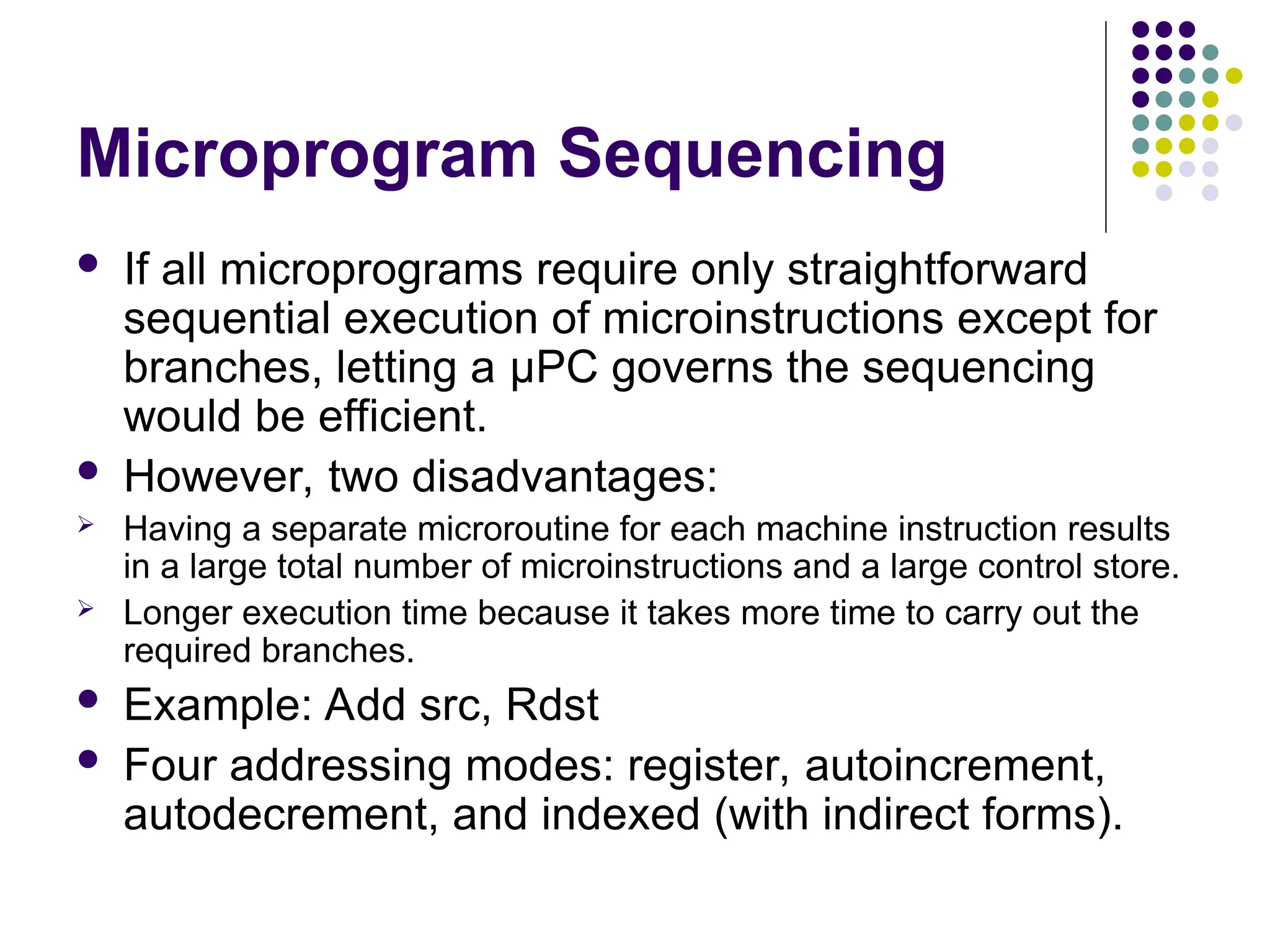
Microprogram Sequencing
Ifall microprograms require only straightforward
sequential execution of microinstructions except for
branches, letting a μPC governs the sequencing
would be efficient.
However, two disadvantages:
Having a separate microroutine for each machine instruction results
in a large total number of microinstructions and a large control store.
Longer execution time because it takes more time to carry out the
required branches.
Example: Add src, Rdst
Four addressing modes: register, autoincrement,
autodecrement, and indexed (with indirect forms).
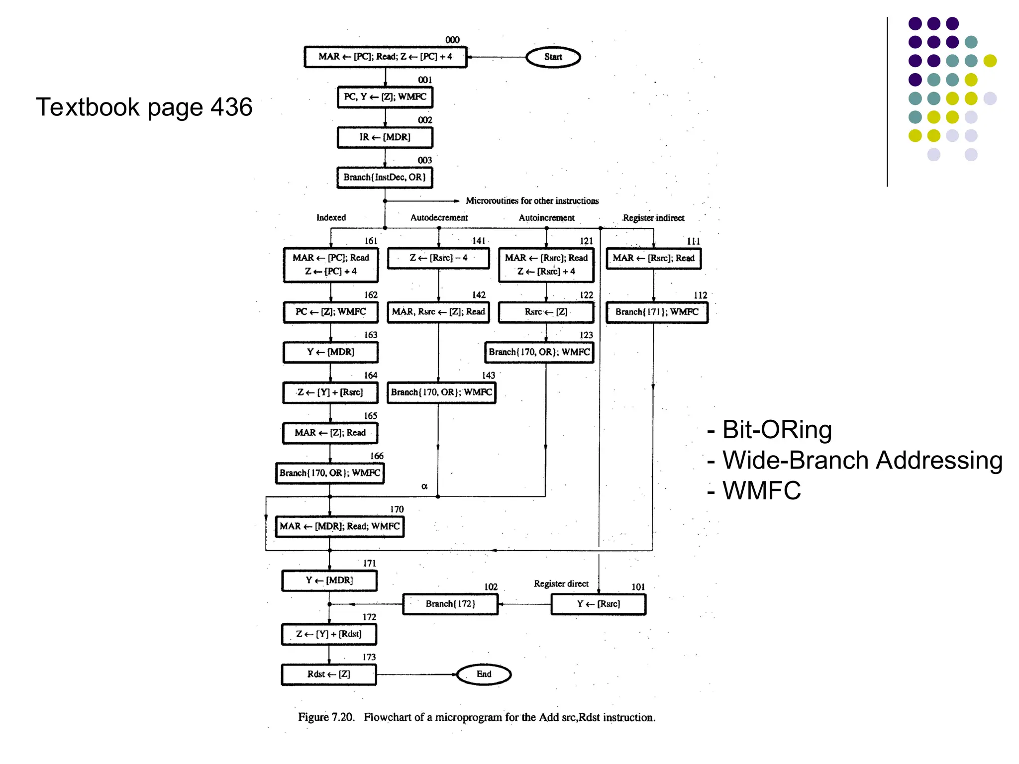
OP code 01 0 Rsrc Rdst
Mode
Contents of IR
0
3
4
7
8
10
11
Figure 7.21. Microinstruction for Add (Rsrc)+,Rdst.
Note: Microinstruction at location 170 is not executed for this addressing mode.
Address Microinstruction
(octal)
000 PCout, MARin , Read, Select
4 , Add, Zin
001 Zout, PCin, Yin, WMFC
002 MDRout, IRin
003 Branch {
PC 101 (from Instruction decoder);
PC5,4 [IR10,9]; PC3
121 Rsrcout, MARin , Read, Select4, Add, Z
in
122 Zout , Rsrcin
123
170 MDRout, MARin , Read, WMFC
171 MDRout, Yin
172 Rdstout , SelectY
, Add, Zin
173 Zout , Rdstin, End
[IR10][IR9][IR8]}
Branch {PC 170;PC0 [IR8]}, WMFC
Textbook page 439
51.
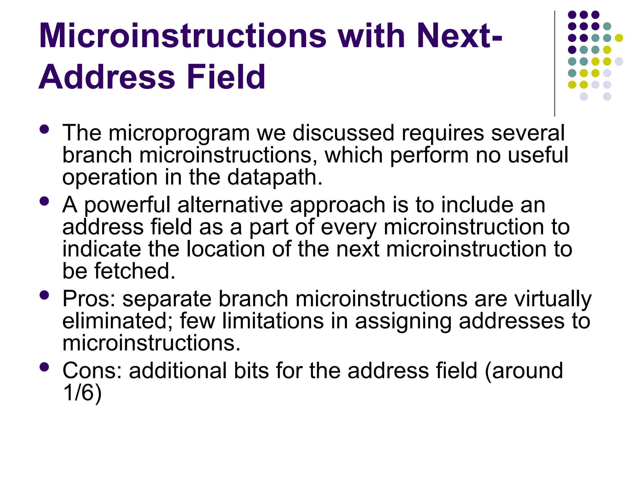
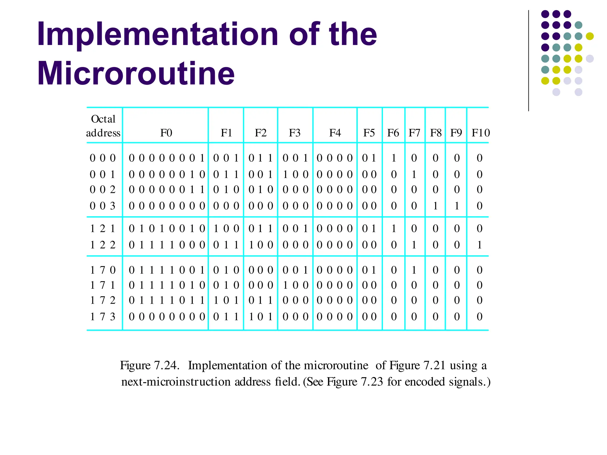
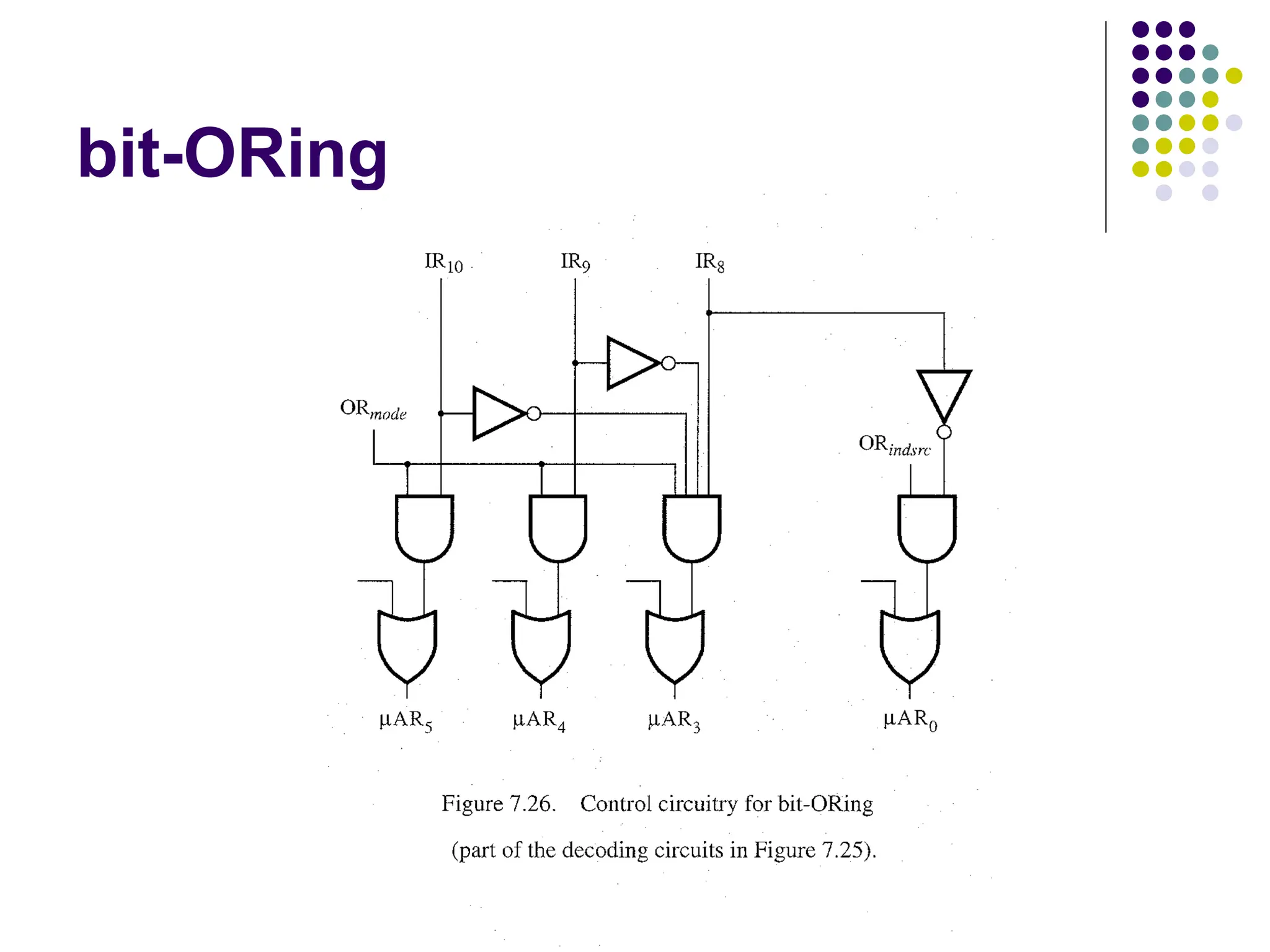
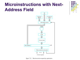
Microinstructions with Next-
AddressField
The microprogram we discussed requires several
branch microinstructions, which perform no useful
operation in the datapath.
A powerful alternative approach is to include an
address field as a part of every microinstruction to
indicate the location of the next microinstruction to
be fetched.
Pros: separate branch microinstructions are virtually
eliminated; few limitations in assigning addresses to
microinstructions.
Cons: additional bits for the address field (around
1/6)
52.
Microinstructions with Next-
AddressField
Figure 7.22. Microinstruction-sequencing organization.
Condition
codes
IR
Decoding circuits
Control store
Next address
Microinstruction decoder
Control signals
Inputs
External
AR
IR
53.
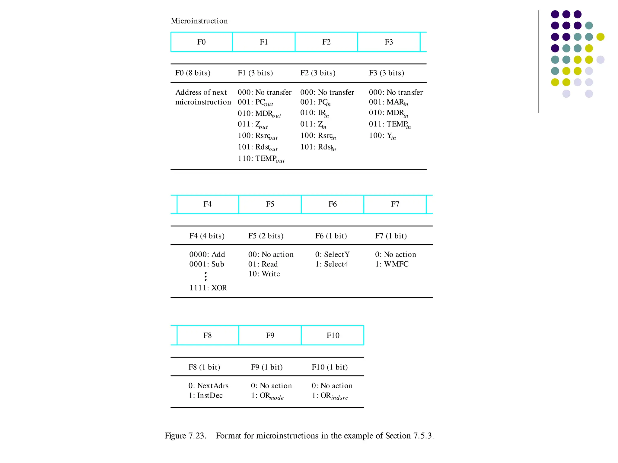
F1 (3 bits)
000:No transfer
001: PCout
010: MDRout
011: Zout
100: Rsrc
out
101: Rdstout
110: TEMPout
F0 F1 F2 F3
F0 (8 bits) F2 (3 bits) F3 (3 bits)
000: No transfer
001: PC
in
010: IR
in
011: Zin
100: Rsrc
in
000: No transfer
001: MARin
F4 F5 F6 F7
F5 (2 bits)
F4 (4 bits) F6 (1 bit)
0000: Add
0001: Sub
0: SelectY
1: Select4
00: No action
01: Read
Microinstruction
Address of next
microinstruction
101: Rdstin
010: MDRin
011: TEMP
in
100: Yin
1111: XOR
10: Write
F8 F9 F10
F8 (1 bit)
F7 (1 bit)
F9 (1 bit) F10 (1 bit)
0: No action
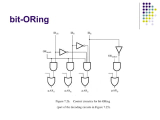
1: WMFC
0: No action
1: ORindsrc
0: No action
1: ORmode
0: NextAdrs
1: InstDec
Figure 7.23. Format for microinstructions in the example of Section 7.5.3.
decoder
Microinstruction
Control store
Next addressF1 F2
Other control signals
F10
F9
F8
Decoder
Decoder
circuits
Decoding
Condition
External
codes
inputs
Rsrc Rdst
IR
Rdstout
Rdstin
Rsrcout
Rsrcin
AR
InstDecout
ORmode
ORindsrc
R15in R15out R0in R0out
Figure 7.25. Some details of the control-signal-generating circuitry.


![Executing an Instruction
Fetch the contents of the memory location pointed
to by the PC. The contents of this location are
loaded into the IR (fetch phase).
IR ← [[PC]]
Assuming that the memory is byte addressable,
increment the contents of the PC by 4 (fetch phase).
PC ← [PC] + 4
Carry out the actions specified by the instruction in
the IR (execution phase).](https://image.slidesharecdn.com/unit6-basic-processing-unit-250730132304-96c5118e/85/unit_6-basic-processing-unit-pptt-engineering-5-320.jpg)


![3.Fetching a Word from
Memory
The response time of each memory access varies
(cache miss, memory-mapped I/O,…).
To accommodate this, the processor waits until it
receives an indication that the requested operation
has been completed (Memory-Function-Completed,
MFC).
Move (R1), R2
MAR ← [R1]
Start a Read operation on the memory bus
Wait for the MFC response from the memory
Load MDR from the memory bus
R2 ← [MDR]](https://image.slidesharecdn.com/unit6-basic-processing-unit-250730132304-96c5118e/85/unit_6-basic-processing-unit-pptt-engineering-19-320.jpg)


![OP code 0 1 0 Rsrc Rdst
Mode
Contents of IR
0
3
4
7
8
10
11
Figure 7.21. Microinstruction for Add (Rsrc)+,Rdst.
Note: Microinstruction at location 170 is not executed for this addressing mode.
Address Microinstruction
(octal)
000 PCout, MARin , Read, Select
4 , Add, Zin
001 Zout, PCin, Yin, WMFC
002 MDRout, IRin
003 Branch {
PC 101 (from Instruction decoder);
PC5,4 [IR10,9]; PC3
121 Rsrcout, MARin , Read, Select4, Add, Z
in
122 Zout , Rsrcin
123
170 MDRout, MARin , Read, WMFC
171 MDRout, Yin
172 Rdstout , SelectY
, Add, Zin
173 Zout , Rdstin, End
[IR10][IR9][IR8]}
Branch {PC 170;PC0 [IR8]}, WMFC
Textbook page 439](https://image.slidesharecdn.com/unit6-basic-processing-unit-250730132304-96c5118e/85/unit_6-basic-processing-unit-pptt-engineering-50-320.jpg)


![Executing an Instruction
Fetch the contents of the memory location pointed
to by the PC. The contents of this location are
loaded into the IR (fetch phase).
IR ← [[PC]]
Assuming that the memory is byte addressable,
increment the contents of the PC by 4 (fetch phase).
PC ← [PC] + 4
Carry out the actions specified by the instruction in
the IR (execution phase).](https://image.slidesharecdn.com/unit6-basic-processing-unit-250730132304-96c5118e/75/unit_6-basic-processing-unit-pptt-engineering-5-2048.jpg)


![3.Fetching a Word from
Memory
The response time of each memory access varies
(cache miss, memory-mapped I/O,…).
To accommodate this, the processor waits until it
receives an indication that the requested operation
has been completed (Memory-Function-Completed,
MFC).
Move (R1), R2
MAR ← [R1]
Start a Read operation on the memory bus
Wait for the MFC response from the memory
Load MDR from the memory bus
R2 ← [MDR]](https://image.slidesharecdn.com/unit6-basic-processing-unit-250730132304-96c5118e/75/unit_6-basic-processing-unit-pptt-engineering-19-2048.jpg)


![OP code 0 1 0 Rsrc Rdst
Mode
Contents of IR
0
3
4
7
8
10
11
Figure 7.21. Microinstruction for Add (Rsrc)+,Rdst.
Note: Microinstruction at location 170 is not executed for this addressing mode.
Address Microinstruction
(octal)
000 PCout, MARin , Read, Select
4 , Add, Zin
001 Zout, PCin, Yin, WMFC
002 MDRout, IRin
003 Branch {
PC 101 (from Instruction decoder);
PC5,4 [IR10,9]; PC3
121 Rsrcout, MARin , Read, Select4, Add, Z
in
122 Zout , Rsrcin
123
170 MDRout, MARin , Read, WMFC
171 MDRout, Yin
172 Rdstout , SelectY
, Add, Zin
173 Zout , Rdstin, End
[IR10][IR9][IR8]}
Branch {PC 170;PC0 [IR8]}, WMFC
Textbook page 439](https://image.slidesharecdn.com/unit6-basic-processing-unit-250730132304-96c5118e/75/unit_6-basic-processing-unit-pptt-engineering-50-2048.jpg)