Download to read offline

![P.Kanaka Sirisha.et al. Int. Journal of Engineering Research and Applications www.ijera.com
ISSN: 2248-9622, Vol. 6, Issue 4, (Part - 2) April 2016, pp.42-45
www.ijera.com 44|P a g e
the DR is always readily available to the system
bus that connects various blocks of the processor.
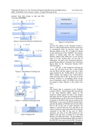
Fig 3:
As the architecture indicates, the output result of
the ALU is again stored in the Accumulator (Acc)
itself or transferred to the System Bus based on the
Selection pin of the DeMUX2. The MUX present
selects the input to the Acc, either the data in the
System Bus or the ALU output and the data enters
‘Acc’ only when the ‘Load Acc’ is enabled. A
DeMUX1 is then present in order to share the data
in the Acc to either the input ‘A’ of the ALU or to
the System Bus as the output.The input ‘B’ to the
ALU is also provided by the System Bus itself.
When the input enters as ‘B’ from the System Bus,
the Input ‘A’ doesn’t change since the ‘Load Acc’
is disabled. Hence the operation is performed based
on the ALU Opcode provided by the Control Unit,
and the result of the Operation is stored again in the
‘Acc’ itself. The data in the ‘Acc’ can be used by
moving it into the System Bus by selecting the
appropriate DeMUX signal.
Fig 4:
The Register File (RF) of the CISC32 Processor
contains 4 General Purpose Registers each called
Apple (R1), IBM (R2), INTEL (R3) and
MICROSOFT (R4). The System Bus attached to
the RF is used by the processor to both read and
write the RF. Operations ‘Read’ and ‘Write’
depend upon the ‘Read Enable (R_E)’ and ‘Write
Enable (W_E)’ Signals attached to the Register
File.
Fig 5:
The control Unit (CU) block consists of
two units named Decoding Unit (DU) and Timing
Unit (TU). The opcode that comes out of the FU1
acts as the input to the CU. The CU then enables
the necessary signals in a sequential manner to
perform the operation indicated by the opcode.
‘Heart’ to the Human Body is what ‘CU’ to the
program.
III. CISC INSTRUCTION FORMAT
1. Opcode:- It occupies 8 bits out of 32 bits,
which can accommodate a maximum of 28
(256) instructions.
2. The processor has 4 user accessible registers
and can be addressed by 2 bits, hence in case
of ‘register to register’ addressing; the entire
operation can be installed in a single
instruction.
3. In case ‘memory memory’ or‘memory to
register’ operations 2 to words
IV. EXECUTION CYCLE
FETCH INSTRUCTION: -At First, the instruction
will be fetched from the program memory through
the bus allocated to it. The instruction is then stored
in an instruction queue and there on to be passed to
the Control Unit.
Decode: -The instruction will be decoded in the
decode unit of control unit and the necessary enable
and disable signals will be sent to the necessary
blocks (Micro programmed Control Unit) using the
timing unit. The operands, if present, are placed on
to the Internal Data Bus for the use of the Registers
or ALU.
Fetch Operands: -If the opcode requests fetching
of operands from data memory, the memory
location will be placed on to the internal bus so that
the location will be copied on to the Data Memory
PC and then to the bus attached to the Data
Memory. The Operand will be fetched and placed
on the Internal Data Bus making it available for the
ALU or the Register Bank as in the previous case.
Execute: -The processor then performs the
operation indicated by the opcode.
Store Output Operand: -It then stores the result in
the Accumulator (By Default; if it is an ALU
Operation). Thus the ‘Execution Cycle’ is
completed.
V. CONCLUSIONS
• The CISC32 Processor is implemented using
Verilog Language.
• The Processor is designed using Harvard
Architecture and hence uses two Different
Program Counters are used in CISC32
Processor to point the Program Memory and
Data Memory Individually.
• The speed of the processor is 1 MHz
• The Accumulator Type Instruction Set
Architecture (ISA) is used in the CISC32
Processor (Where the result is stored in Acc
itself).
• Up to 256 different instructions are
compatible.
• 3 types of addressing modes are used in the
processor.
• 5 General Purpose Registers are used
(including Accumulator).
• Instruction Queuing is also made available
which slightly increases the speed of the
processor Operations.
REFERENCES
[1]. Computer Organization and Architecture’
by Prof. J. K. Deka, IIT- Guwahati
[2]. Computer Organization and Architecture’
by William Stallings](https://image.slidesharecdn.com/h0604024245-160728092713/85/Verilog-Implementation-of-32-Bit-CISC-Processor-3-320.jpg)
![P.Kanaka Sirisha.et al. Int. Journal of Engineering Research and Applications www.ijera.com
ISSN: 2248-9622, Vol. 6, Issue 4, (Part - 2) April 2016, pp.42-45
www.ijera.com 45|P a g e
[3]. Hasan Krad and Aws Yousif Al-Taie, ‘A
New Trend for CISC and RISC
Architectures’, IEEE.
[4]. A journal on 8 Bit RISC processor using
verilog HDL](https://image.slidesharecdn.com/h0604024245-160728092713/85/Verilog-Implementation-of-32-Bit-CISC-Processor-4-320.jpg)

![P.Kanaka Sirisha.et al. Int. Journal of Engineering Research and Applications www.ijera.com
ISSN: 2248-9622, Vol. 6, Issue 4, (Part - 2) April 2016, pp.42-45
www.ijera.com 44|P a g e
the DR is always readily available to the system
bus that connects various blocks of the processor.
Fig 3:
As the architecture indicates, the output result of
the ALU is again stored in the Accumulator (Acc)
itself or transferred to the System Bus based on the
Selection pin of the DeMUX2. The MUX present
selects the input to the Acc, either the data in the
System Bus or the ALU output and the data enters
‘Acc’ only when the ‘Load Acc’ is enabled. A
DeMUX1 is then present in order to share the data
in the Acc to either the input ‘A’ of the ALU or to
the System Bus as the output.The input ‘B’ to the
ALU is also provided by the System Bus itself.
When the input enters as ‘B’ from the System Bus,
the Input ‘A’ doesn’t change since the ‘Load Acc’
is disabled. Hence the operation is performed based
on the ALU Opcode provided by the Control Unit,
and the result of the Operation is stored again in the
‘Acc’ itself. The data in the ‘Acc’ can be used by
moving it into the System Bus by selecting the
appropriate DeMUX signal.
Fig 4:
The Register File (RF) of the CISC32 Processor
contains 4 General Purpose Registers each called
Apple (R1), IBM (R2), INTEL (R3) and
MICROSOFT (R4). The System Bus attached to
the RF is used by the processor to both read and
write the RF. Operations ‘Read’ and ‘Write’
depend upon the ‘Read Enable (R_E)’ and ‘Write
Enable (W_E)’ Signals attached to the Register
File.
Fig 5:
The control Unit (CU) block consists of
two units named Decoding Unit (DU) and Timing
Unit (TU). The opcode that comes out of the FU1
acts as the input to the CU. The CU then enables
the necessary signals in a sequential manner to
perform the operation indicated by the opcode.
‘Heart’ to the Human Body is what ‘CU’ to the
program.
III. CISC INSTRUCTION FORMAT
1. Opcode:- It occupies 8 bits out of 32 bits,
which can accommodate a maximum of 28
(256) instructions.
2. The processor has 4 user accessible registers
and can be addressed by 2 bits, hence in case
of ‘register to register’ addressing; the entire
operation can be installed in a single
instruction.
3. In case ‘memory memory’ or‘memory to
register’ operations 2 to words
IV. EXECUTION CYCLE
FETCH INSTRUCTION: -At First, the instruction
will be fetched from the program memory through
the bus allocated to it. The instruction is then stored
in an instruction queue and there on to be passed to
the Control Unit.
Decode: -The instruction will be decoded in the
decode unit of control unit and the necessary enable
and disable signals will be sent to the necessary
blocks (Micro programmed Control Unit) using the
timing unit. The operands, if present, are placed on
to the Internal Data Bus for the use of the Registers
or ALU.
Fetch Operands: -If the opcode requests fetching
of operands from data memory, the memory
location will be placed on to the internal bus so that
the location will be copied on to the Data Memory
PC and then to the bus attached to the Data
Memory. The Operand will be fetched and placed
on the Internal Data Bus making it available for the
ALU or the Register Bank as in the previous case.
Execute: -The processor then performs the
operation indicated by the opcode.
Store Output Operand: -It then stores the result in
the Accumulator (By Default; if it is an ALU
Operation). Thus the ‘Execution Cycle’ is
completed.
V. CONCLUSIONS
• The CISC32 Processor is implemented using
Verilog Language.
• The Processor is designed using Harvard
Architecture and hence uses two Different
Program Counters are used in CISC32
Processor to point the Program Memory and
Data Memory Individually.
• The speed of the processor is 1 MHz
• The Accumulator Type Instruction Set
Architecture (ISA) is used in the CISC32
Processor (Where the result is stored in Acc
itself).
• Up to 256 different instructions are
compatible.
• 3 types of addressing modes are used in the
processor.
• 5 General Purpose Registers are used
(including Accumulator).
• Instruction Queuing is also made available
which slightly increases the speed of the
processor Operations.
REFERENCES
[1]. Computer Organization and Architecture’
by Prof. J. K. Deka, IIT- Guwahati
[2]. Computer Organization and Architecture’
by William Stallings](https://image.slidesharecdn.com/h0604024245-160728092713/75/Verilog-Implementation-of-32-Bit-CISC-Processor-3-2048.jpg)
![P.Kanaka Sirisha.et al. Int. Journal of Engineering Research and Applications www.ijera.com
ISSN: 2248-9622, Vol. 6, Issue 4, (Part - 2) April 2016, pp.42-45
www.ijera.com 45|P a g e
[3]. Hasan Krad and Aws Yousif Al-Taie, ‘A
New Trend for CISC and RISC
Architectures’, IEEE.
[4]. A journal on 8 Bit RISC processor using
verilog HDL](https://image.slidesharecdn.com/h0604024245-160728092713/75/Verilog-Implementation-of-32-Bit-CISC-Processor-4-2048.jpg)

The document presents the design and simulation of a 32-bit CISC processor using Verilog, focusing on its features such as Harvard architecture, instruction queuing, and support for various addressing modes. The processor is capable of executing a rich set of complex instructions and utilizes two distinct program counters for program and data memory, improving speed. It can accommodate up to 256 instructions and incorporates 5 general-purpose registers, with an operational speed of 1 MHz.


![4bit pc report[cse 08-section-b2_group-02]](https://cdn.slidesharecdn.com/ss_thumbnails/4bitpcreportcse-08section-b2group-02-150411124950-conversion-gate01-thumbnail.jpg?width=600ounds&width=560&fit=bounds)


