Download as PDF, PPTX


![Stack Pointer Register
Special register in I/O space [3E, 3D]
Enough bits to address data space
Initialized to RAMEND (address of highest memory address)
Instructions that use the stack pointer](https://image.slidesharecdn.com/lecture6-141008231245-conversion-gate01/85/AVR-arduino-dasar-23-320.jpg)
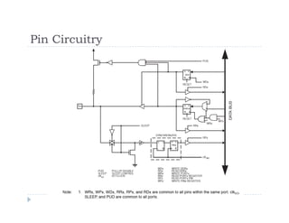
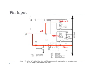
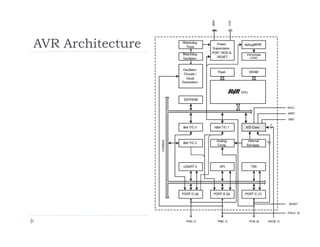
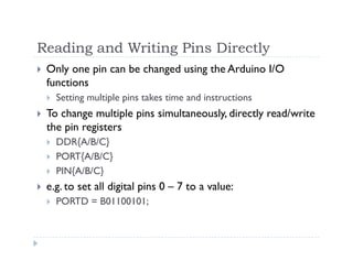
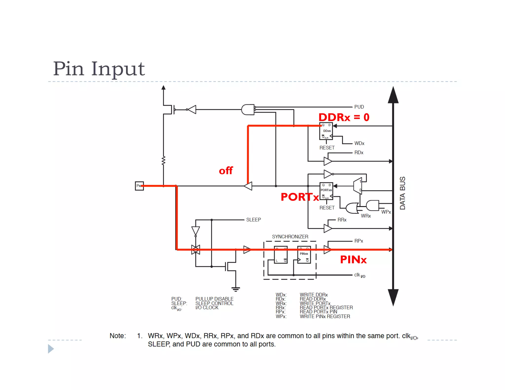
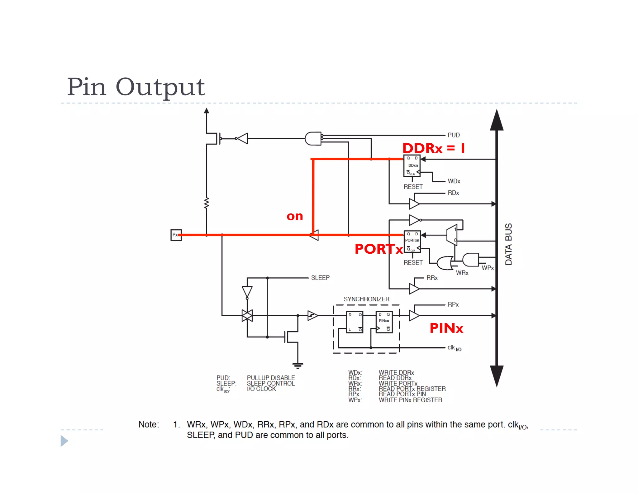
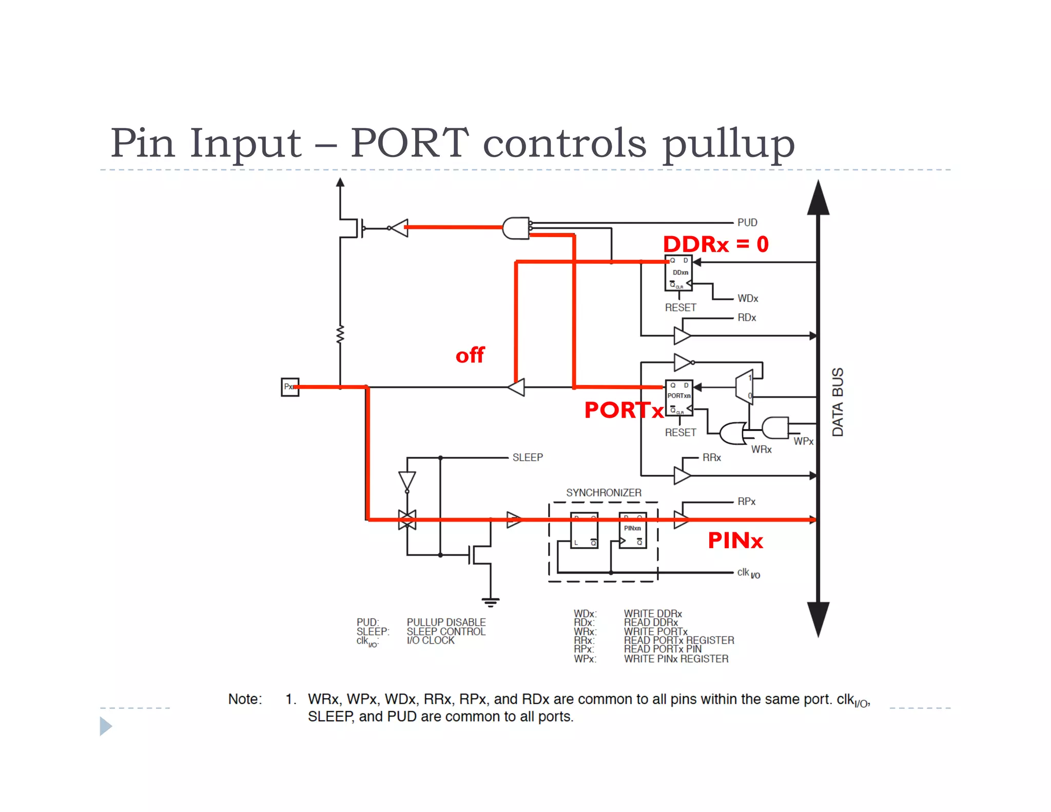
![Arduino Digital and Analog I/O Pins
Digital pins:
Pins 0 – 7: PORT D [0:7]
Pins 8 – 13: PORT B [0:5]
Pins 14 – 19: PORT C [0:5] (Arduino analog pins 0 – 5)
digital pins 0 and 1 are RX and TX for serial communication
digital pin 13 connected to the base board LED
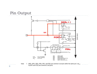
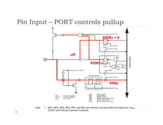
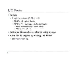
Digital Pin I/O Functions
pinMode(pin, mode)
Sets pin to INPUT or OUTPUT mode
Writes 1 bit in the DDRx register
digitalWrite(pin, value)
Sets pin value to LOW or HIGH (0 or 1)
Writes 1 bit in the PORTx register
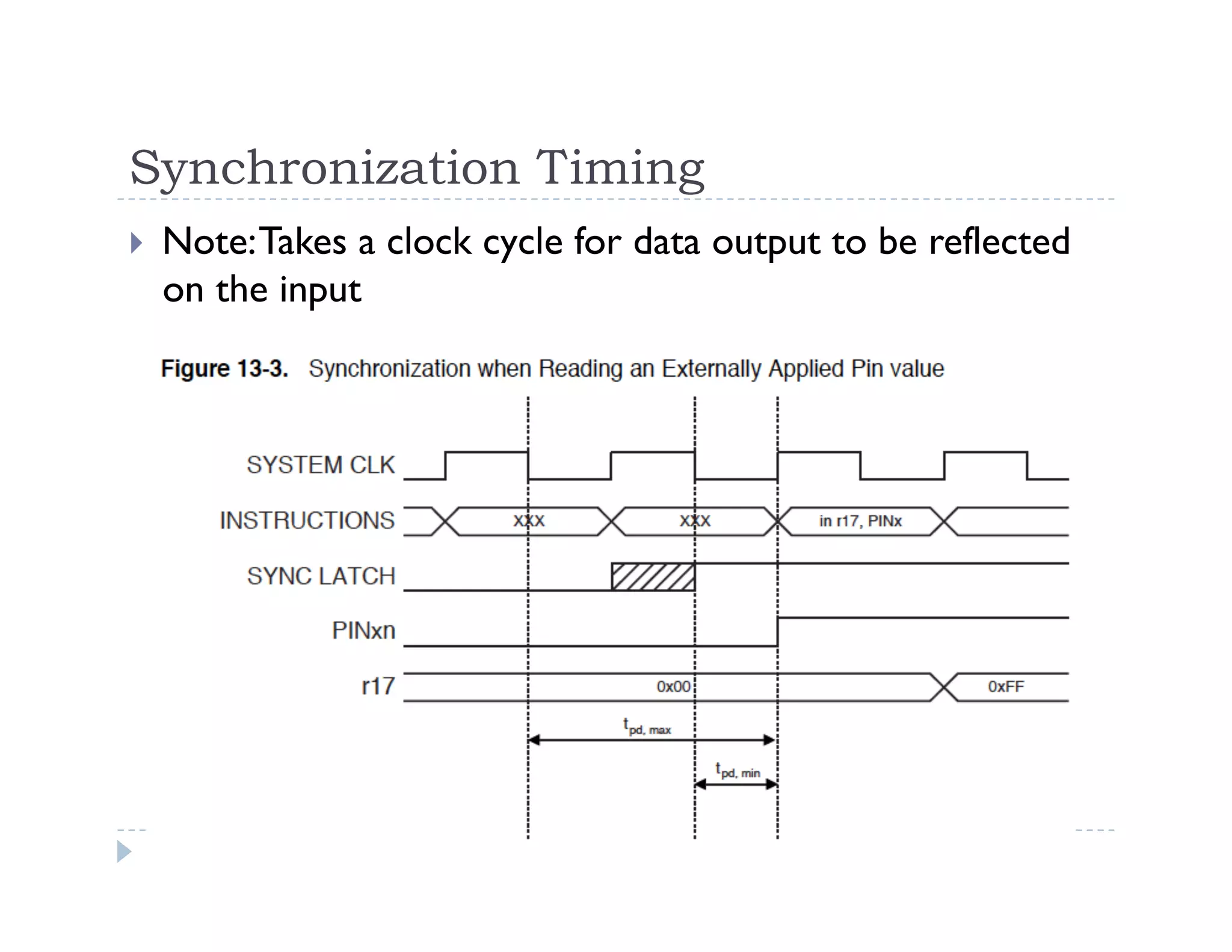
int value = digitalRead(pin)
Reads back pin value (0 or 1)
Read 1 bit in the PINx register](https://image.slidesharecdn.com/lecture6-141008231245-conversion-gate01/85/AVR-arduino-dasar-53-320.jpg)
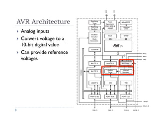


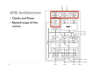
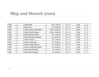
![Stack Pointer Register
Special register in I/O space [3E, 3D]
Enough bits to address data space
Initialized to RAMEND (address of highest memory address)
Instructions that use the stack pointer](https://image.slidesharecdn.com/lecture6-141008231245-conversion-gate01/75/AVR-arduino-dasar-23-2048.jpg)

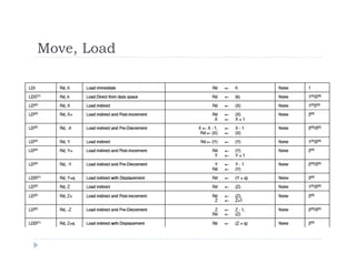
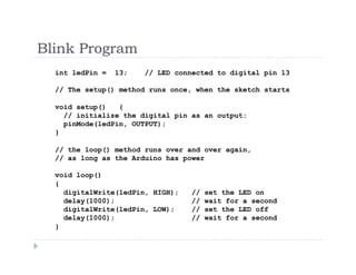
![Arduino Digital and Analog I/O Pins
Digital pins:
Pins 0 – 7: PORT D [0:7]
Pins 8 – 13: PORT B [0:5]
Pins 14 – 19: PORT C [0:5] (Arduino analog pins 0 – 5)
digital pins 0 and 1 are RX and TX for serial communication
digital pin 13 connected to the base board LED
Digital Pin I/O Functions
pinMode(pin, mode)
Sets pin to INPUT or OUTPUT mode
Writes 1 bit in the DDRx register
digitalWrite(pin, value)
Sets pin value to LOW or HIGH (0 or 1)
Writes 1 bit in the PORTx register
int value = digitalRead(pin)
Reads back pin value (0 or 1)
Read 1 bit in the PINx register](https://image.slidesharecdn.com/lecture6-141008231245-conversion-gate01/75/AVR-arduino-dasar-53-2048.jpg)

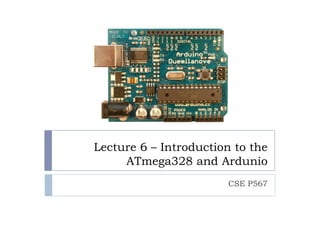
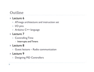
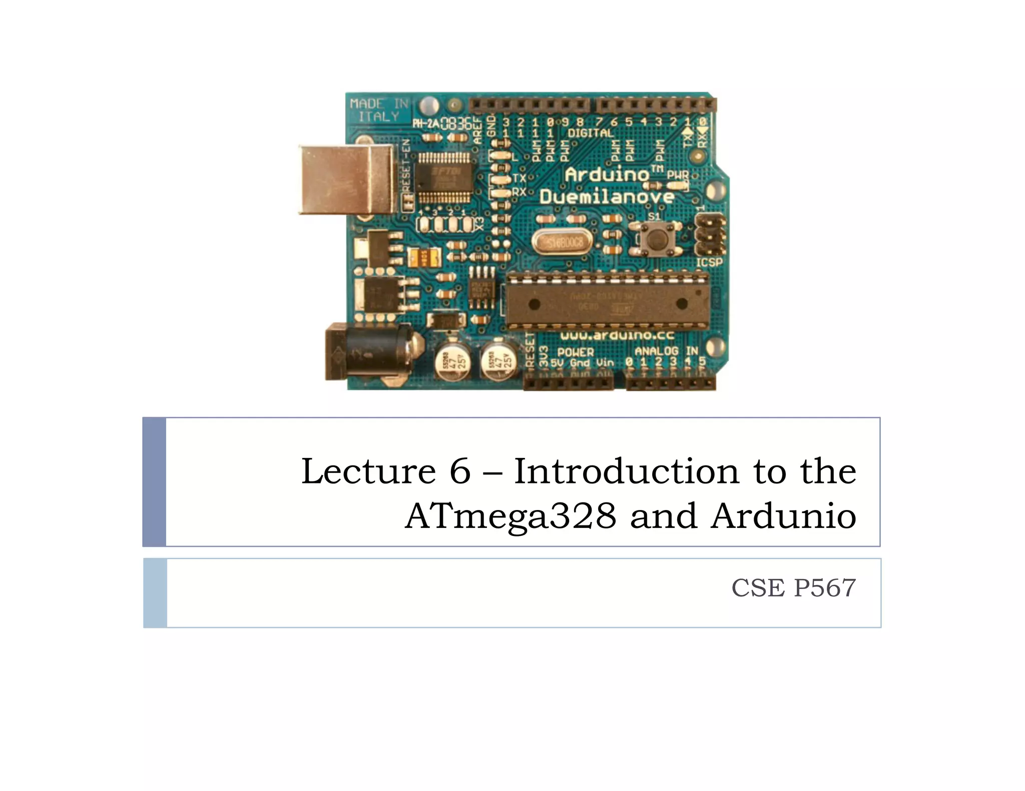
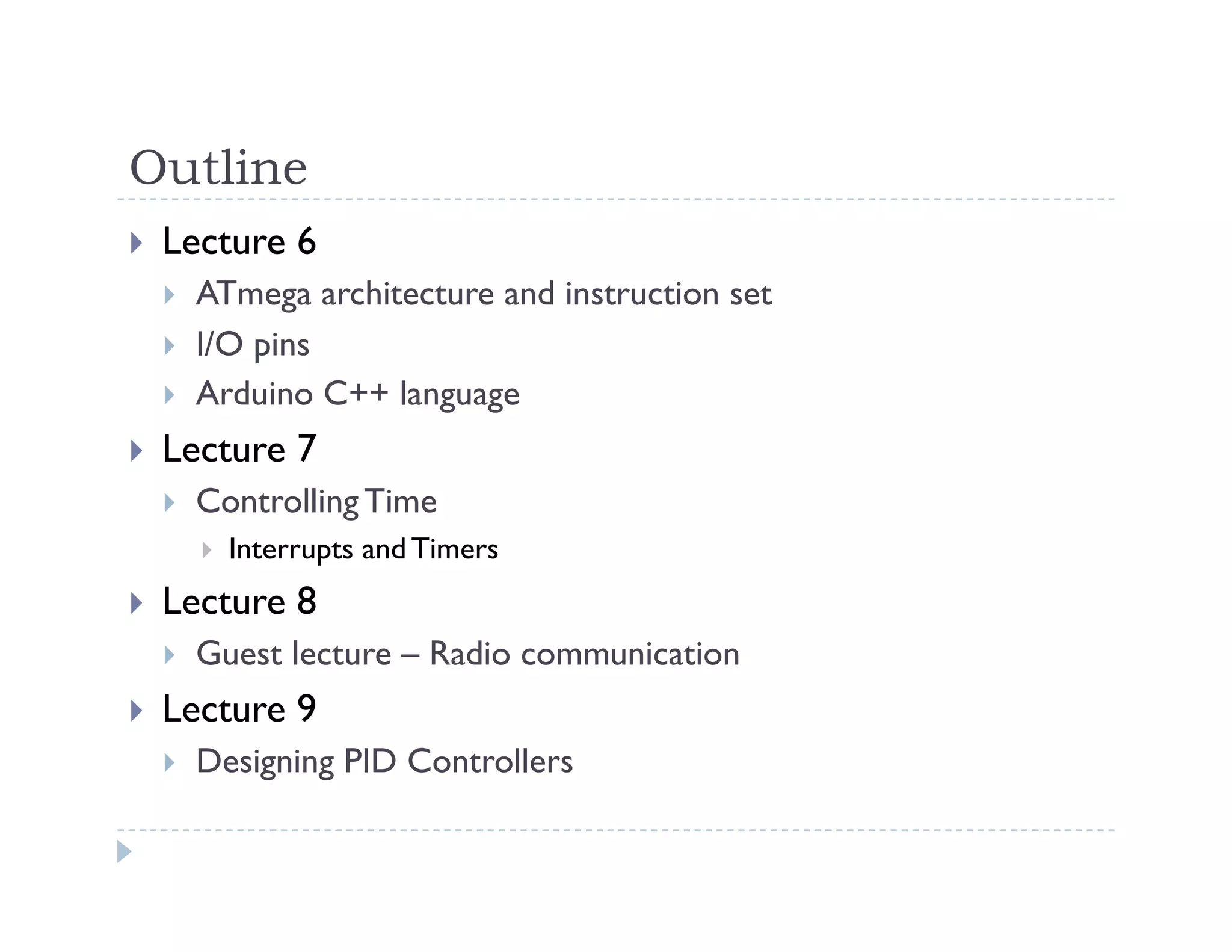
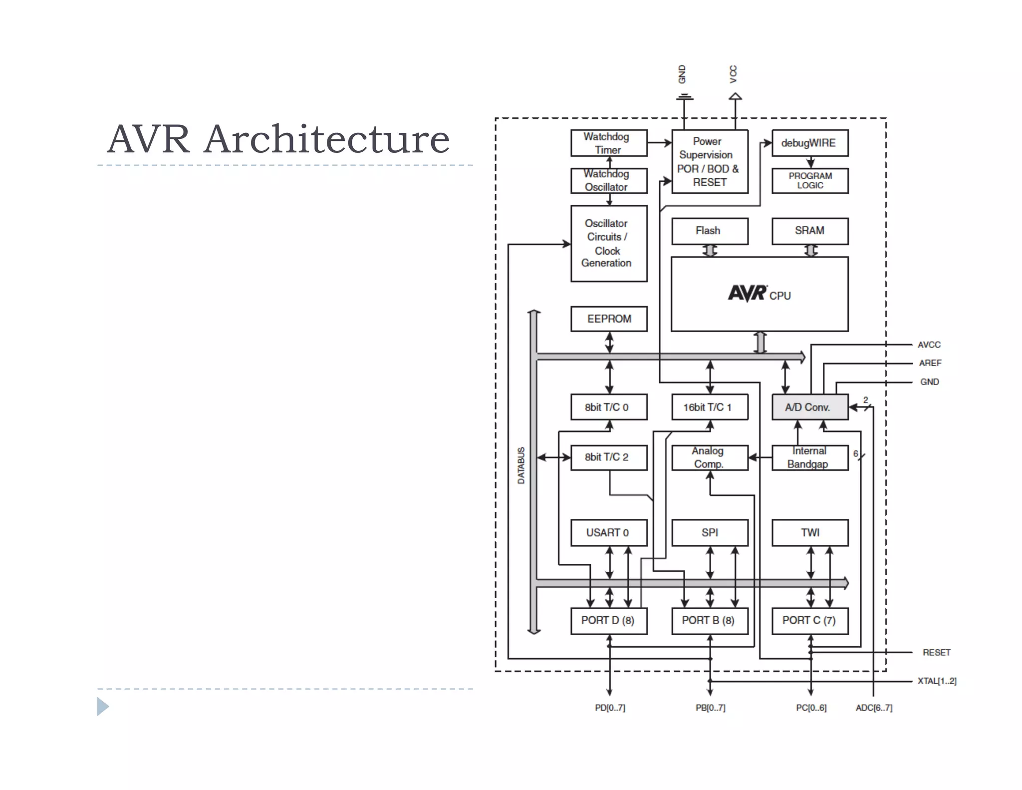
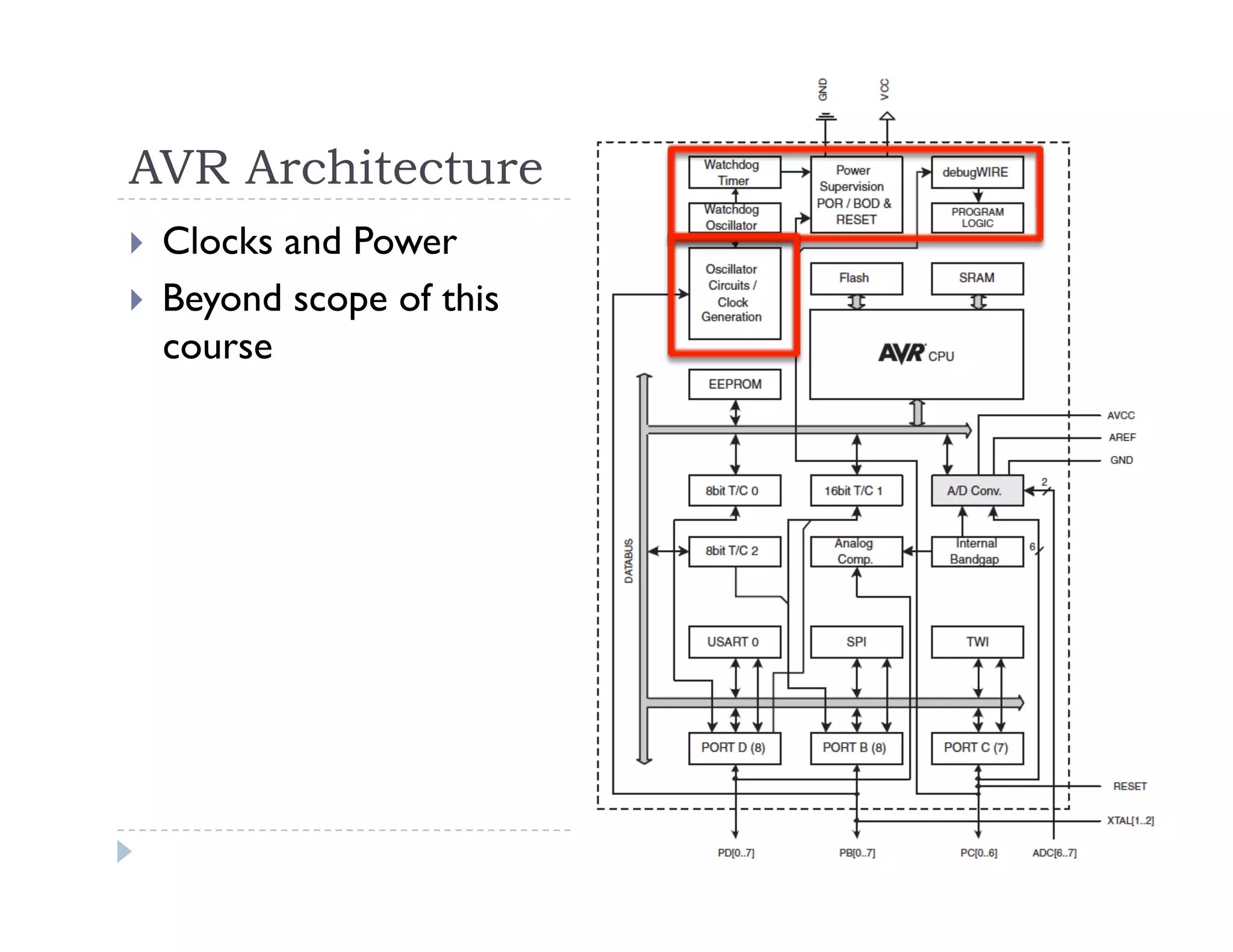
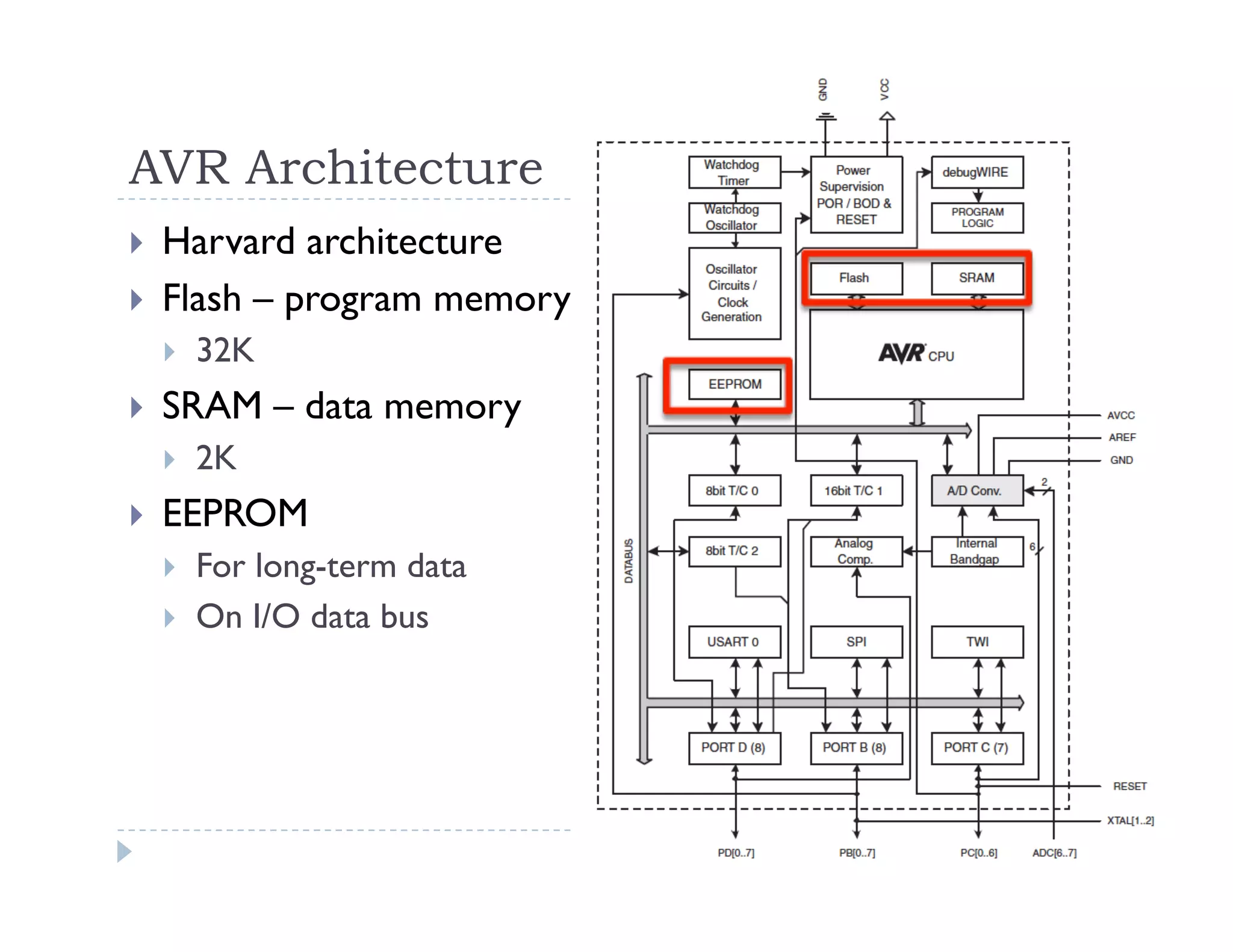
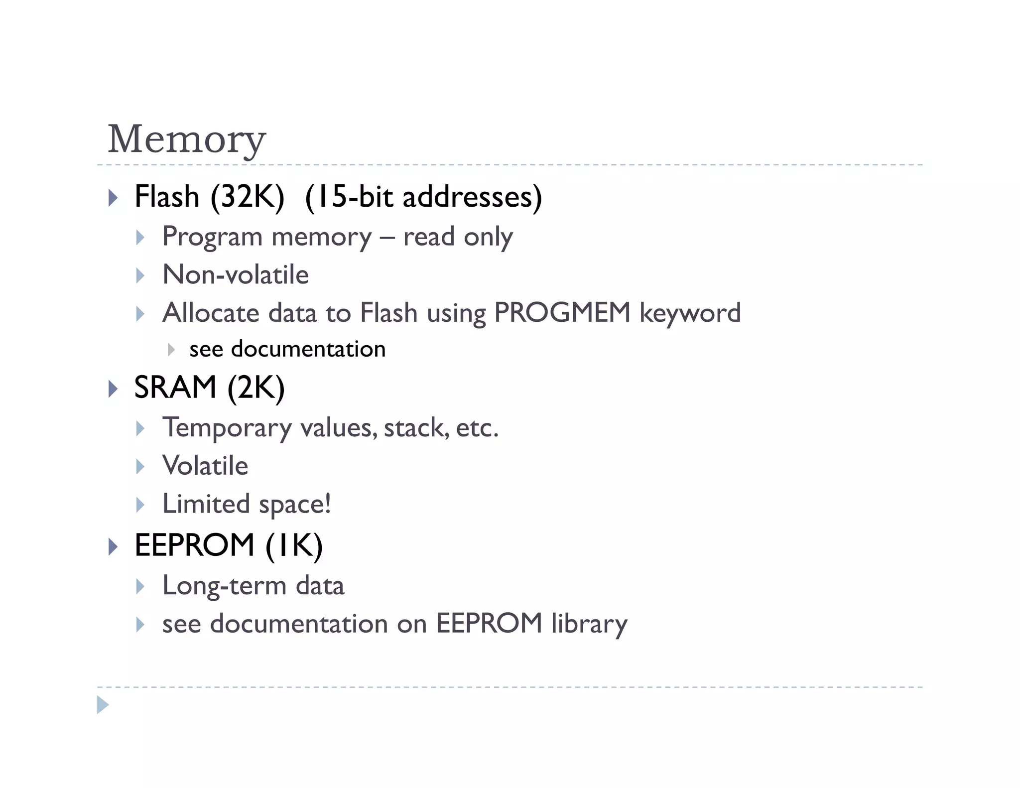
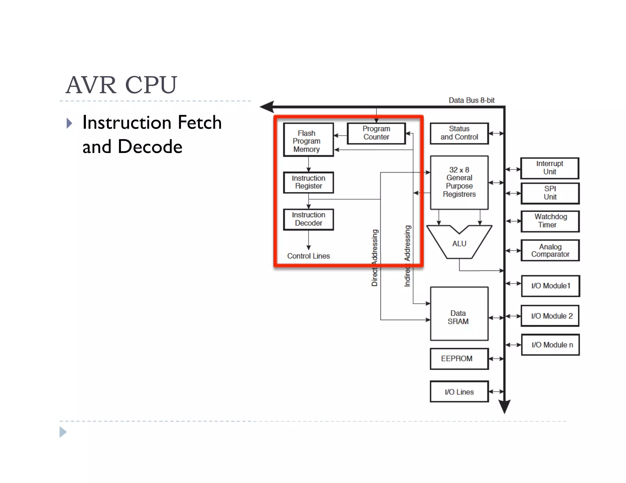
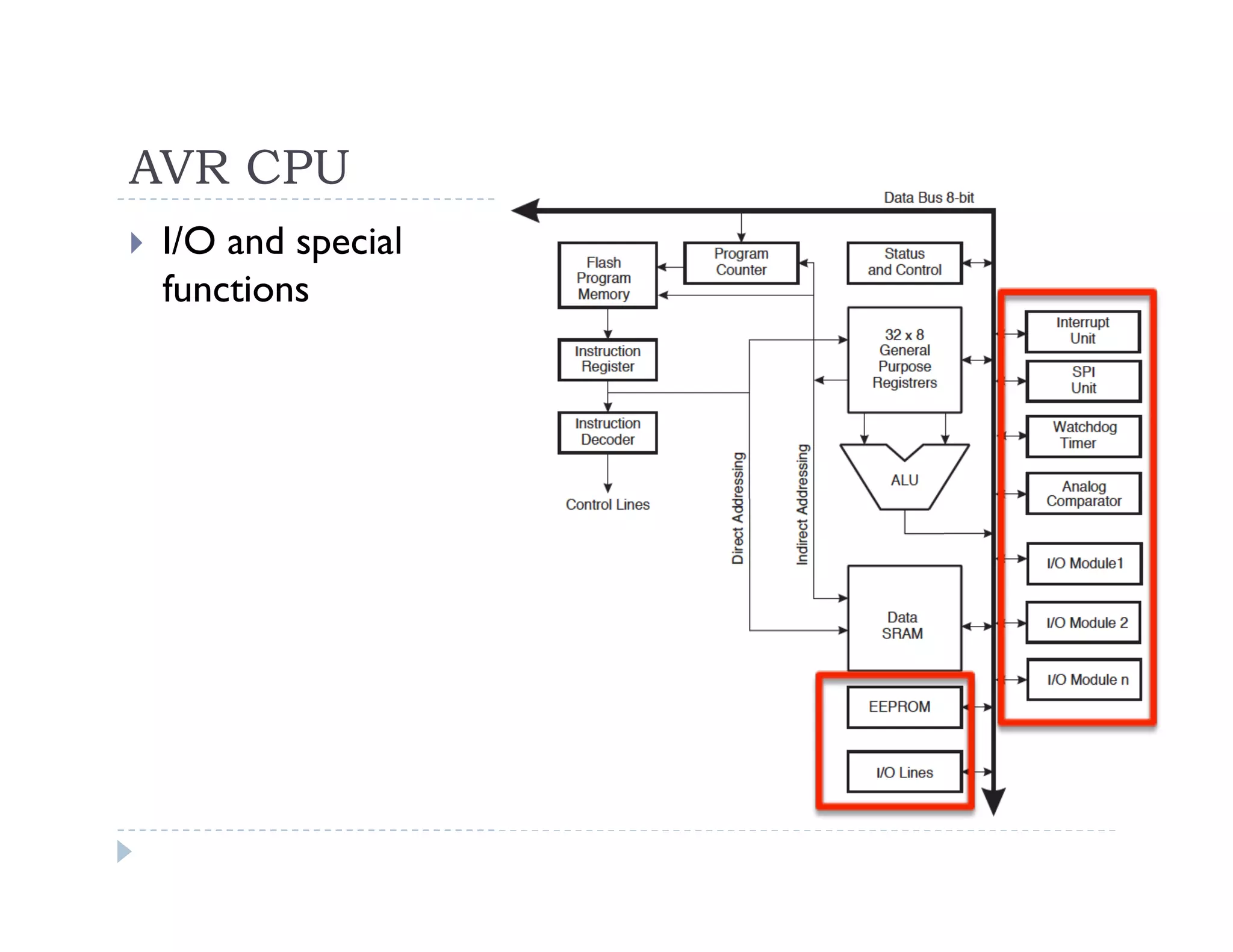
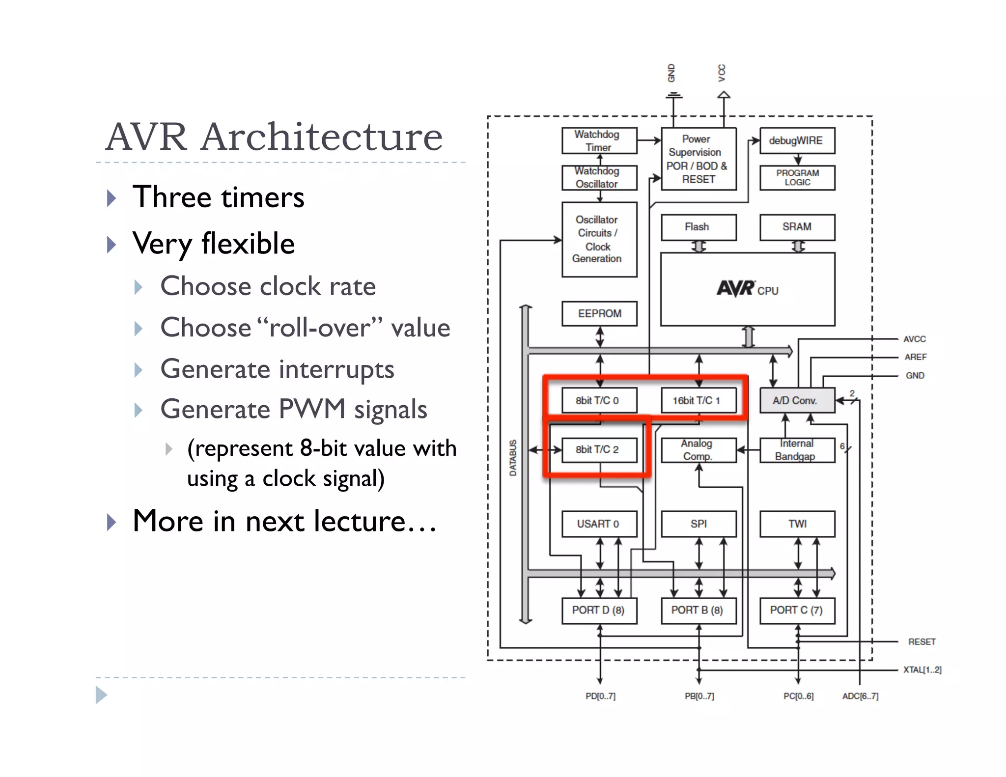
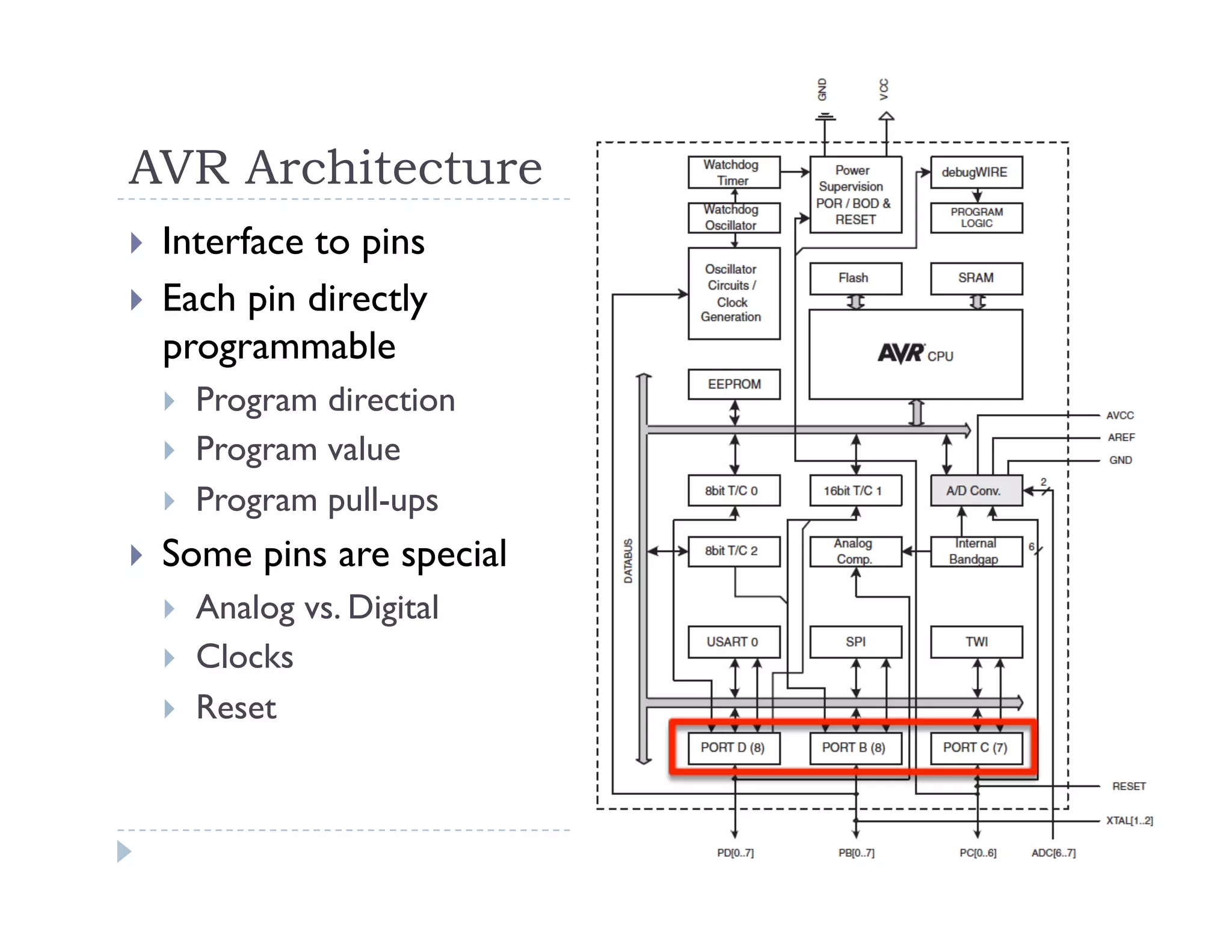
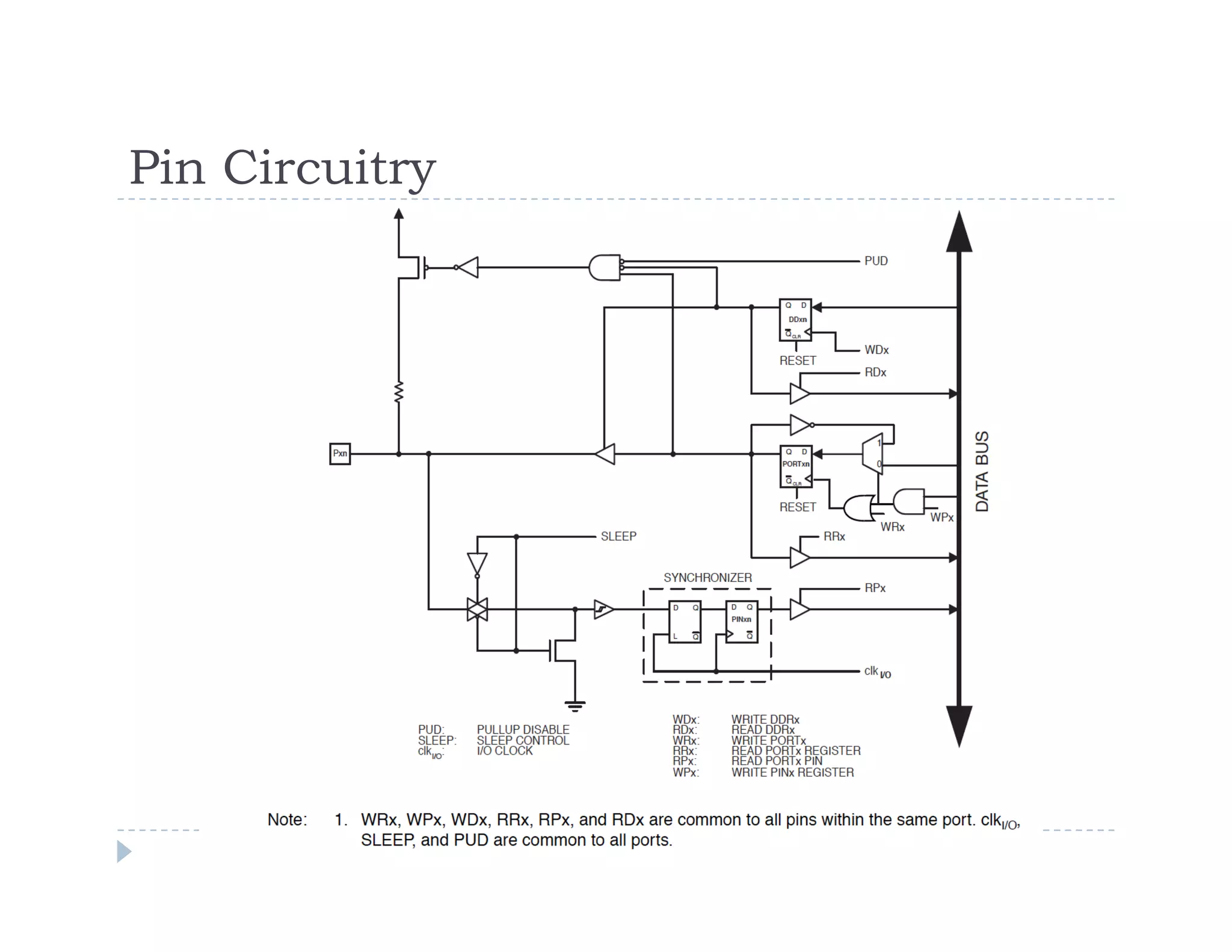
This document provides an overview of the topics that will be covered in lectures 6-9 of a course on the ATmega328 microcontroller and Arduino. Lecture 6 will introduce the ATmega architecture, instruction set, I/O pins, and the Arduino programming language. Lecture 7 will cover controlling time with interrupts and timers. Lecture 8 will include a guest lecture on radio communication. Lecture 9 will discuss designing PID controllers. The document then provides details on the ATmega328 architecture, memory, registers, instruction set, I/O interfaces and Arduino programming.


