2
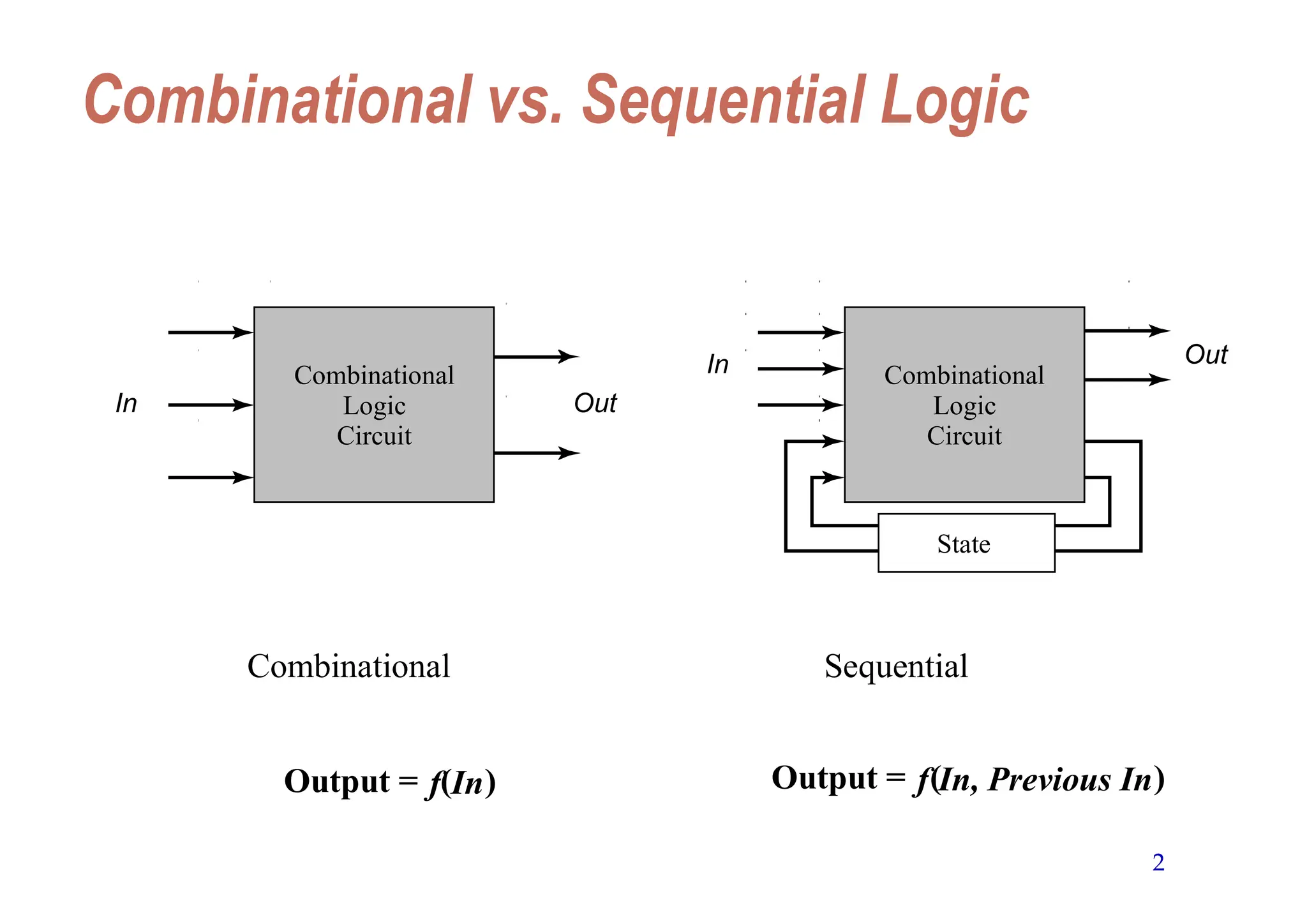
Combinational vs. SequentialLogic
Combinational Sequential
Output = f(In) Output = f(In, Previous In)
Combinational
Logic
Circuit
Out
In
Combinational
Logic
Circuit
Out
In
State
3.
3
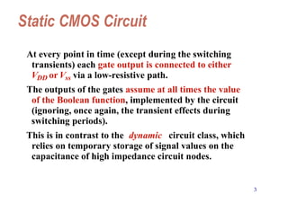
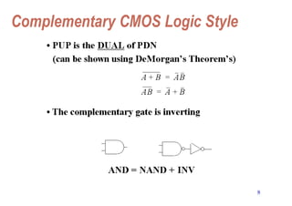
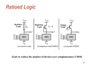
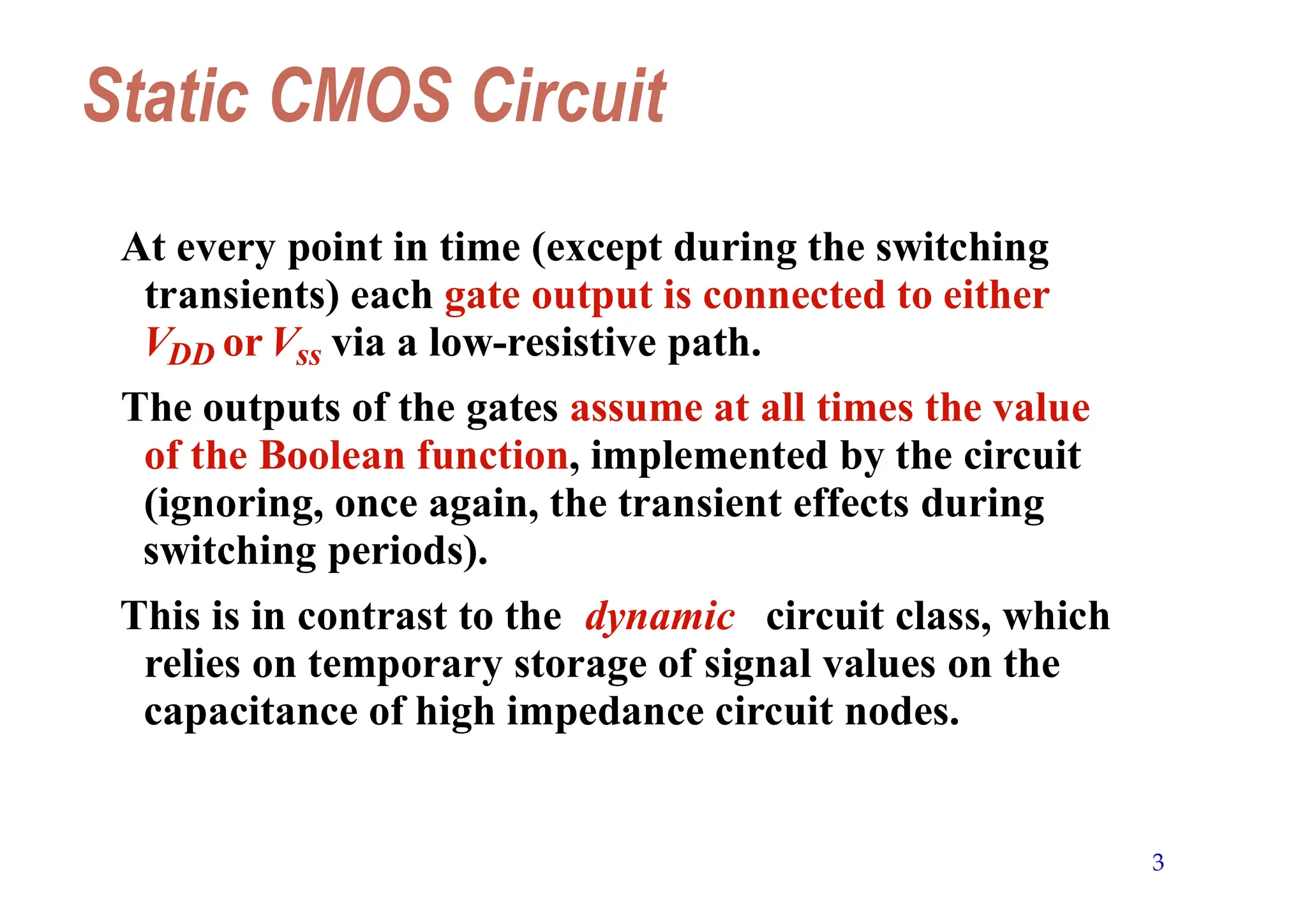
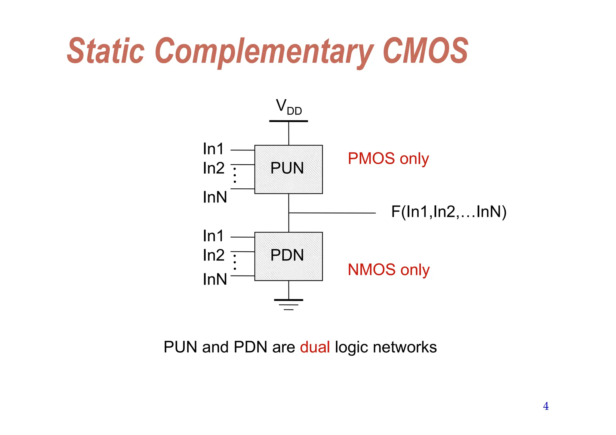
Static CMOS Circuit
Atevery point in time (except during the switching
transients) each gate output is connected to either
VDD orVss via a low-resistive path.
The outputs of the gates assume at all times the value
of the Boolean function, implemented by the circuit
(ignoring, once again, the transient effects during
switching periods).
This is in contrast to the dynamic circuit class, which
relies on temporary storage of signal values on the
capacitance of high impedance circuit nodes.
5
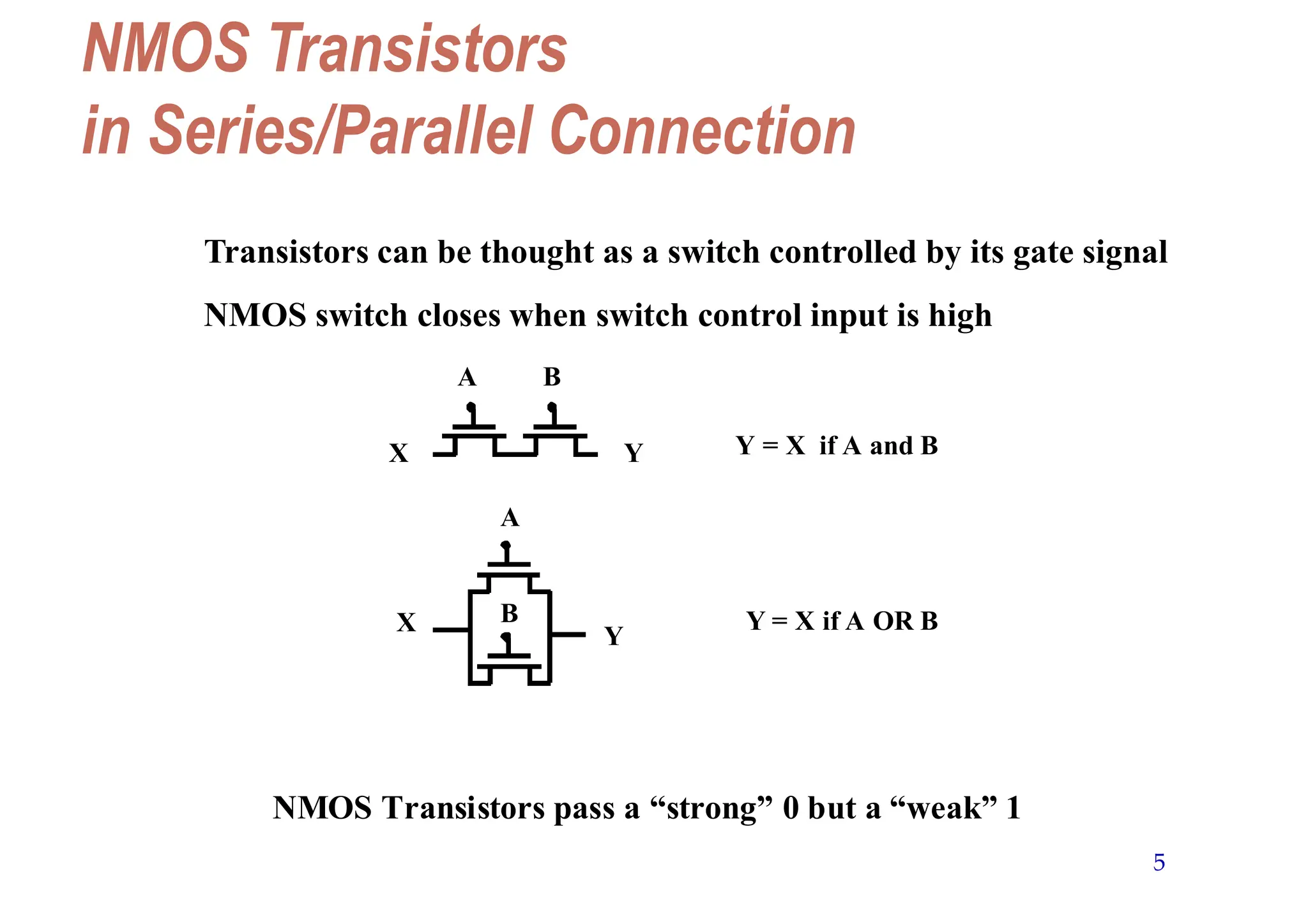
NMOS Transistors
in Series/ParallelConnection
Transistors can be thought as a switch controlled by its gate signal
NMOS switch closes when switch control input is high
X Y
A B
Y = X if A and B
X
Y
A
B Y = X if A OR B
NMOS Transistors pass a “strong” 0 but a “weak” 1
6.
6
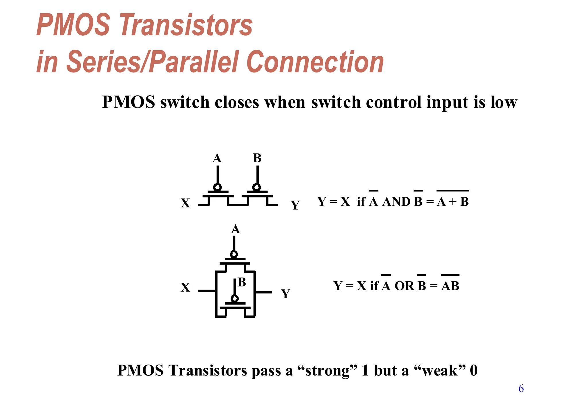
PMOS Transistors
in Series/ParallelConnection
X Y
A B
Y = X if A AND B = A + B
X Y
A
B Y = X if A OR B = AB
PMOS Transistors pass a “strong” 1 but a “weak” 0
PMOS switch closes when switch control input is low
7.
7
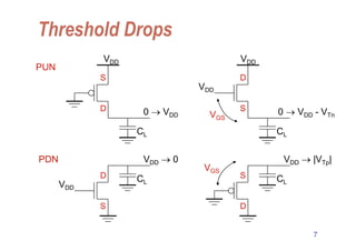
Threshold Drops
VDD
VDD 0
PDN
0 VDD
CL
CL
PUN
VDD
0 VDD - VTn
CL
VDD
VDD
VDD |VTp|
CL
S
D S
D
VGS
S
S
D
D
VGS
12
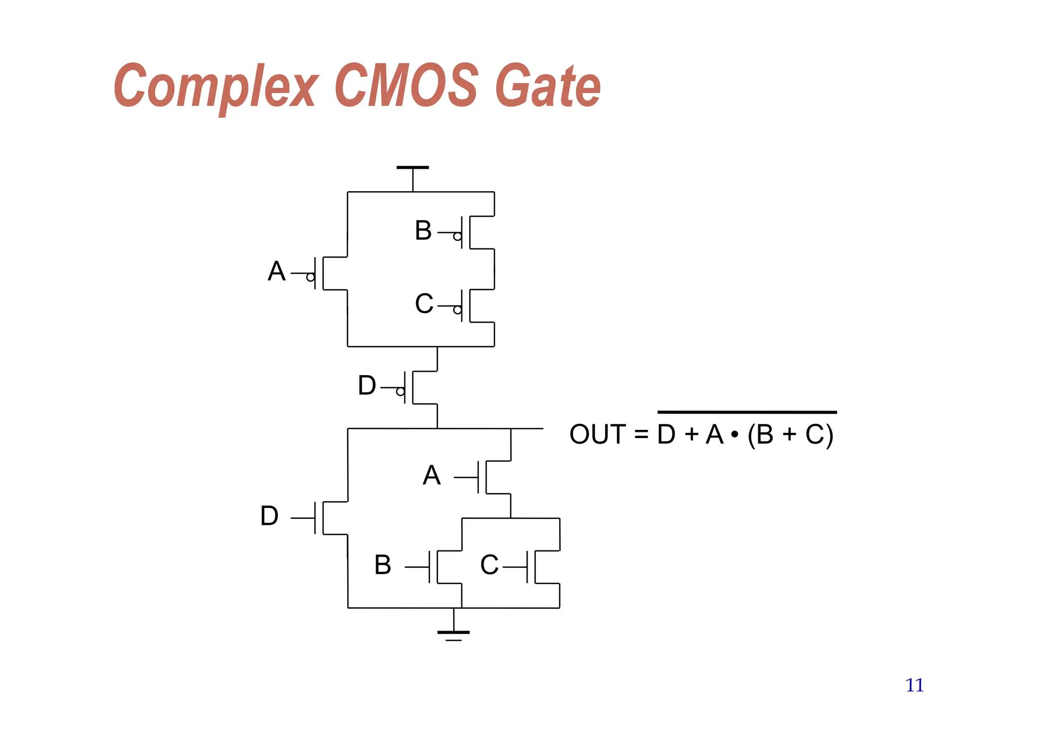
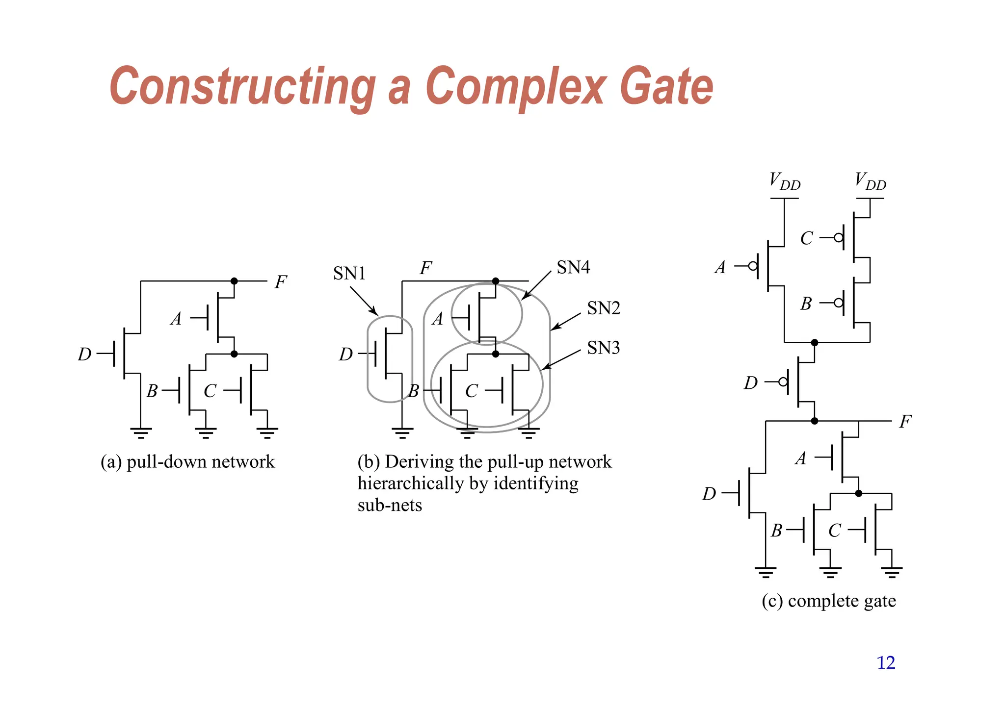
Constructing a ComplexGate
C
(a) pull-down network
SN1 SN4
SN2
SN3
D
F
F
A
D
B
C
D
F
A
B
C
(b) Deriving the pull-up network
hierarchically by identifying
sub-nets
D
A
A
B
C
VDD VDD
B
(c) complete gate
13.
13
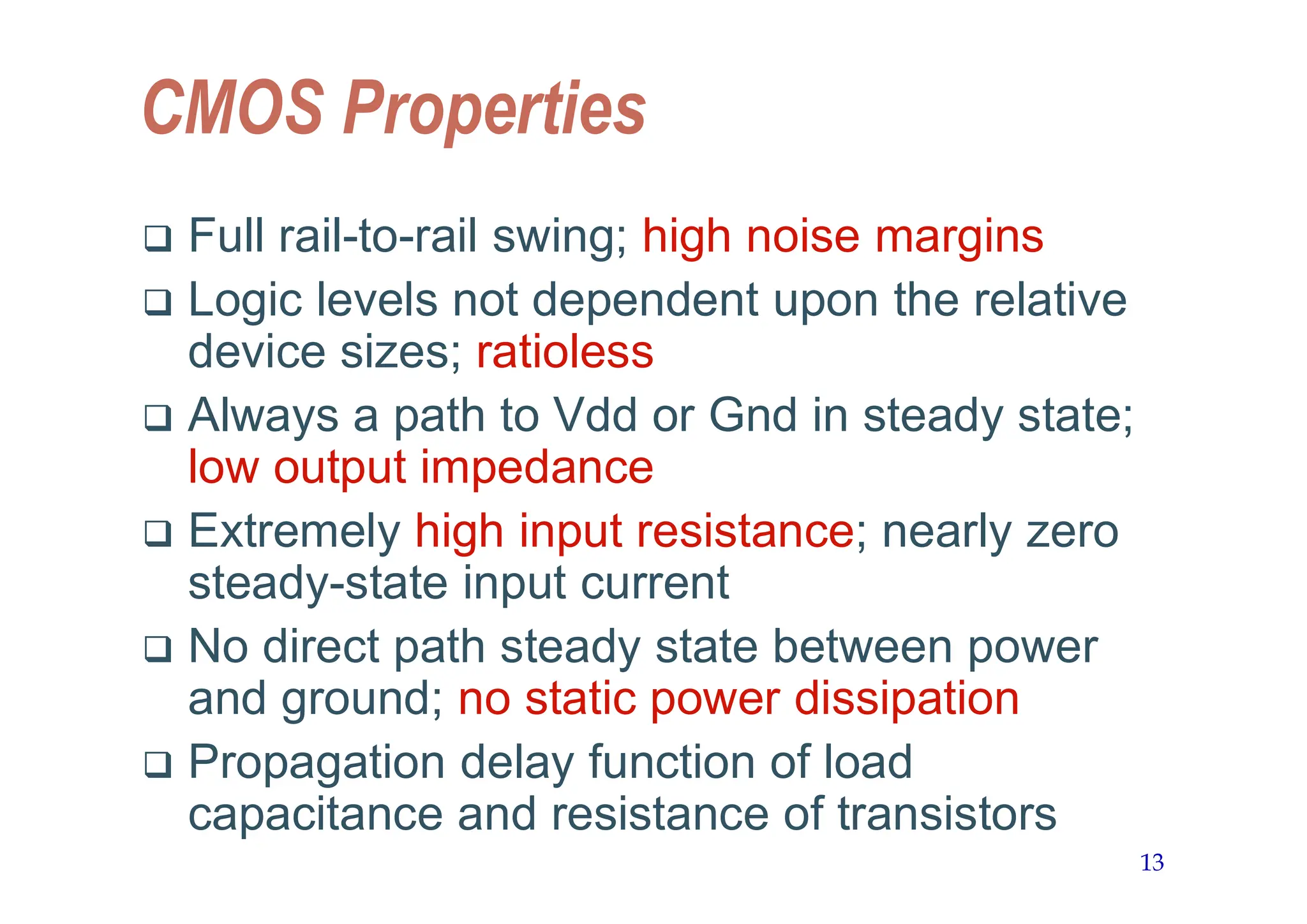
CMOS Properties
Fullrail-to-rail swing; high noise margins
Logic levels not dependent upon the relative
device sizes; ratioless
Always a path to Vdd or Gnd in steady state;
low output impedance
Extremely high input resistance; nearly zero
steady-state input current
No direct path steady state between power
and ground; no static power dissipation
Propagation delay function of load
capacitance and resistance of transistors
18
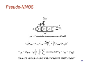
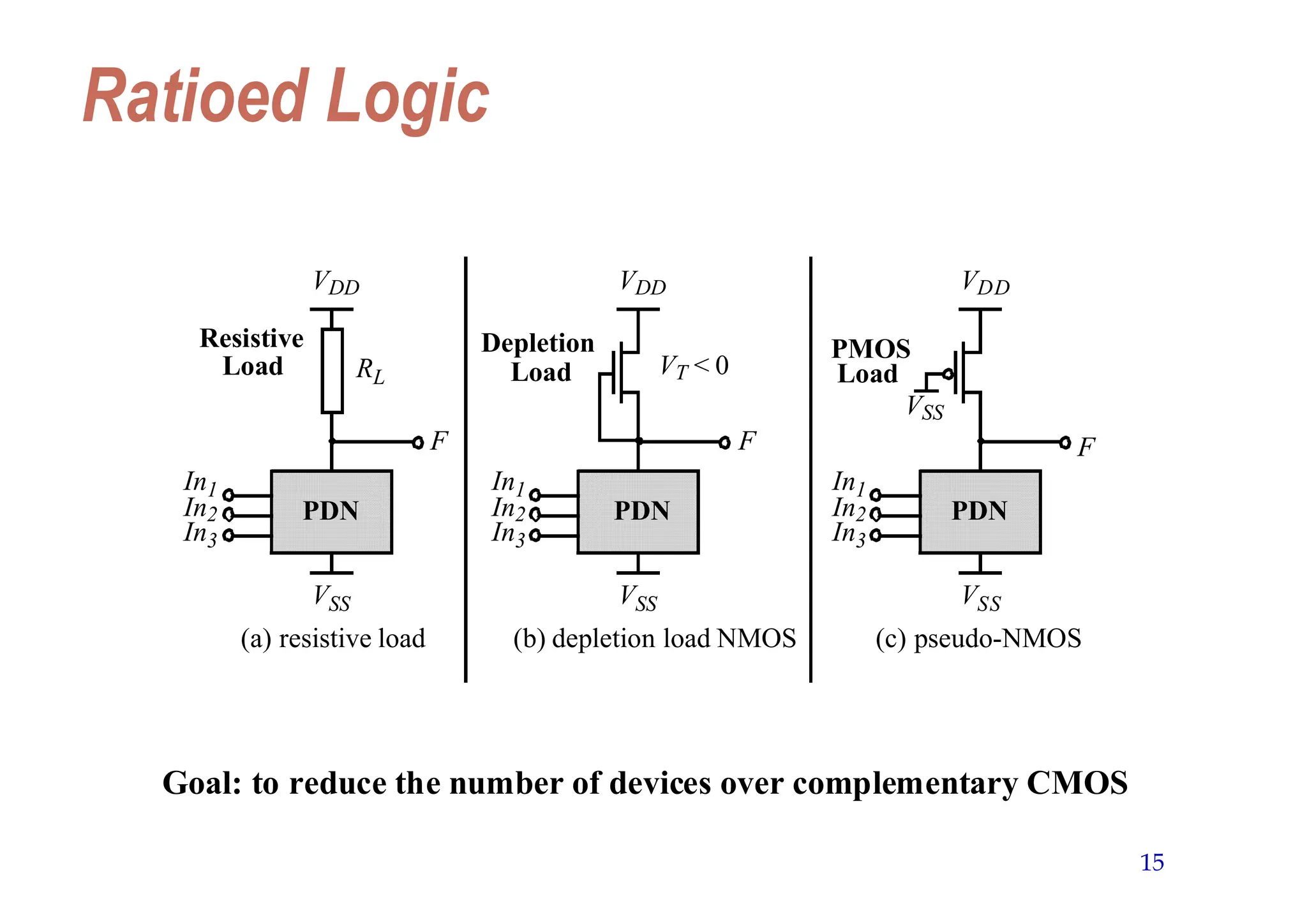
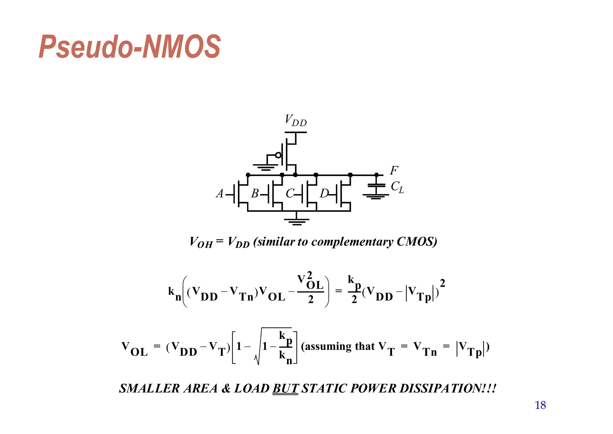
Pseudo-NMOS
VDD
A B CD
F
CL
VOH = VDD (similar to complementary CMOS)
k
n
V
DD
V
Tn
–
V
OL
V
OL
2
2
-------------
–
k
p
2
------ V
DD
V
Tp
–
2
=
V
OL
V
DD
V
T
–
1 1
kp
k
n
------
–
– (assuming that V
T
V
Tn
V
Tp
)
= = =
SMALLER AREA & LOAD BUT STATIC POWER DISSIPATION!!!