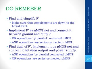
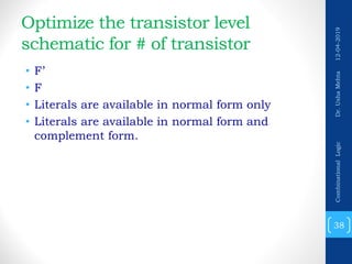
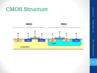
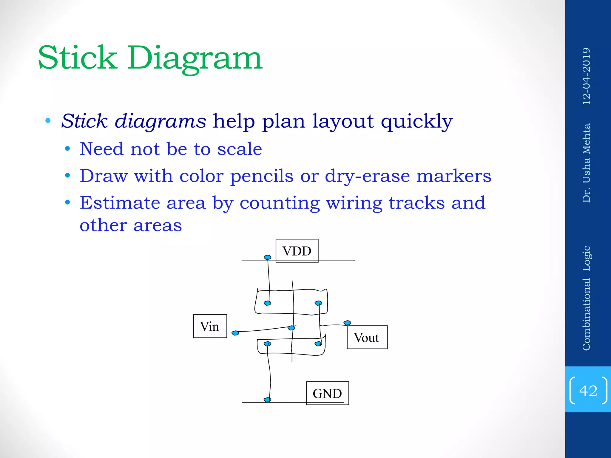
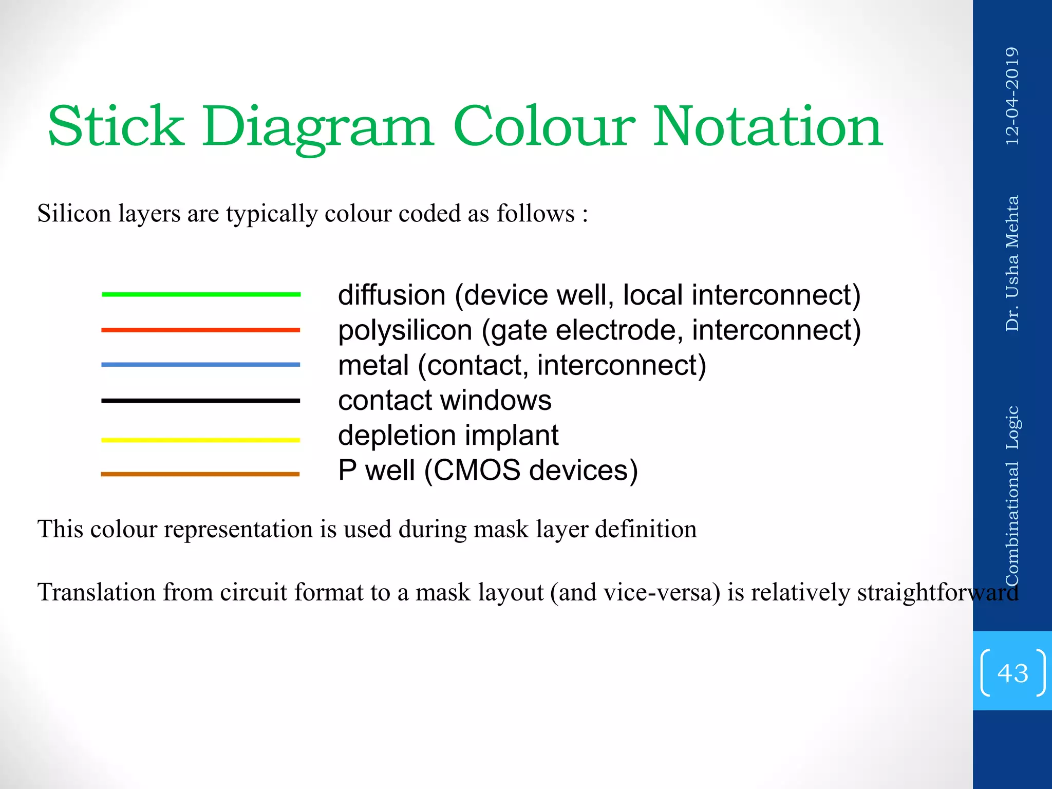
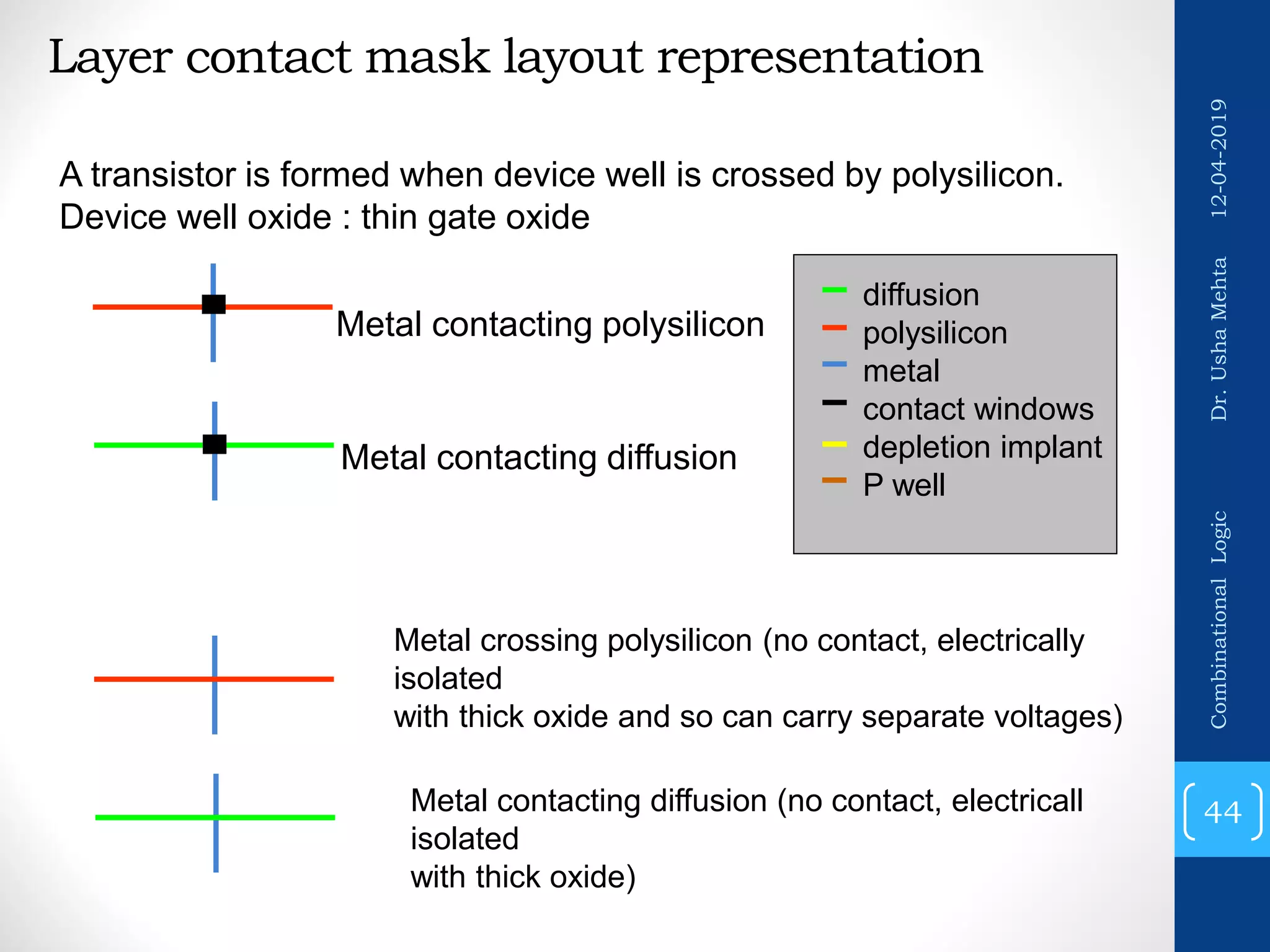
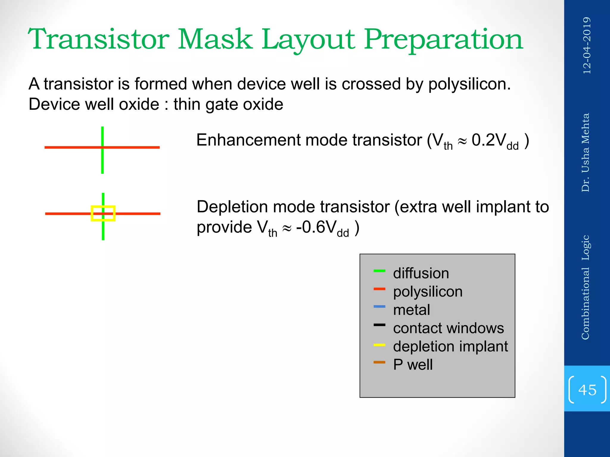
Download as PDF, PPTX


![Pull Up / Pull Down…..
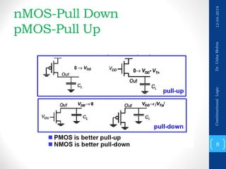
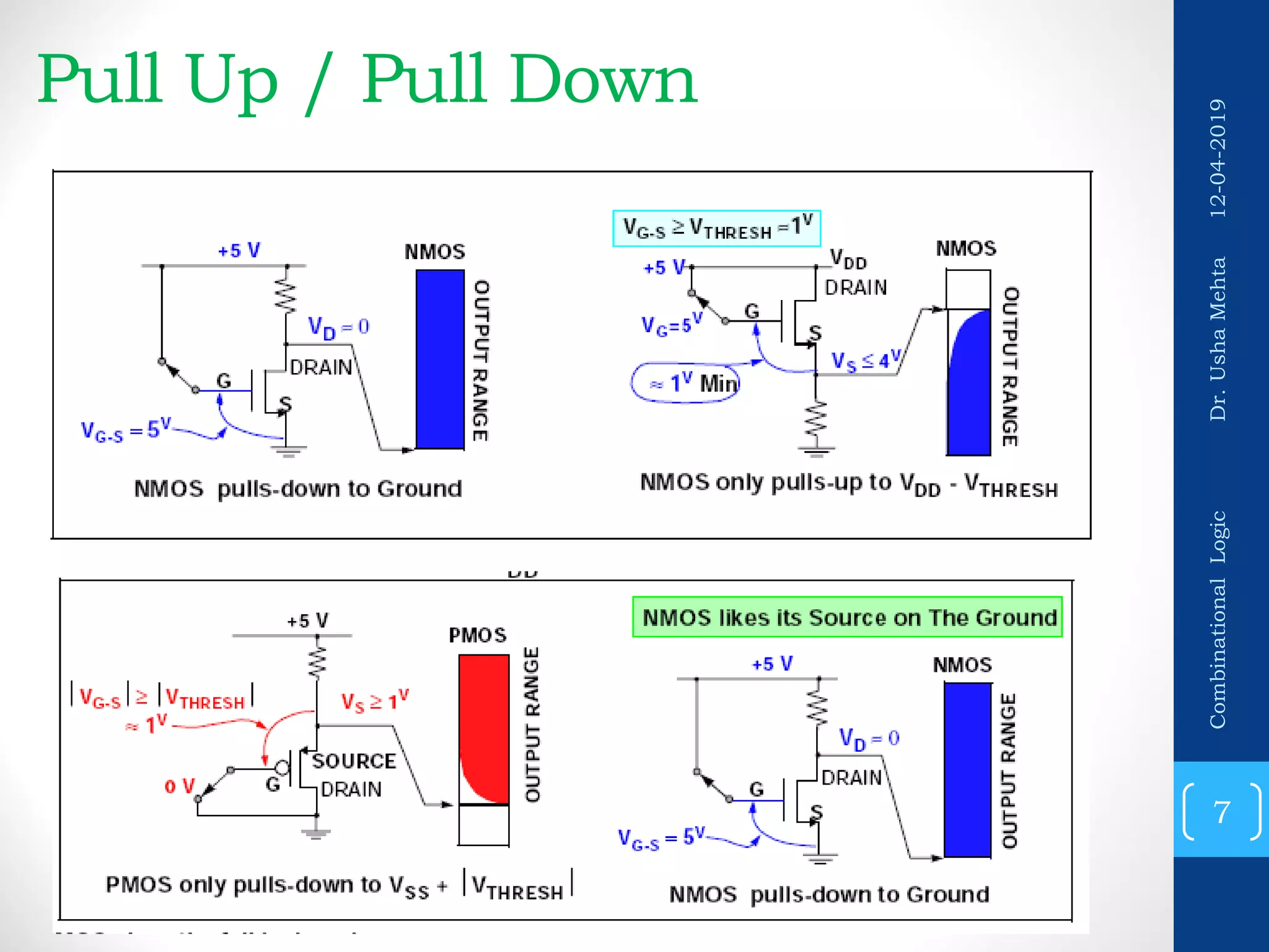
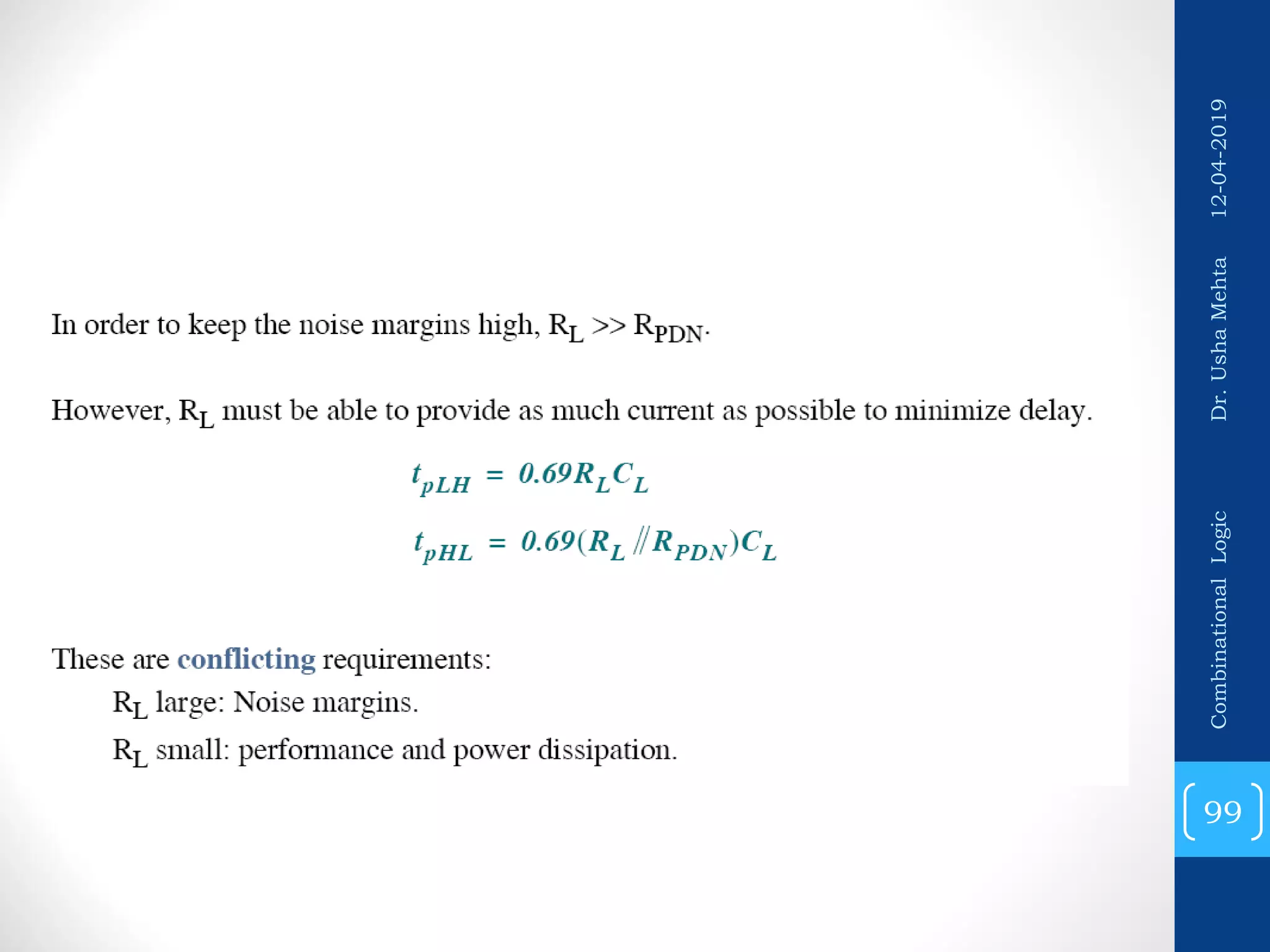
• For nMOS
• Vgs >= Vt
• 5-Vs>=1
• Vs = [0,4) i.e. ( 0 to Vg-Vt only, never Vg full is
coming to Vs)
• For pMOS
• Vgs =< Vt
• Vg-Vs =< Vt
• 0-Vs =< -1
• Vs = (1,5] i.e. ( 0 to Vg-Vt only, never Vg full is
coming to Vs)
12-04-2019CombinationalLogicDr.UshaMehta
9](https://image.slidesharecdn.com/6dvdcombinationaldesign-190826053512/85/Digital-VLSI-Design-Combinational-Circuit-9-320.jpg)


![Pull Up / Pull Down…..
• For nMOS
• Vgs >= Vt
• 5-Vs>=1
• Vs = [0,4) i.e. ( 0 to Vg-Vt only, never Vg full is
coming to Vs)
• For pMOS
• Vgs =< Vt
• Vg-Vs =< Vt
• 0-Vs =< -1
• Vs = (1,5] i.e. ( 0 to Vg-Vt only, never Vg full is
coming to Vs)
12-04-2019CombinationalLogicDr.UshaMehta
9](https://image.slidesharecdn.com/6dvdcombinationaldesign-190826053512/75/Digital-VLSI-Design-Combinational-Circuit-9-2048.jpg)
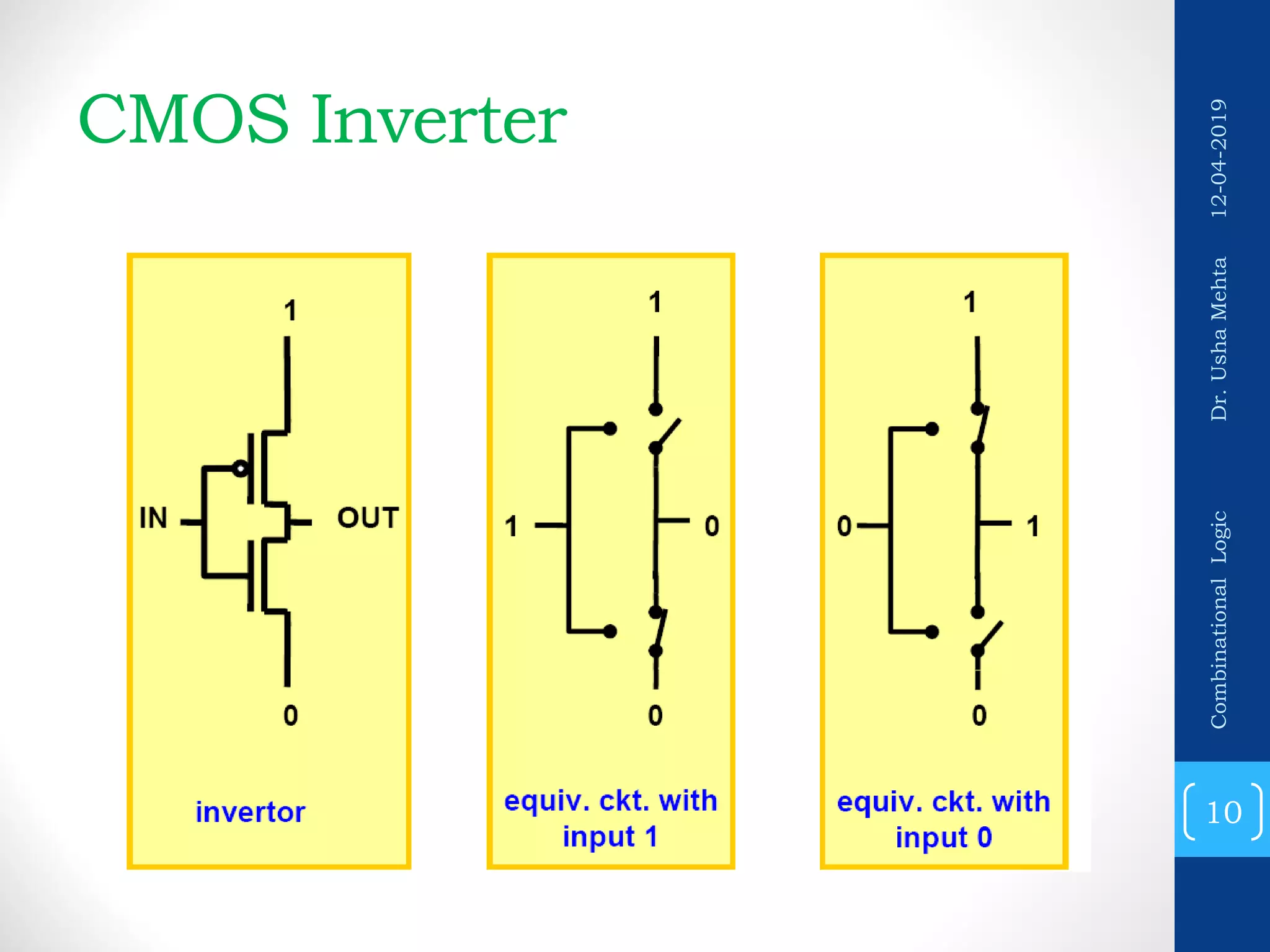
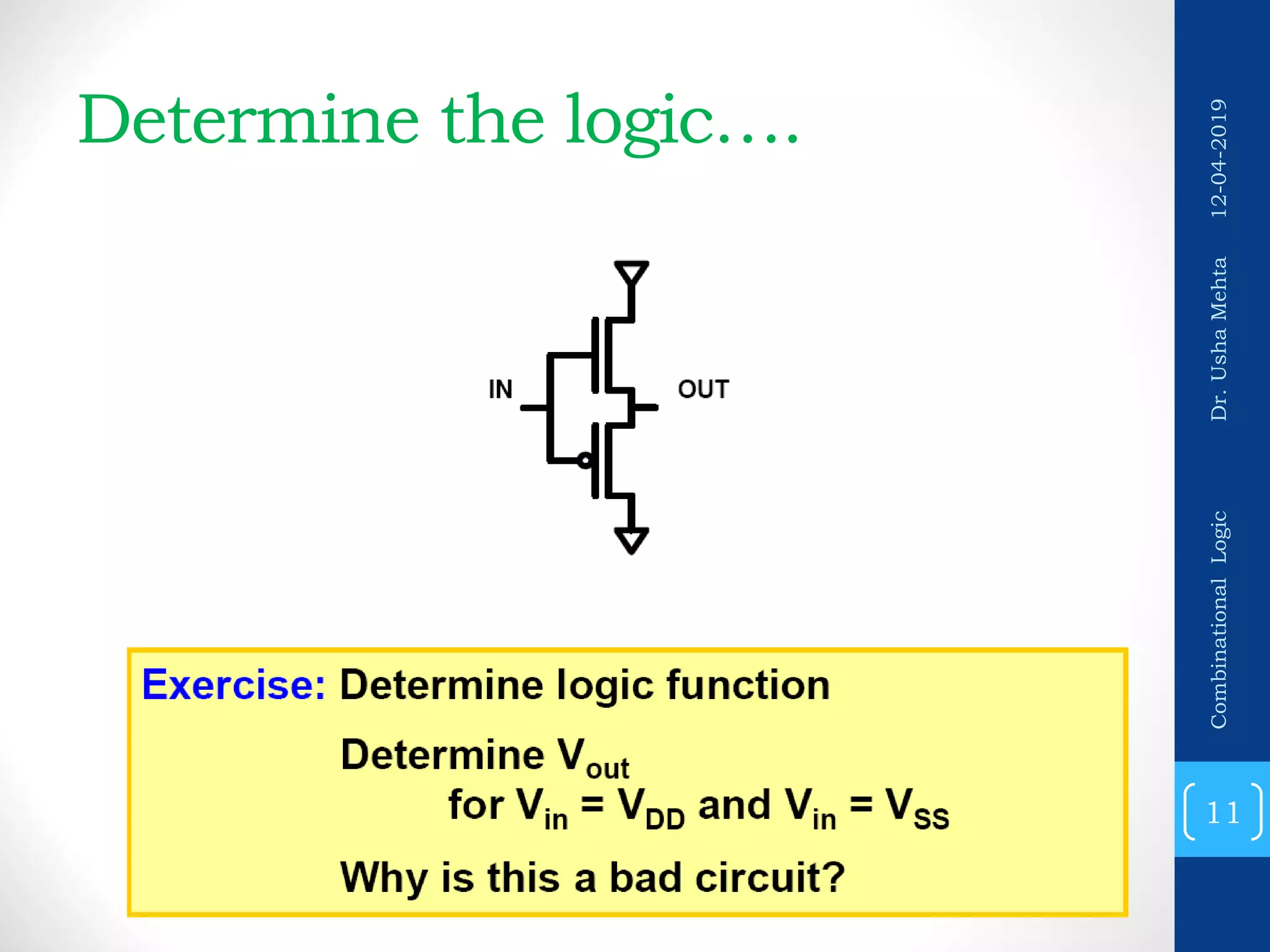
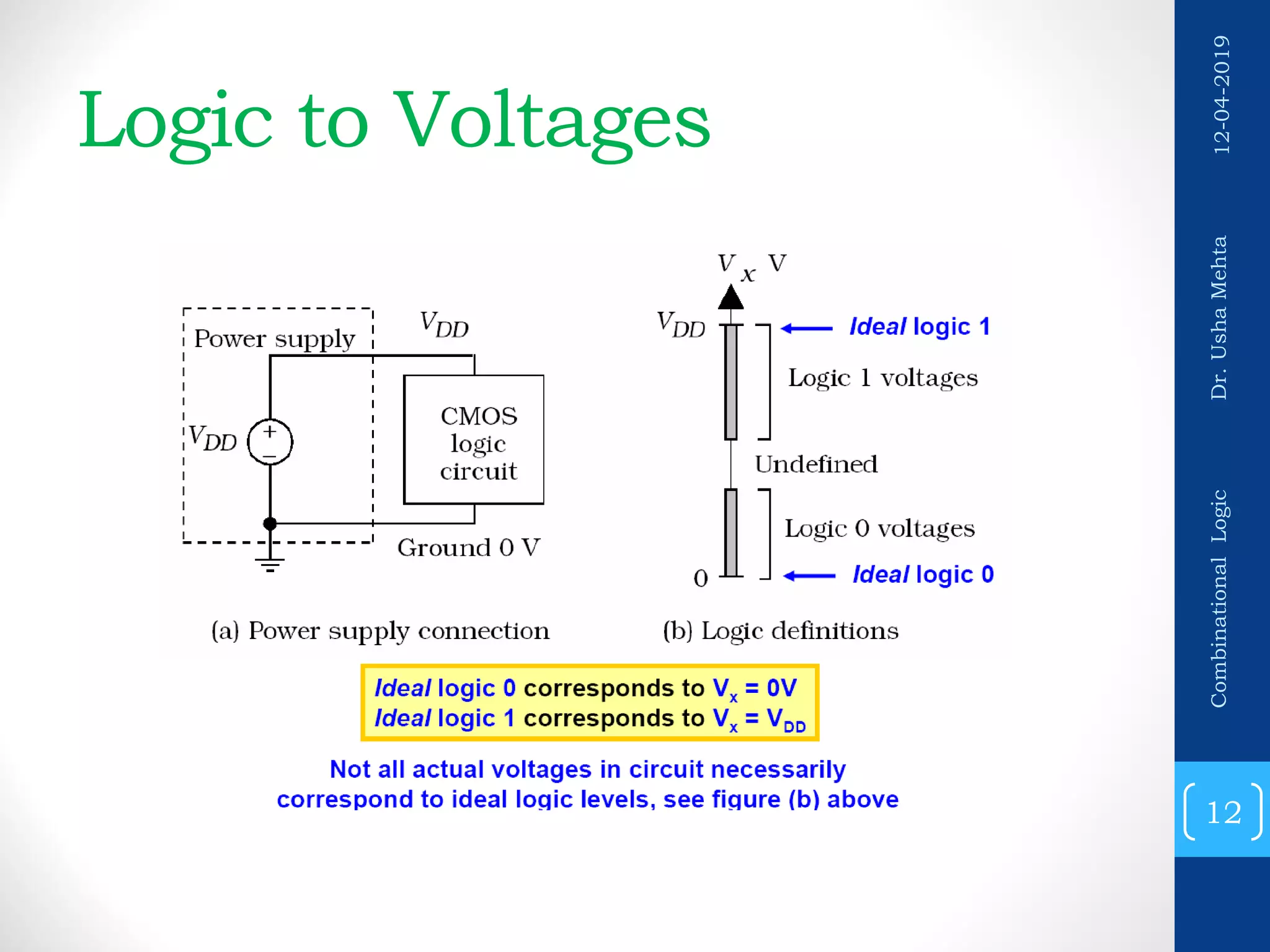
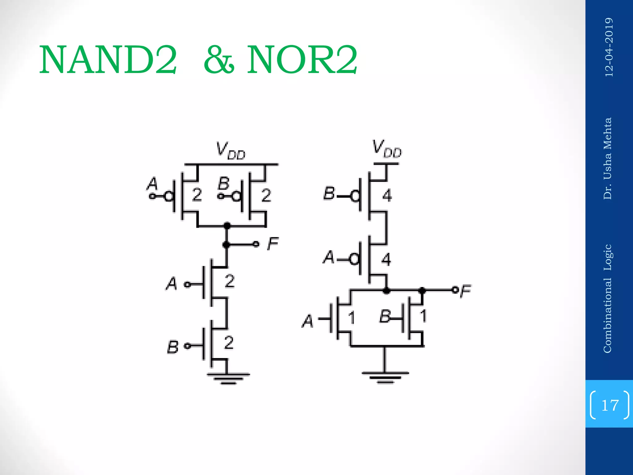
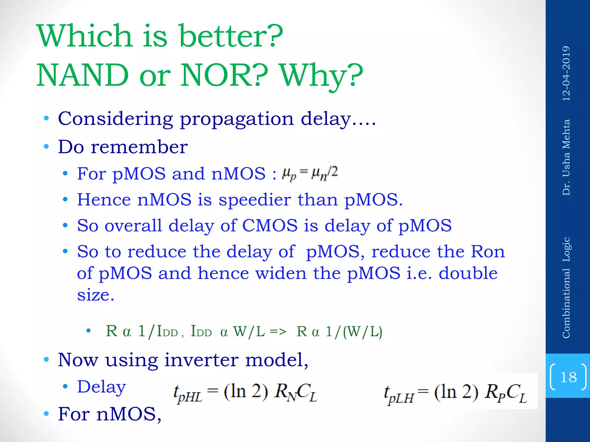
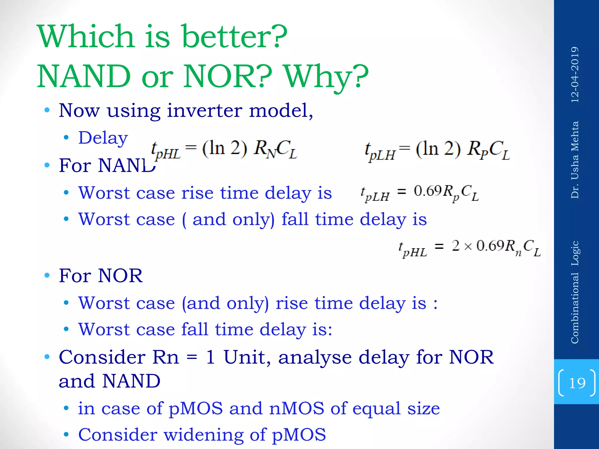


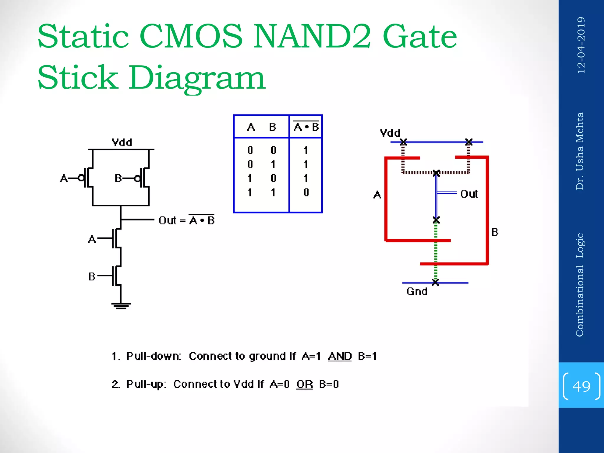
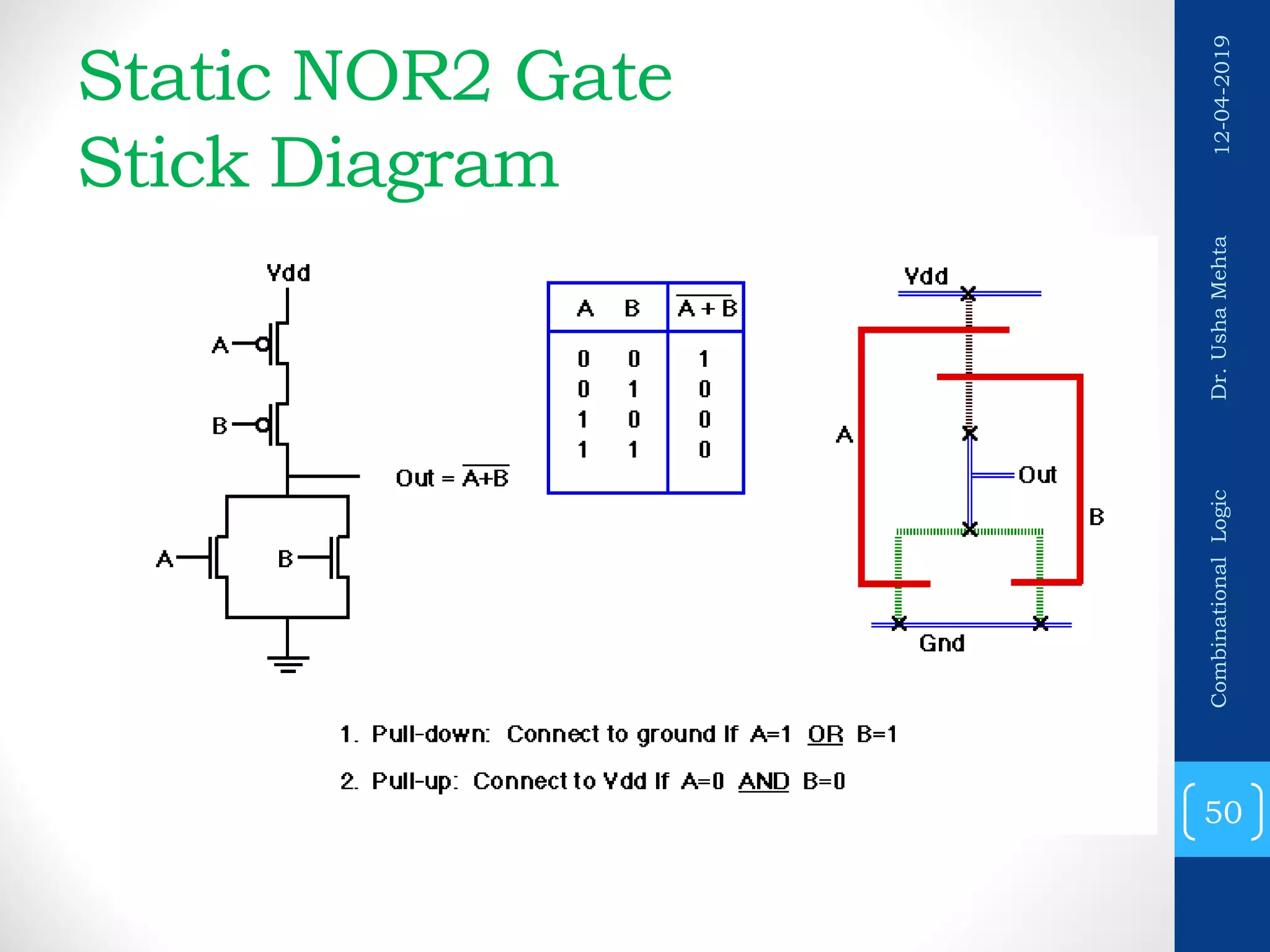
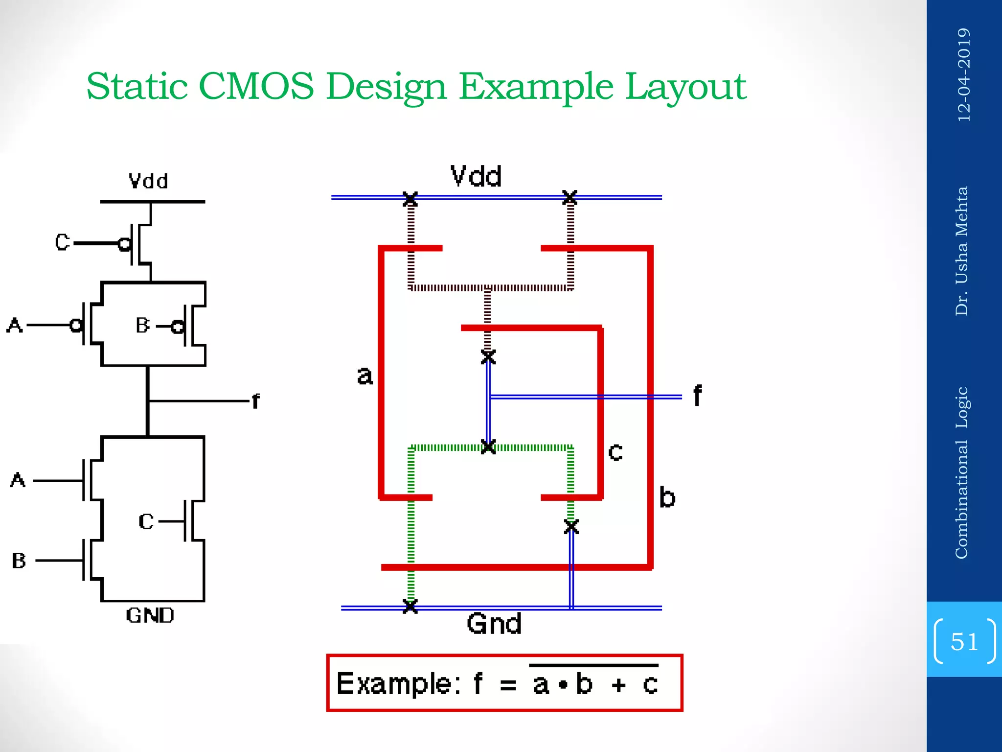
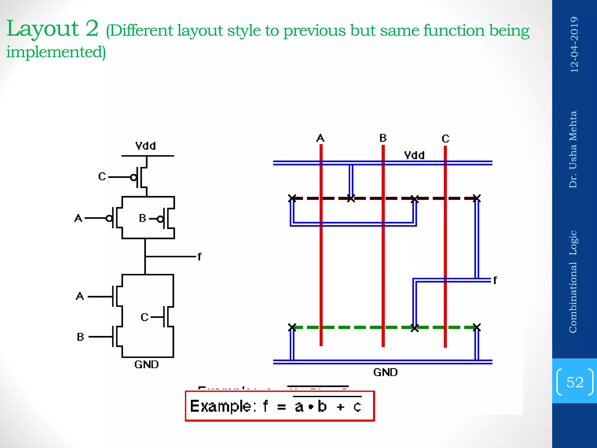
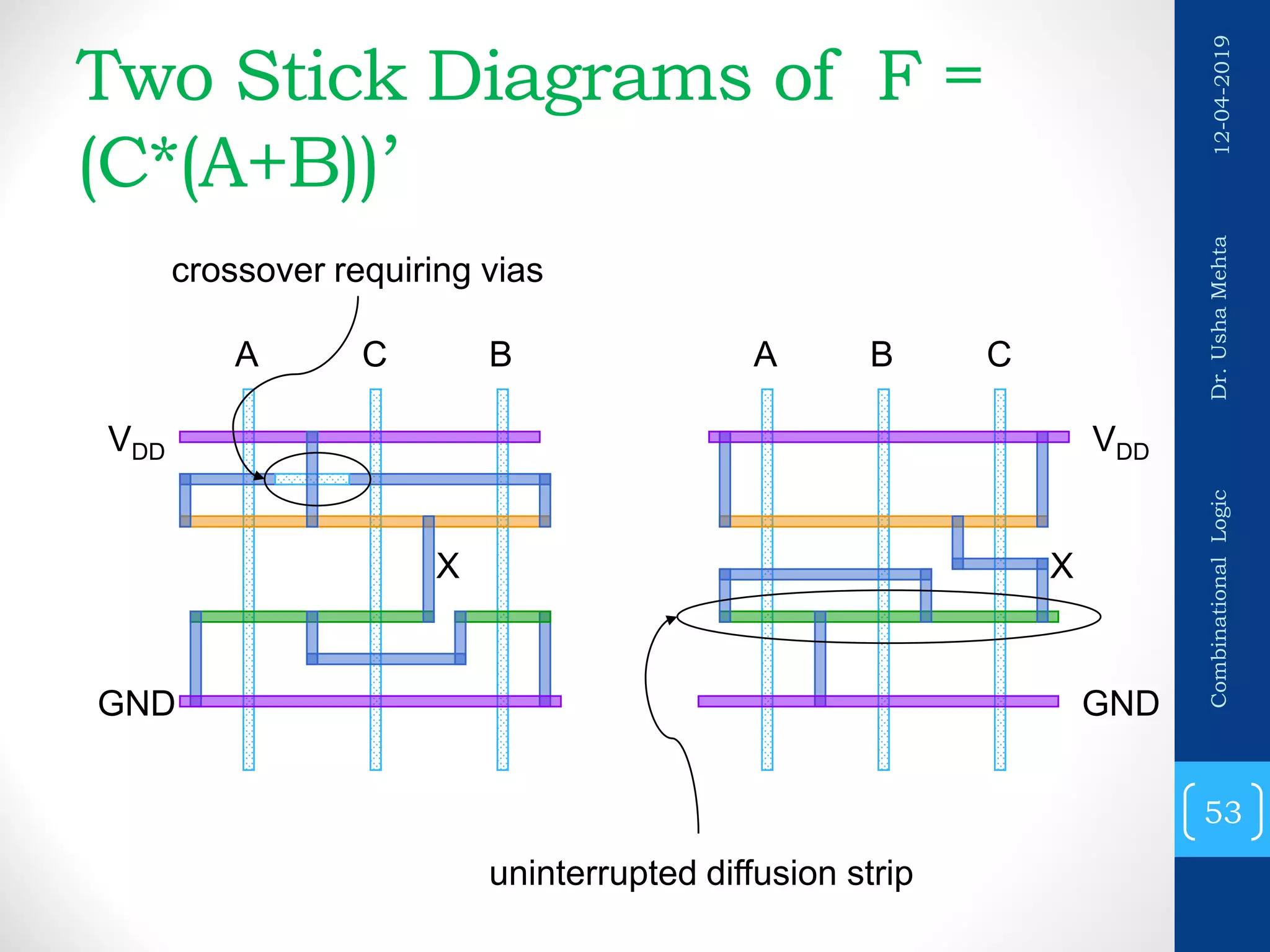

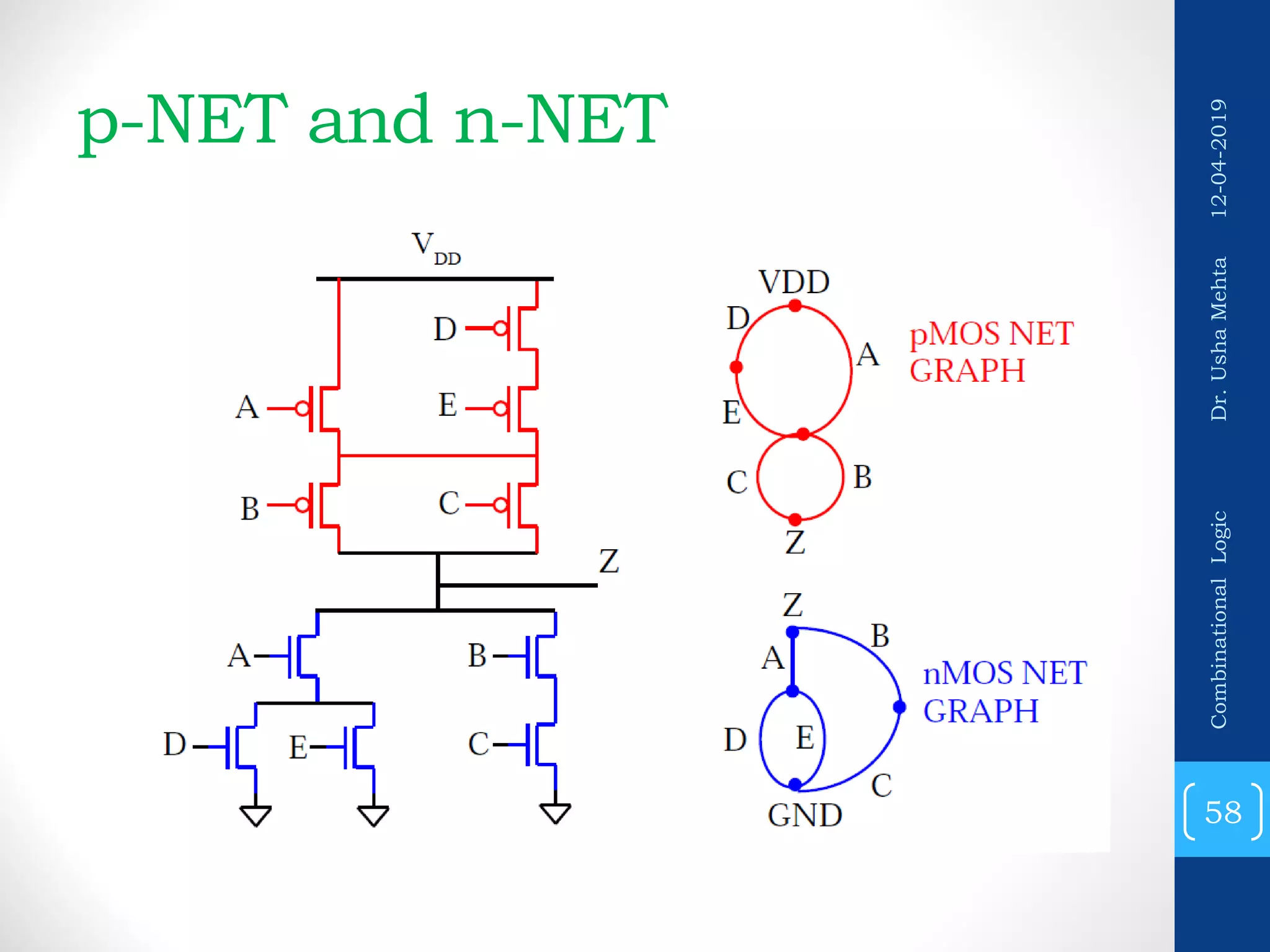
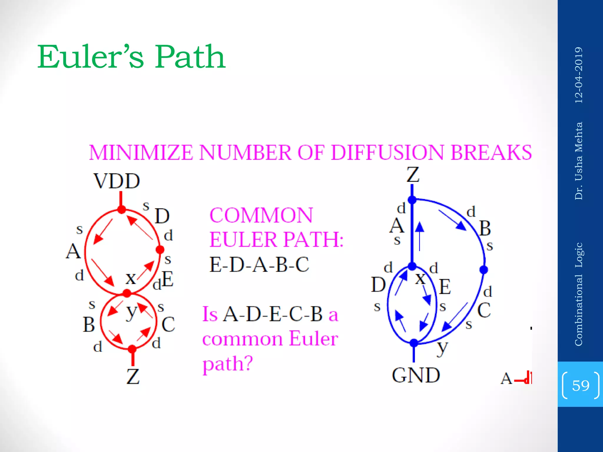
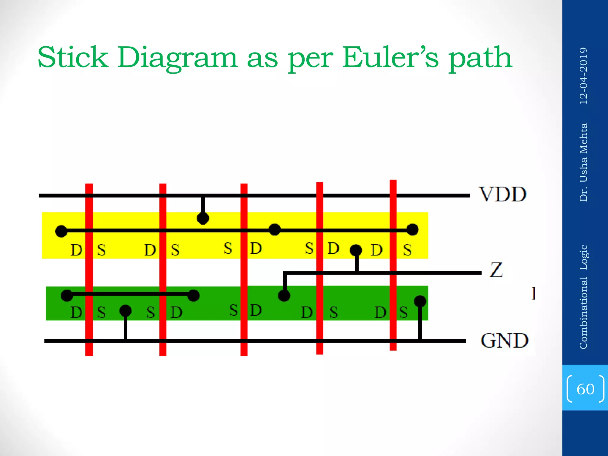
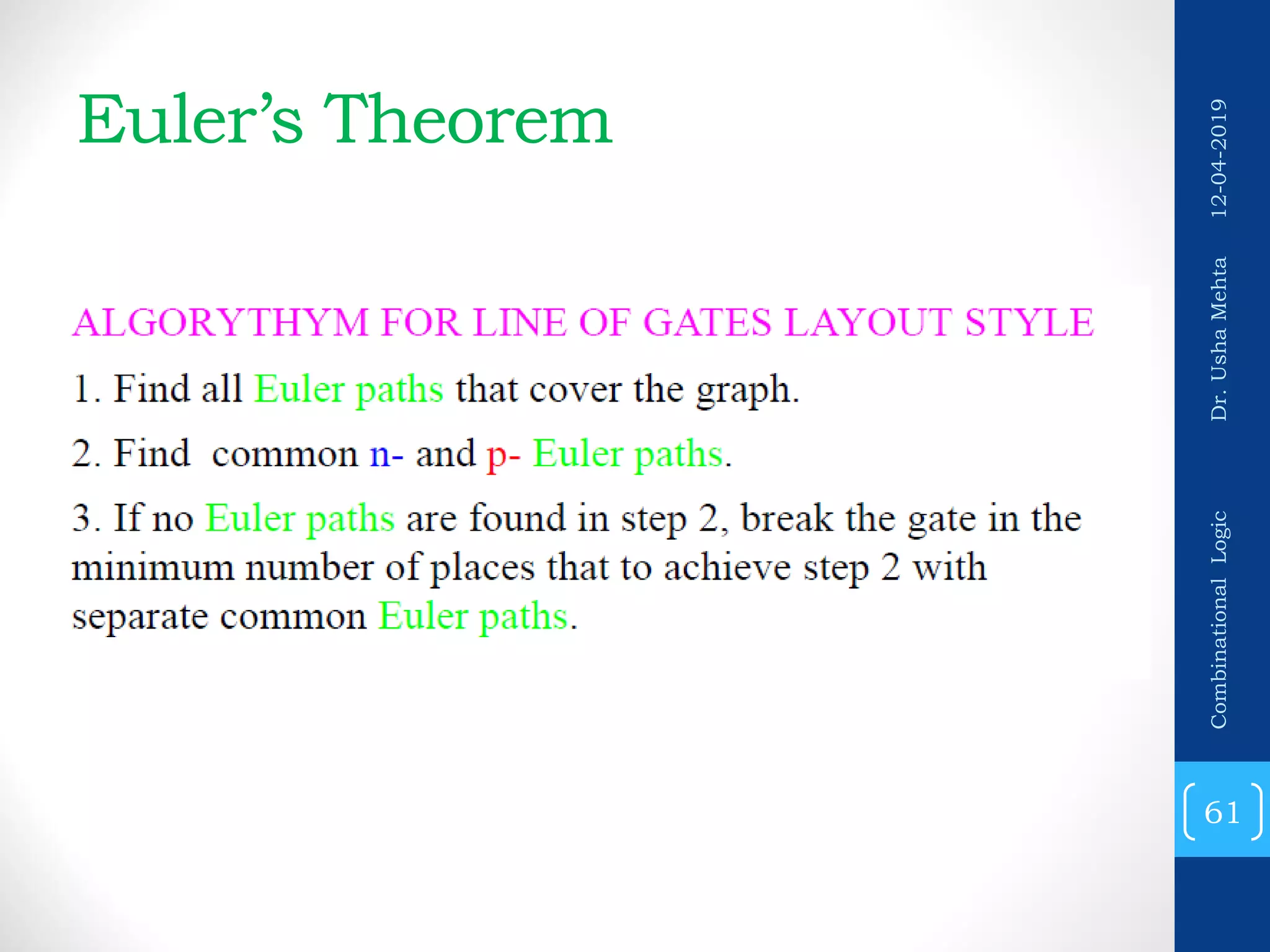
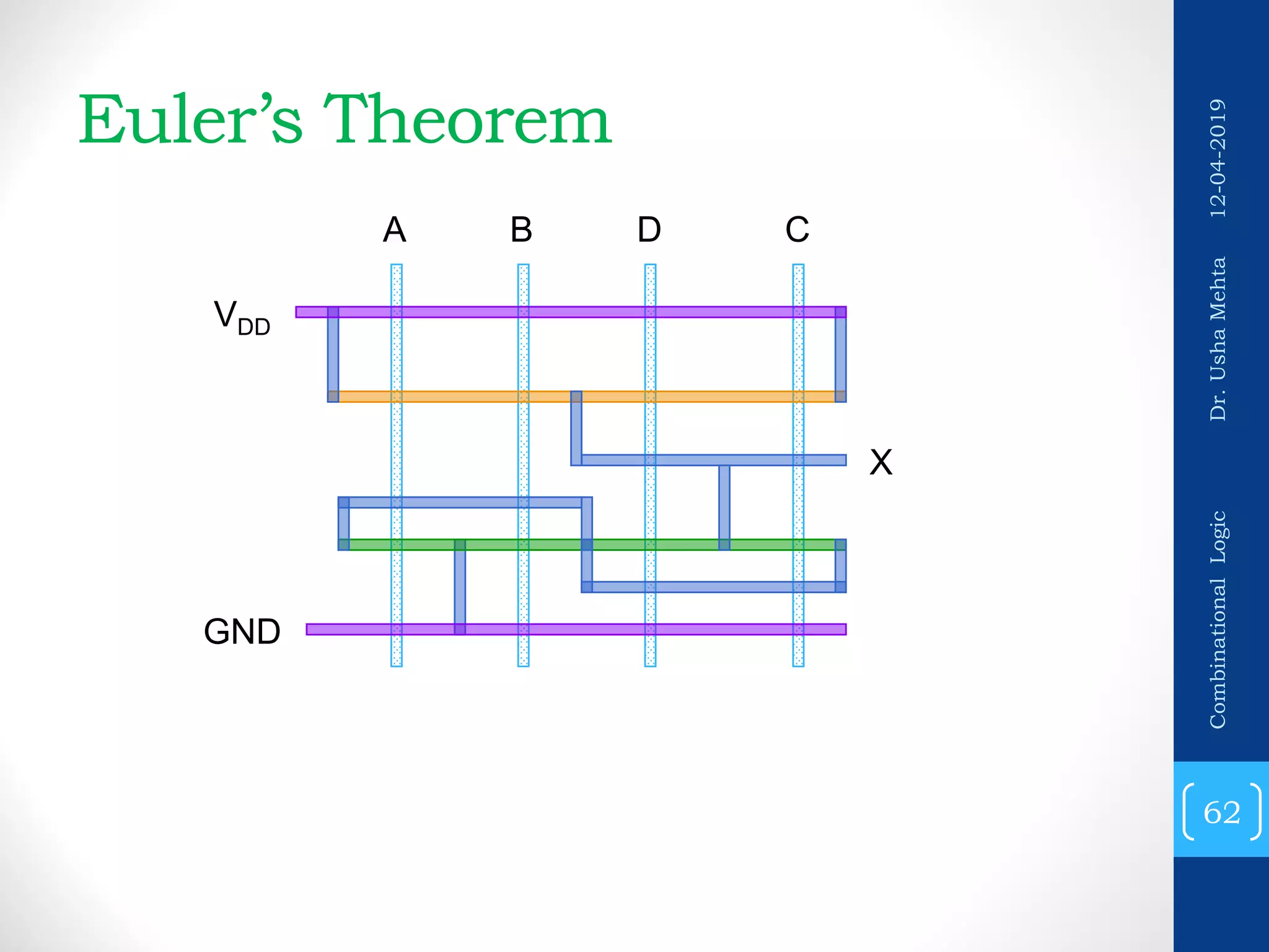


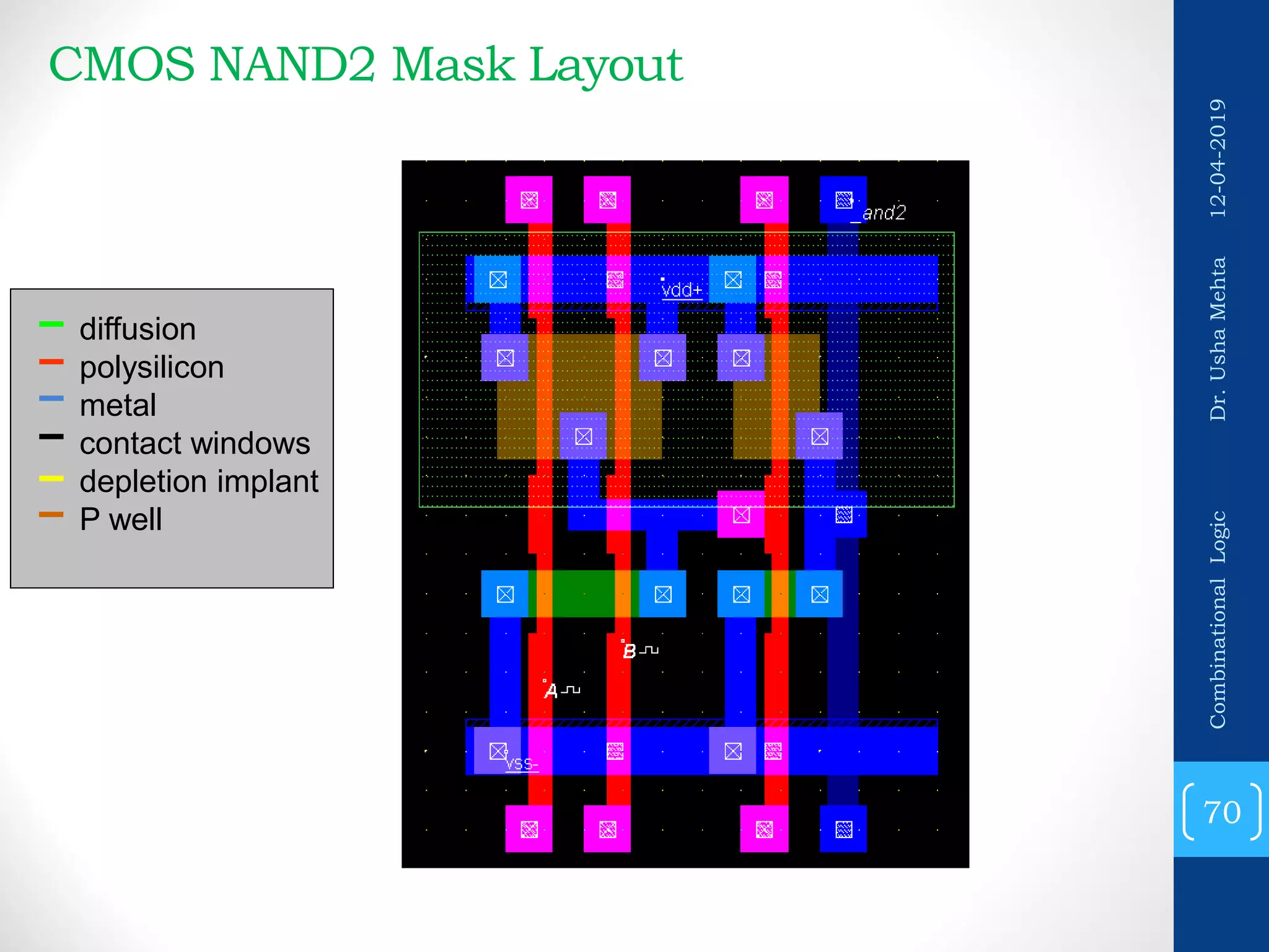
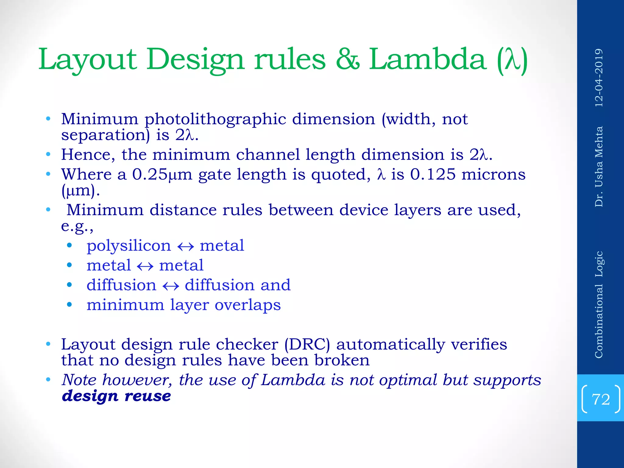
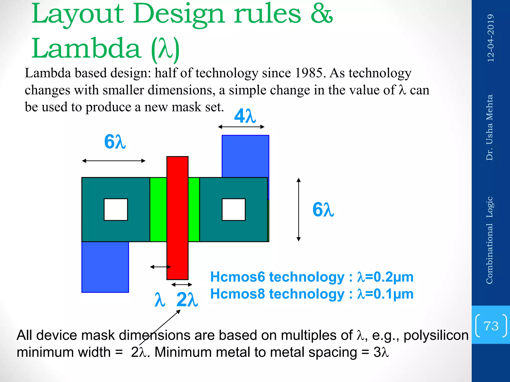
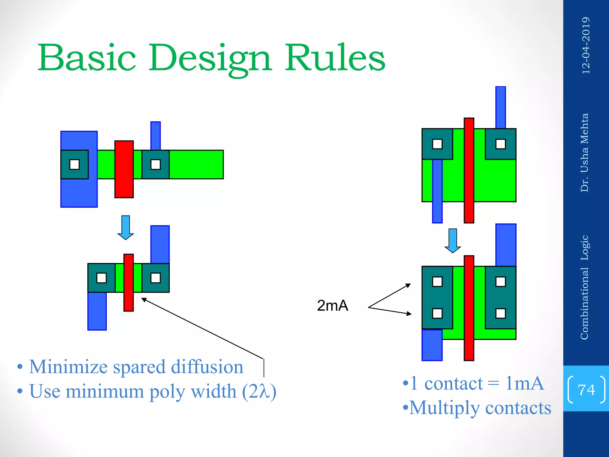
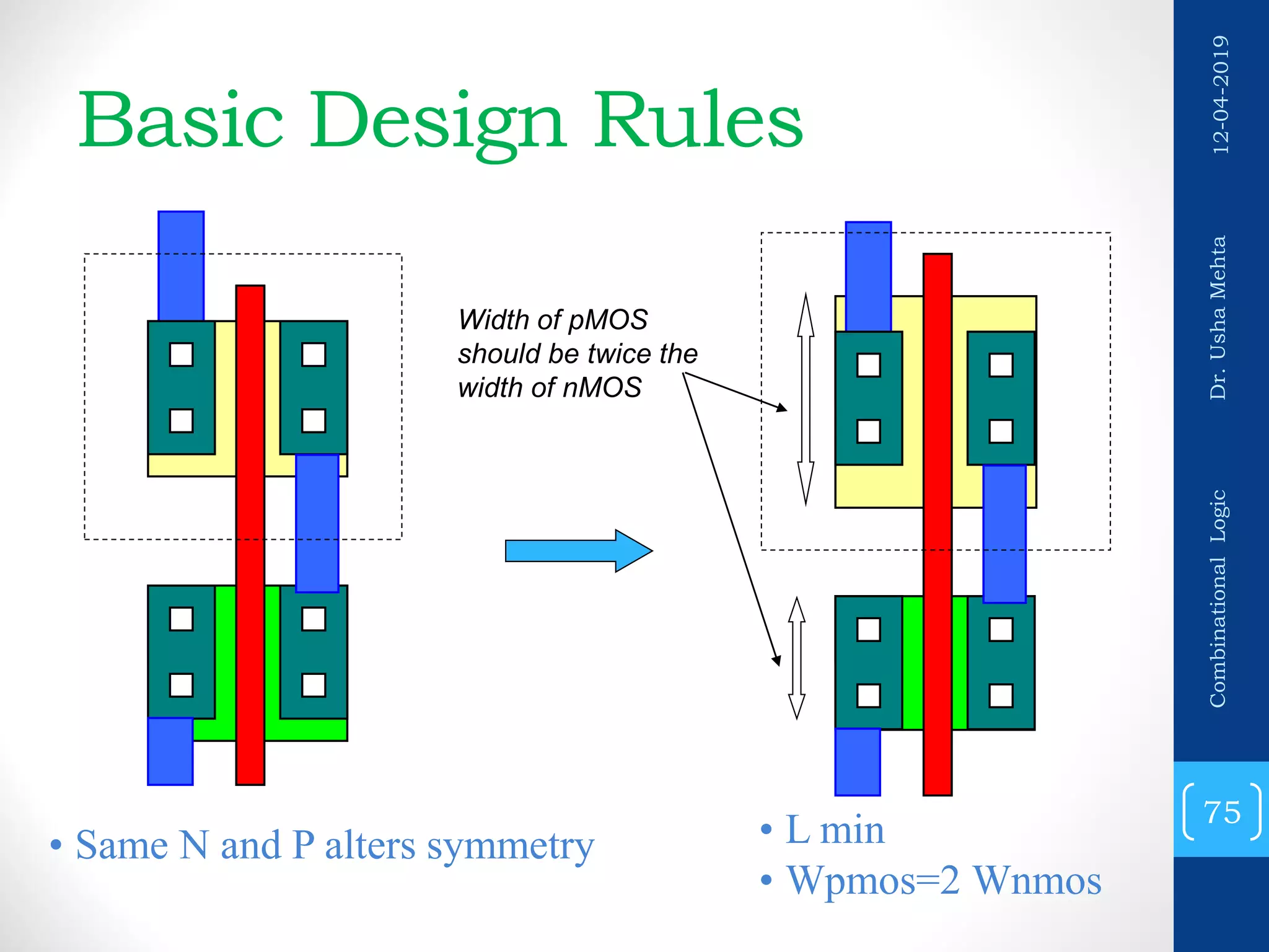


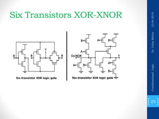
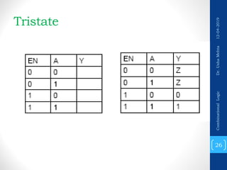
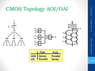
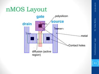
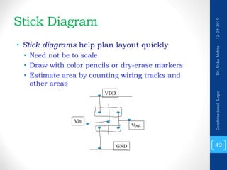
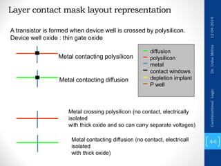
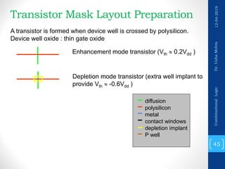
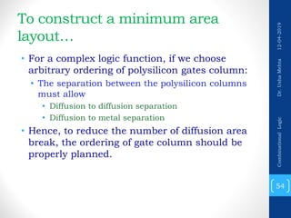
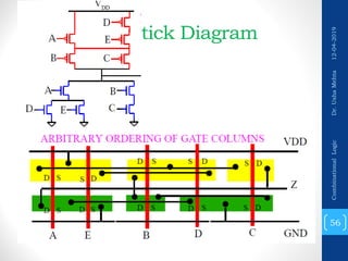
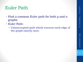
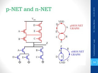
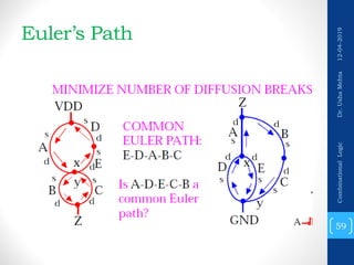
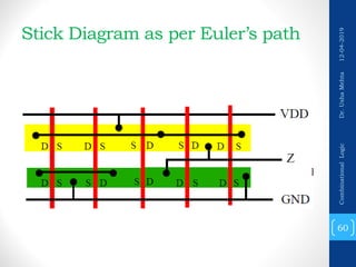
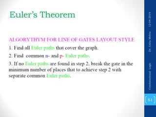
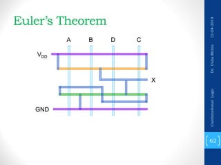
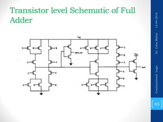
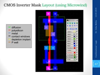
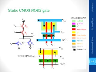
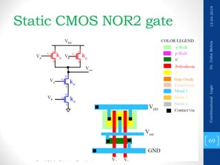
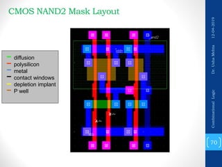
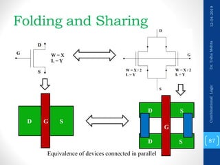
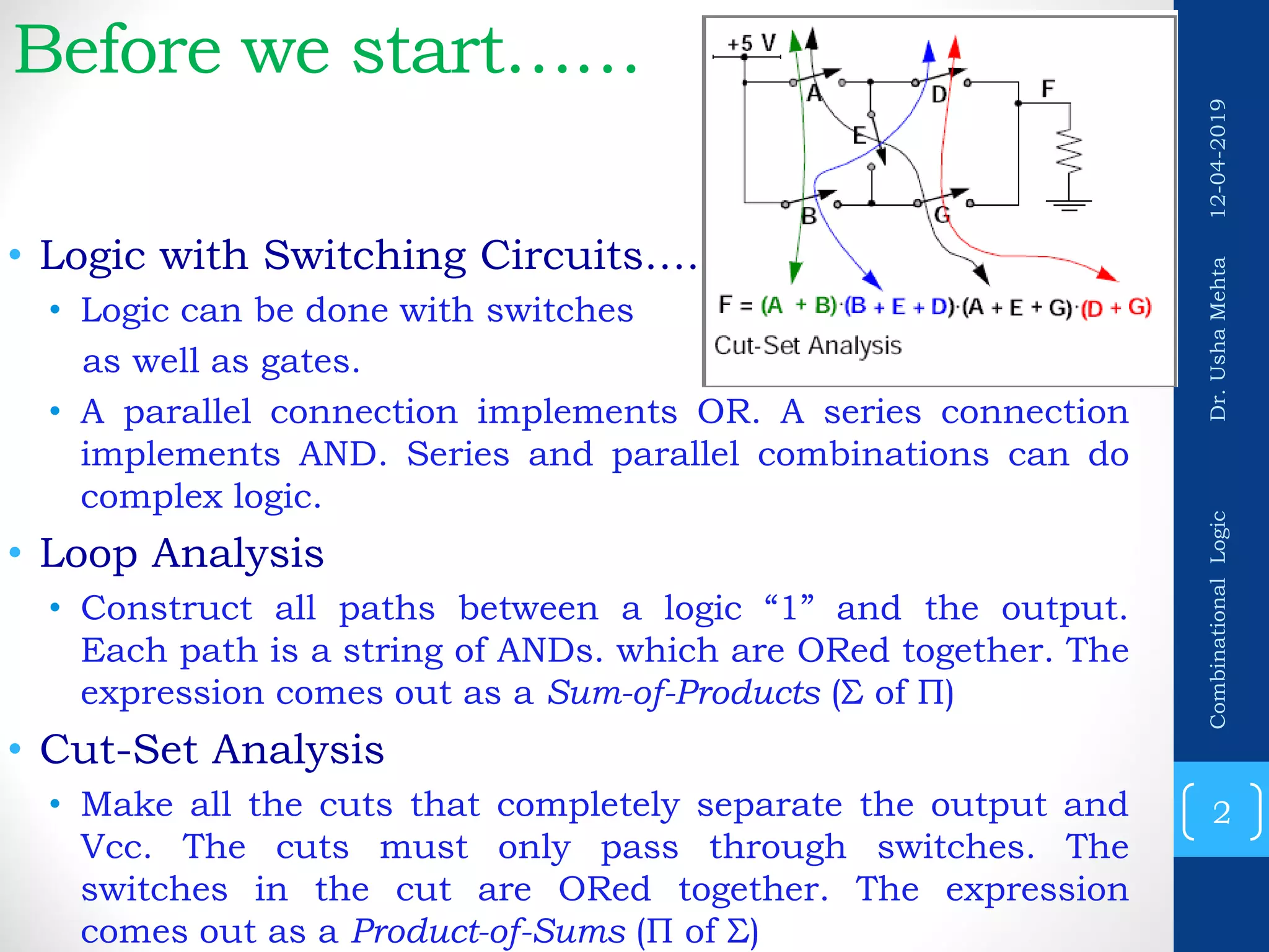
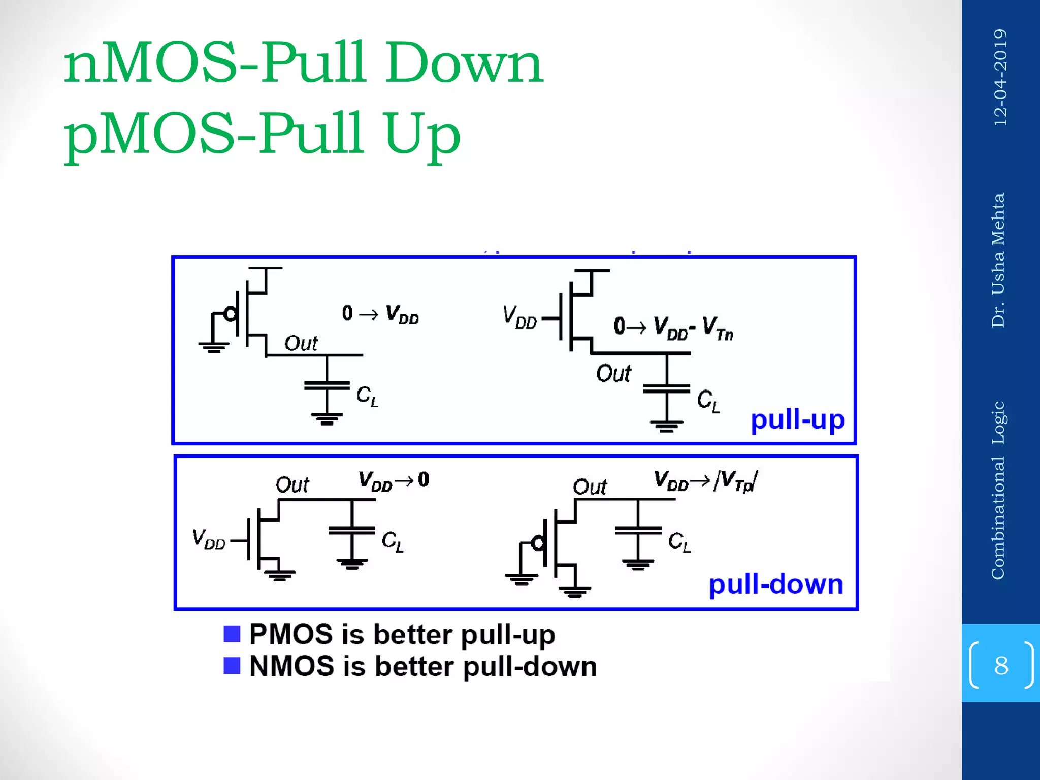
This document discusses combinational logic design and CMOS transistor implementation. It covers topics such as logic analysis techniques like loop and cut-set analysis, primitive logic gates, transistor-level implementations, and layout considerations. Primitive gates like NAND and NOR are shown along with complex functions. Optimization techniques for transistor count and layout area are presented, including Euler path analysis and ensuring a continuous diffusion path. Design rules for lambda-based layout and considerations for transistor sizing are also outlined.


