Lecture Notes - Microprocessor - Unit 2 - 8085 Pinout signal, Functional Block Diagram and Instruction Set
Description:
Welcome to the comprehensive guide on Microprocessor and micro controller tailored for First year (Second Semester) B.Sc. Computer Science students affiliated with Alagappa University. This document covers fundamental concepts of microprocessor and micro controller. PDF content is prepared from the text book R. S. Gaonkar- "Microprocessor Architecture- Programming and Applications with 8085"- 5th Edition
Key Topics Covered:
Main Topic : Pinout signal, Functional Block Diagram and Instruction Set
Sub-Topic :
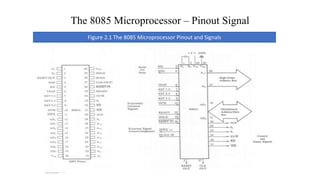
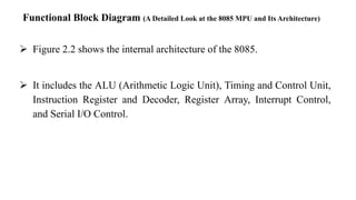
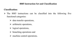
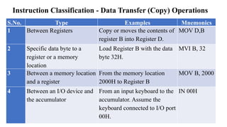
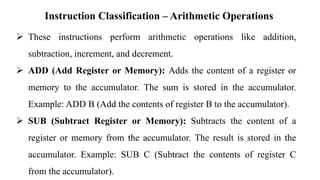
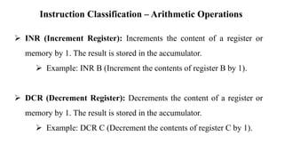
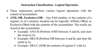
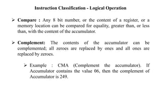
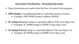
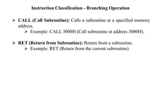
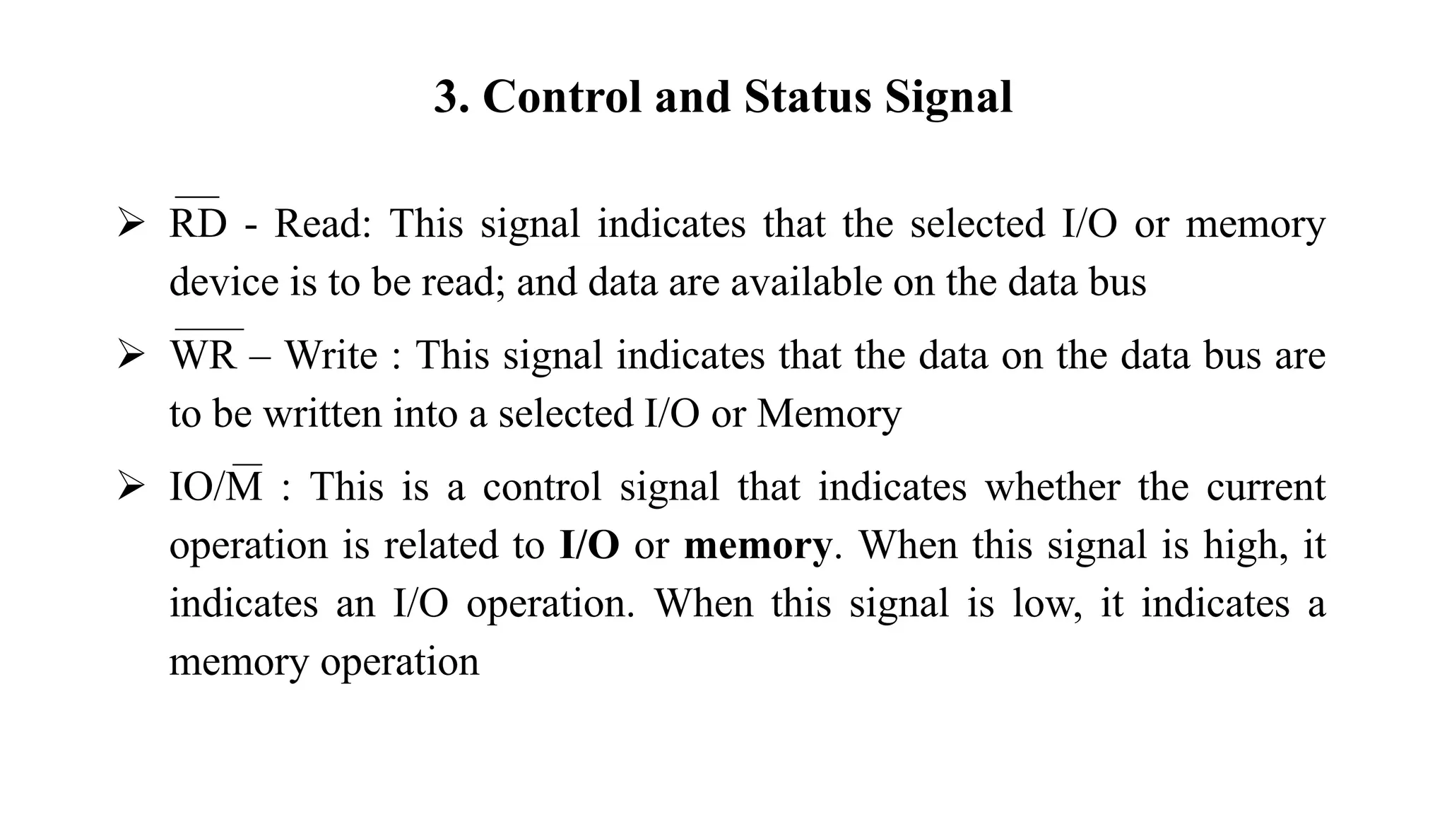
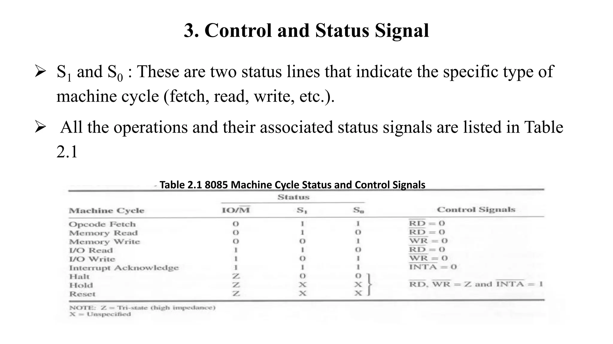
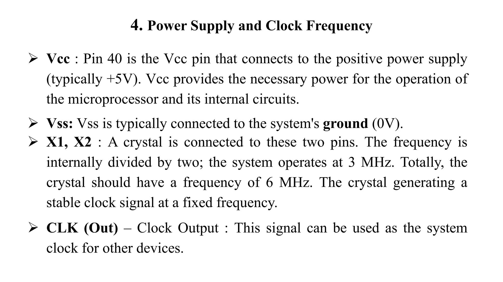
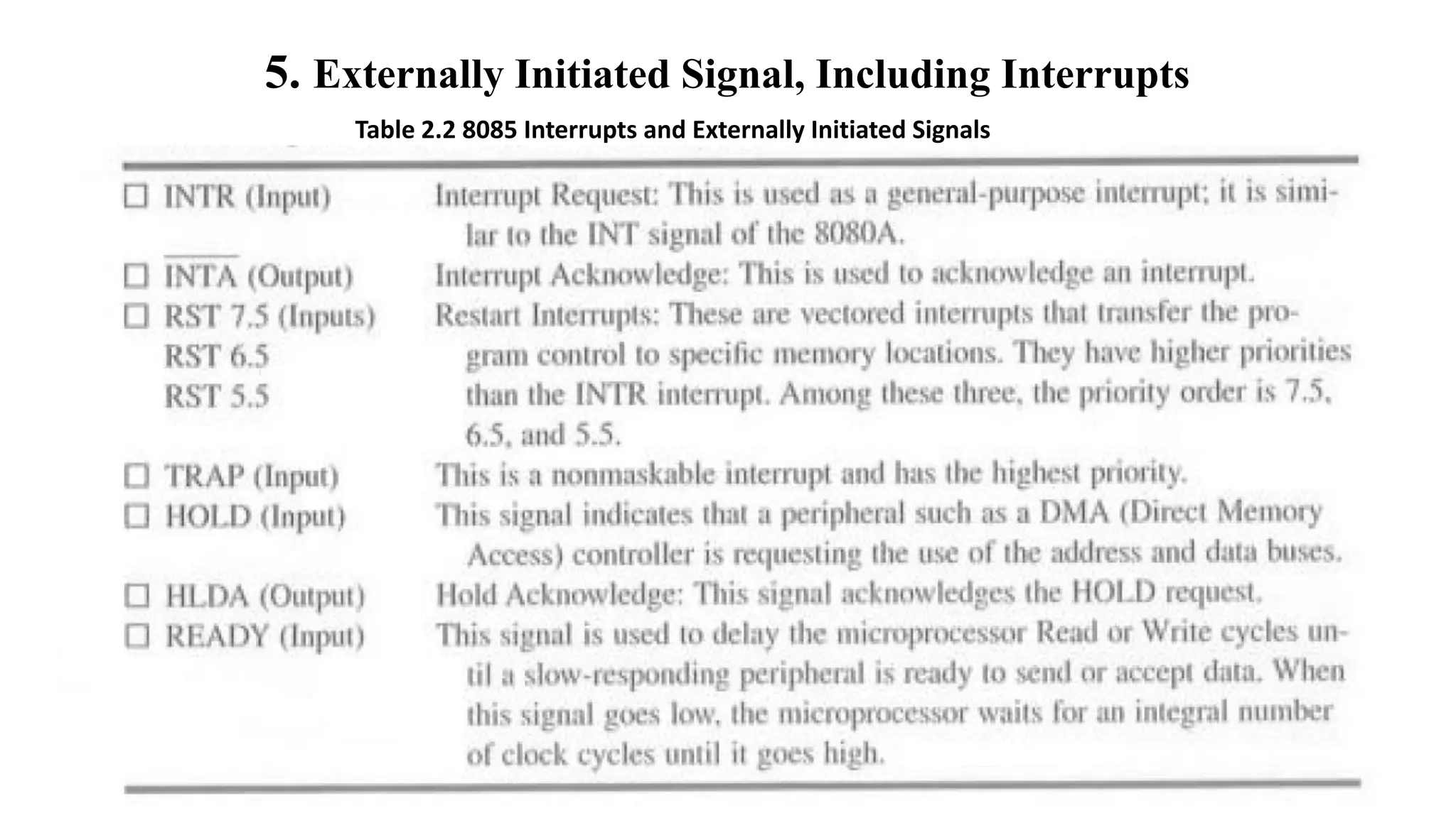
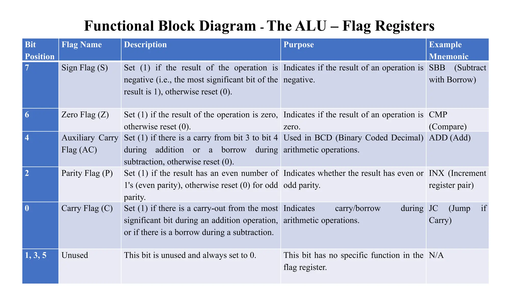
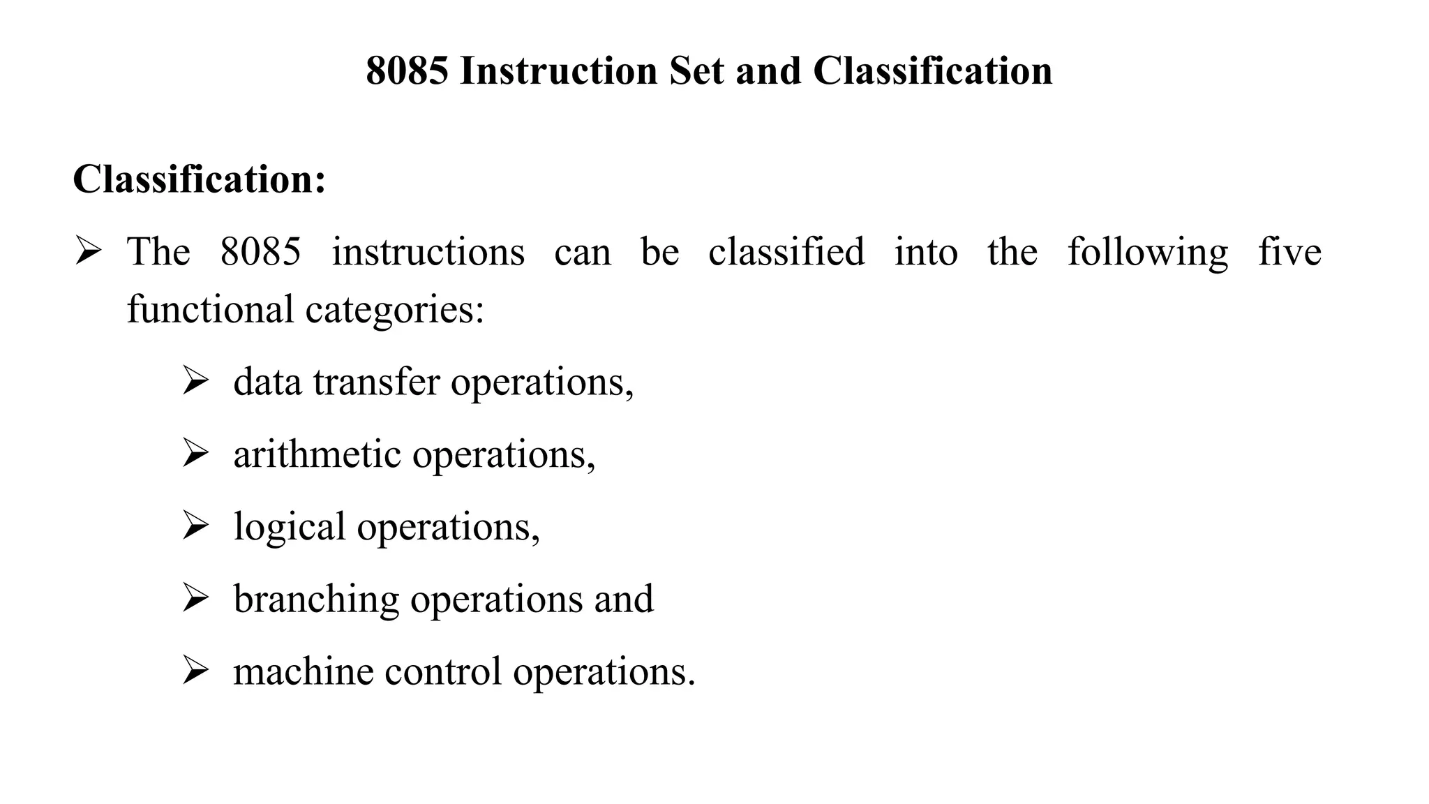
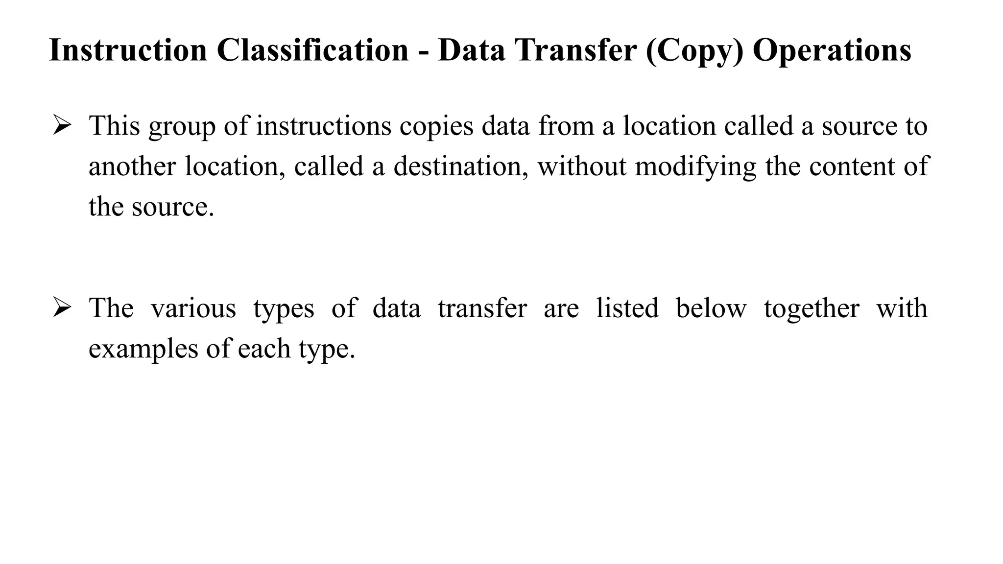
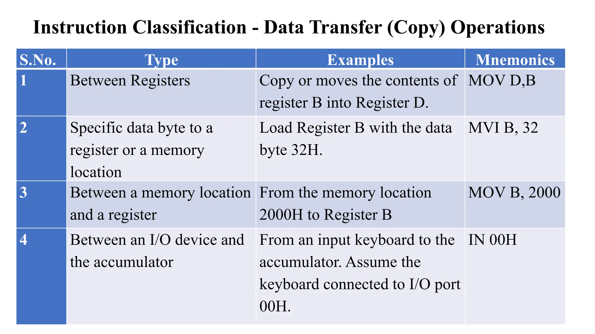
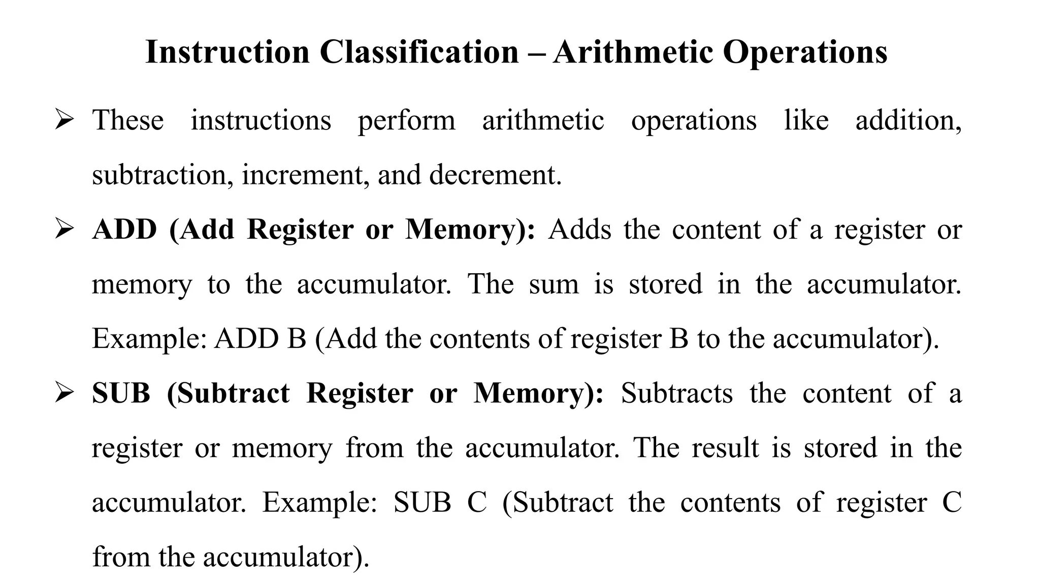
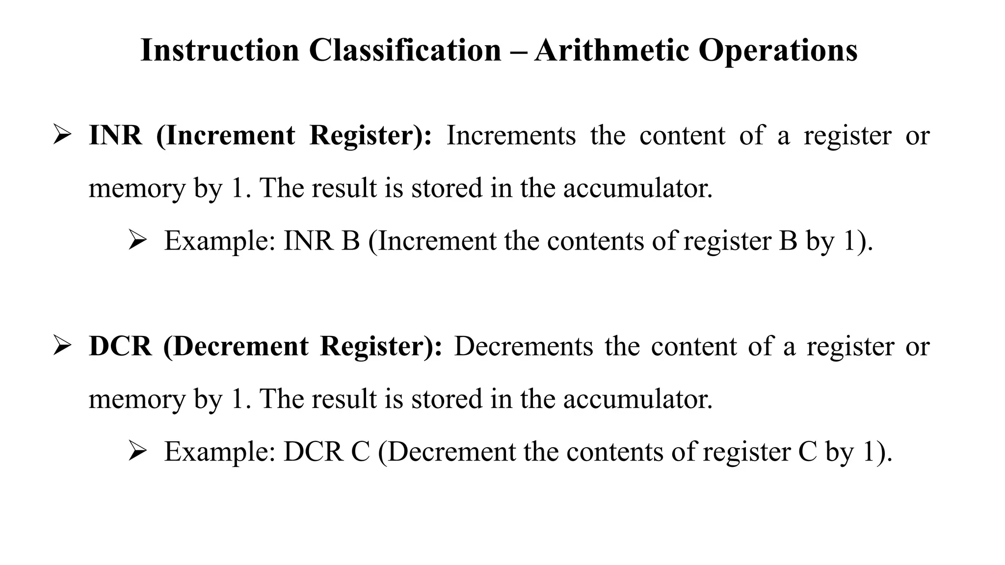
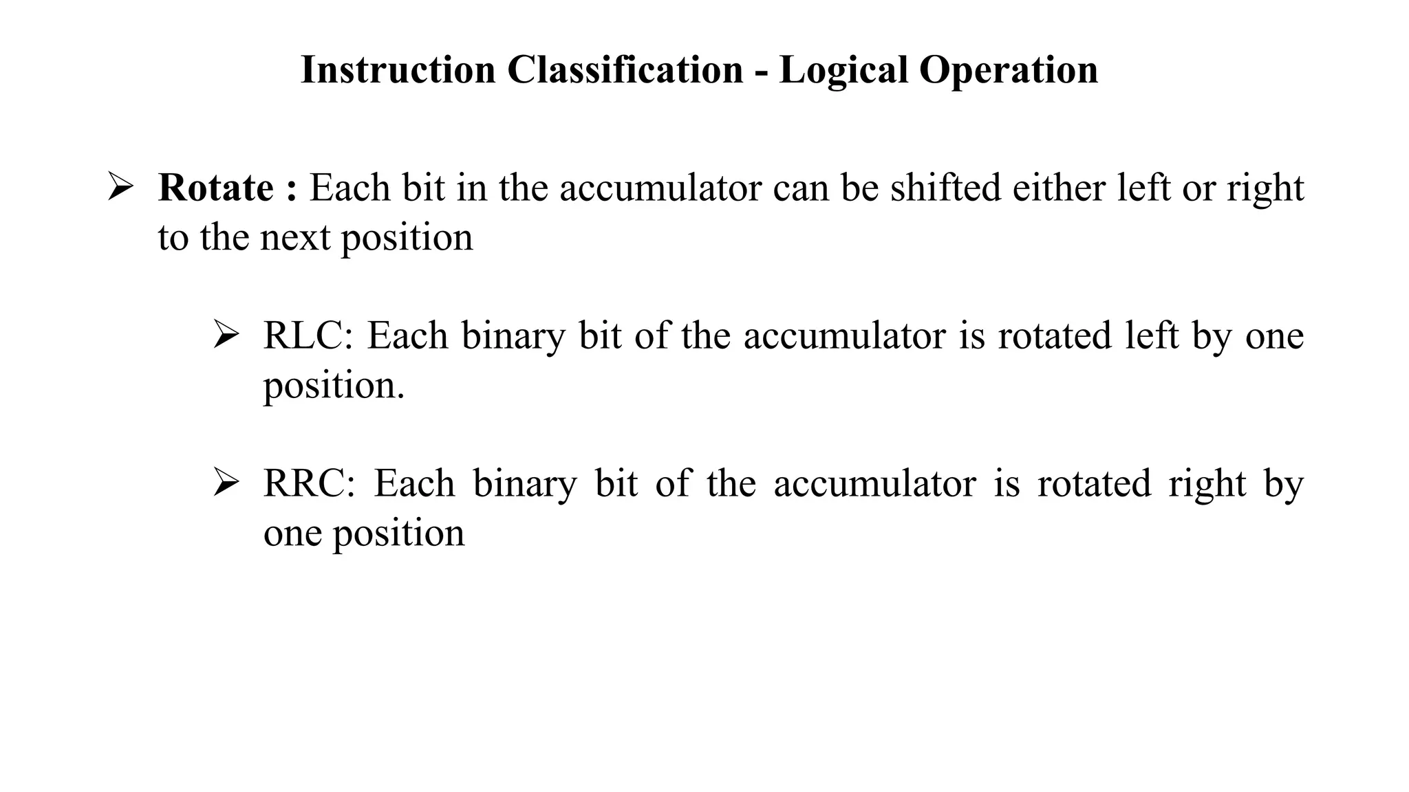
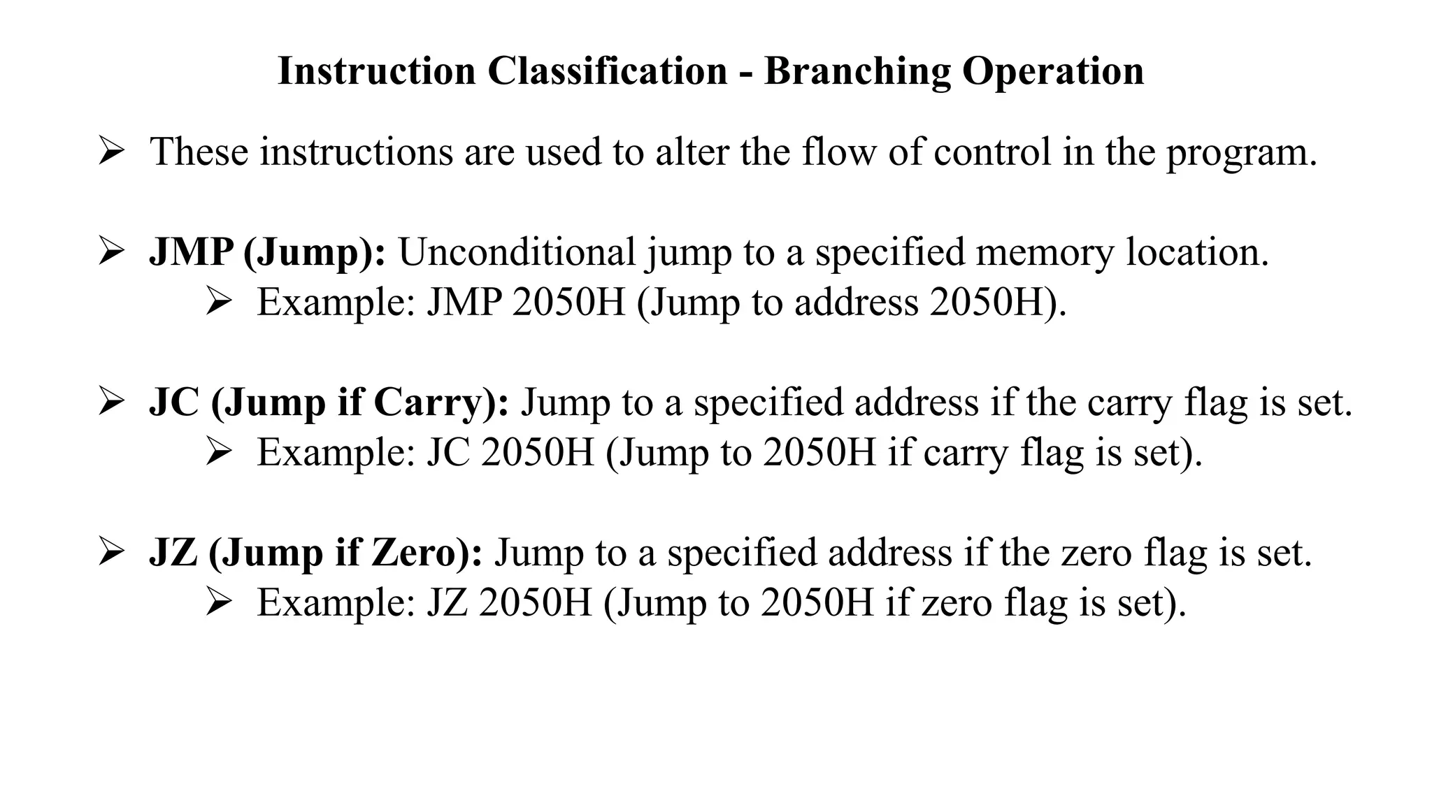
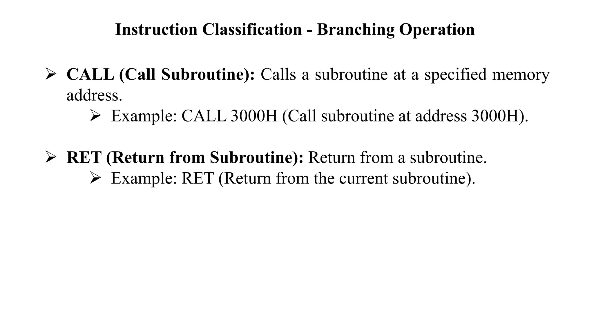
The 8085 MPU - The 8085 Pinout Signal - (Address bus, Data bus, Control and Status Signal, Power supply and frequency signal, Externally Initiated Signals, Serial I/O ports), Functional Block Diagram - (The ALU, Timing and control unit, Instruction Register and Decoder - Instruction Set - Instruction Classification - (Data Transfer operation- Arithmetic operations - logical operations - branching operations - machine control operations)
Previous Link:
Unit I : https://www.slideshare.net/slideshow/lecture-notes-microprocessor-unit-1-microprocessor-architecture-and-its-operation/274981732
Target Audience:
First year (Second Semester) B.Sc. Computer Science students at Alagappa University seeking a solid foundation in microprocessor and micro controller for academic and practical applications.
About the Author:
Dr. S. Murugan is Associate Professor at Alagappa Government Arts College, Karaikudi. With more than 20 years of teaching experience in the field of Computer Science, Dr. S. Murugan has a passion for simplifying complex concepts in microprocessor and micro controller.
Disclaimer:
This document is intended for educational purposes only. The content presented here reflects the author’s understanding in the field of Microprocessor and micro controller.