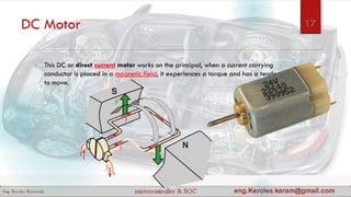
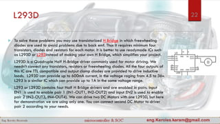
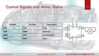
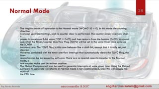
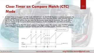
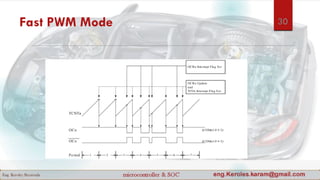
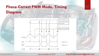
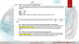
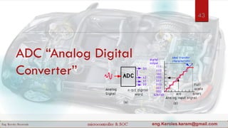
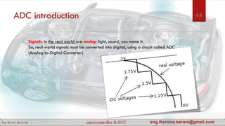
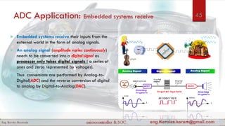
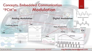
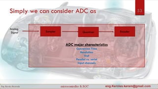
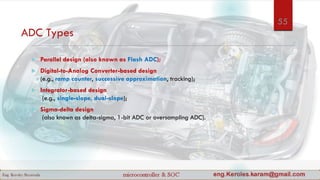
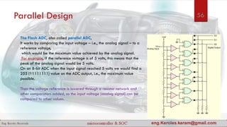
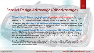
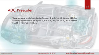
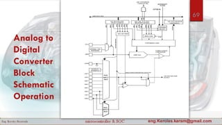
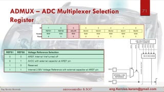
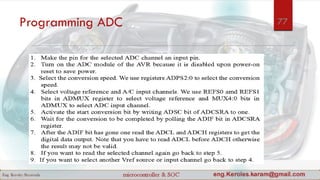
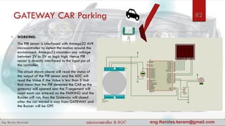
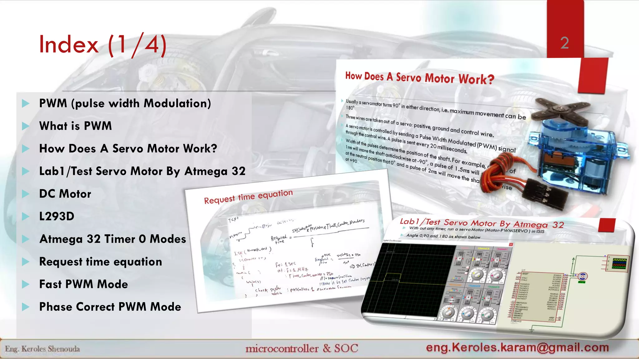
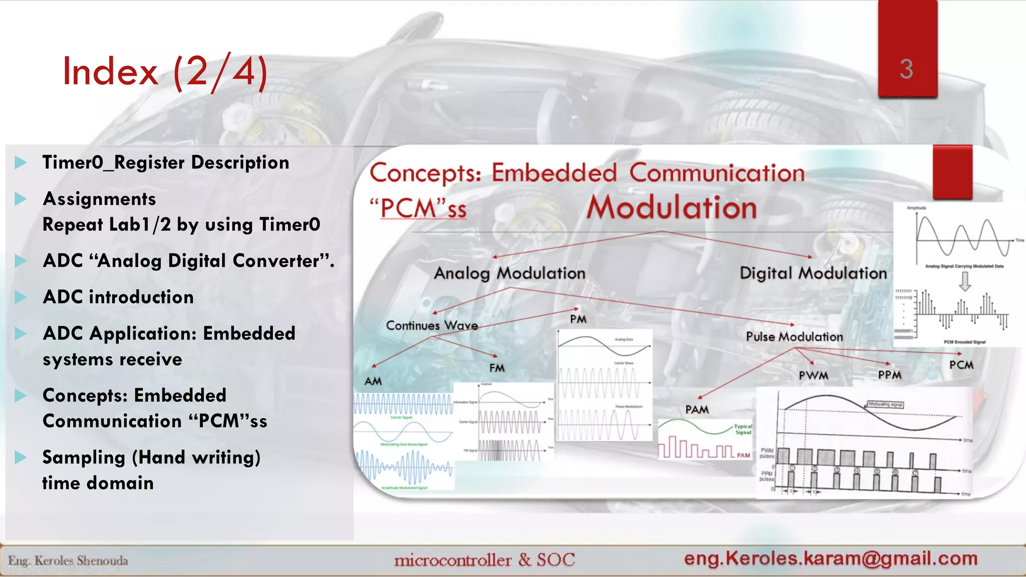
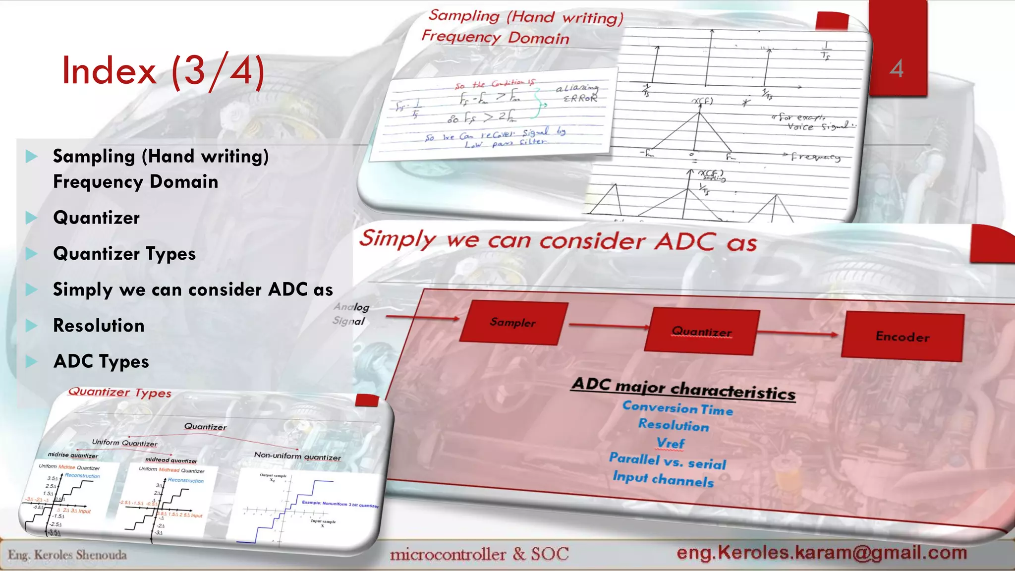
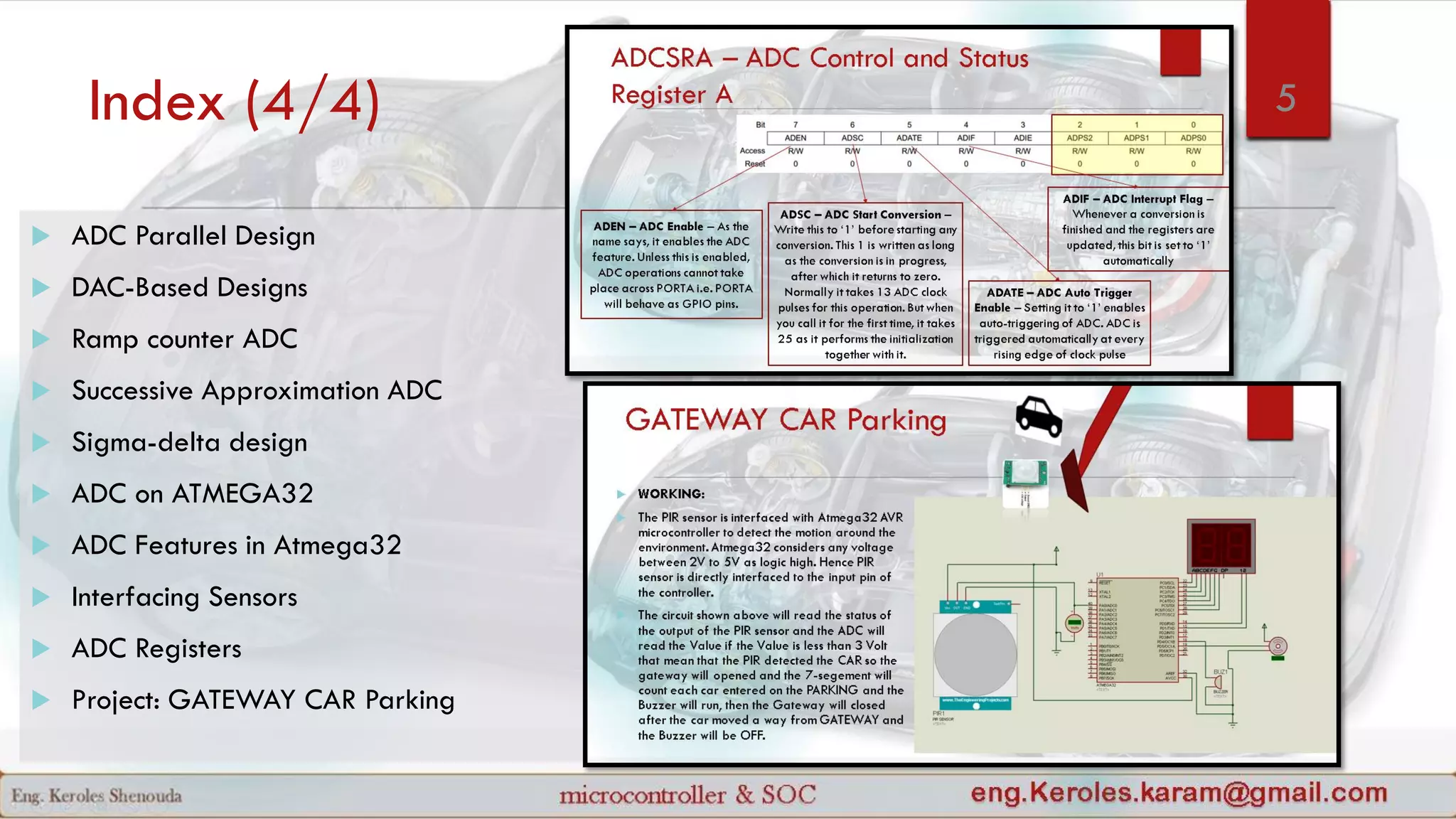
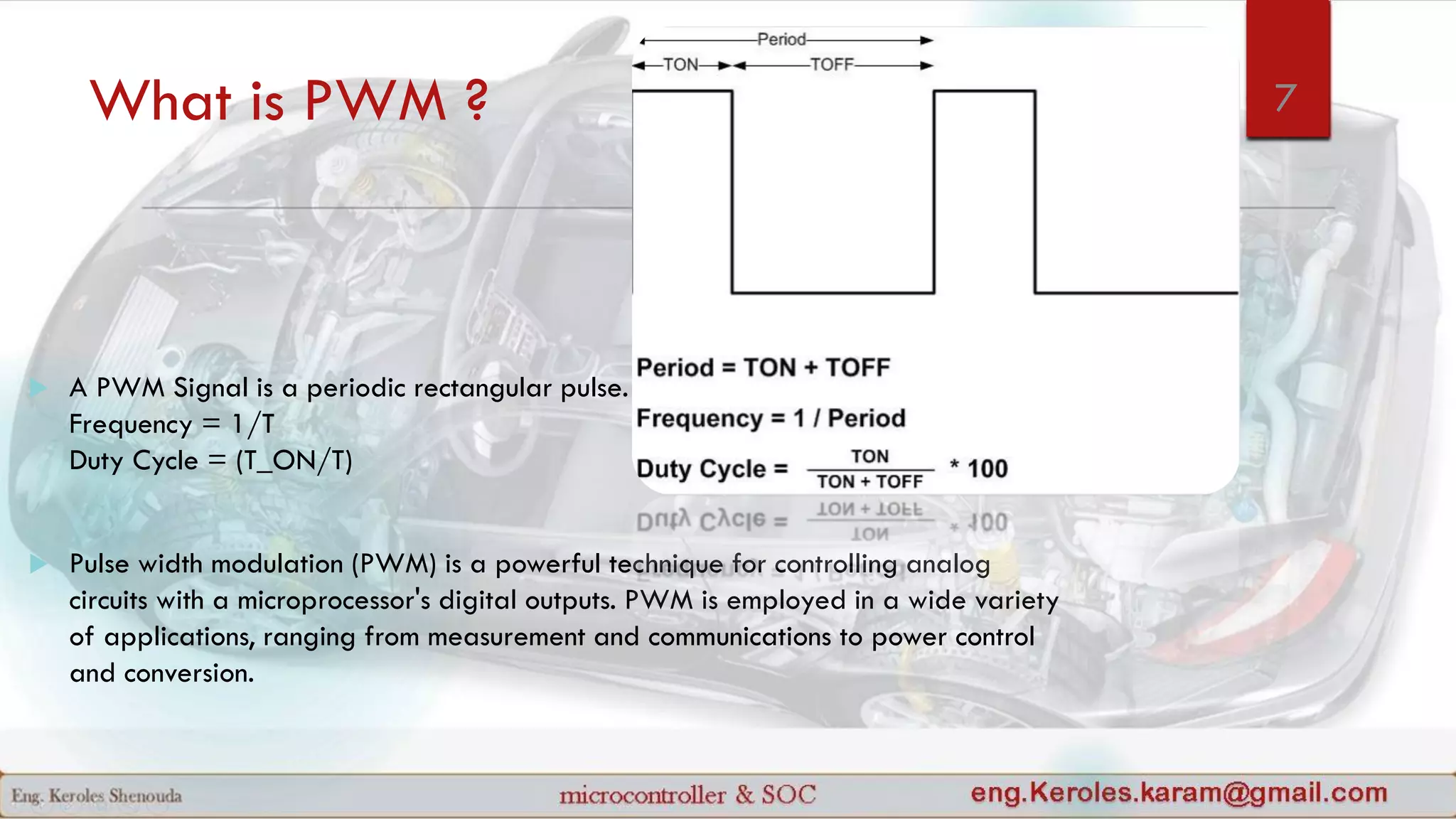
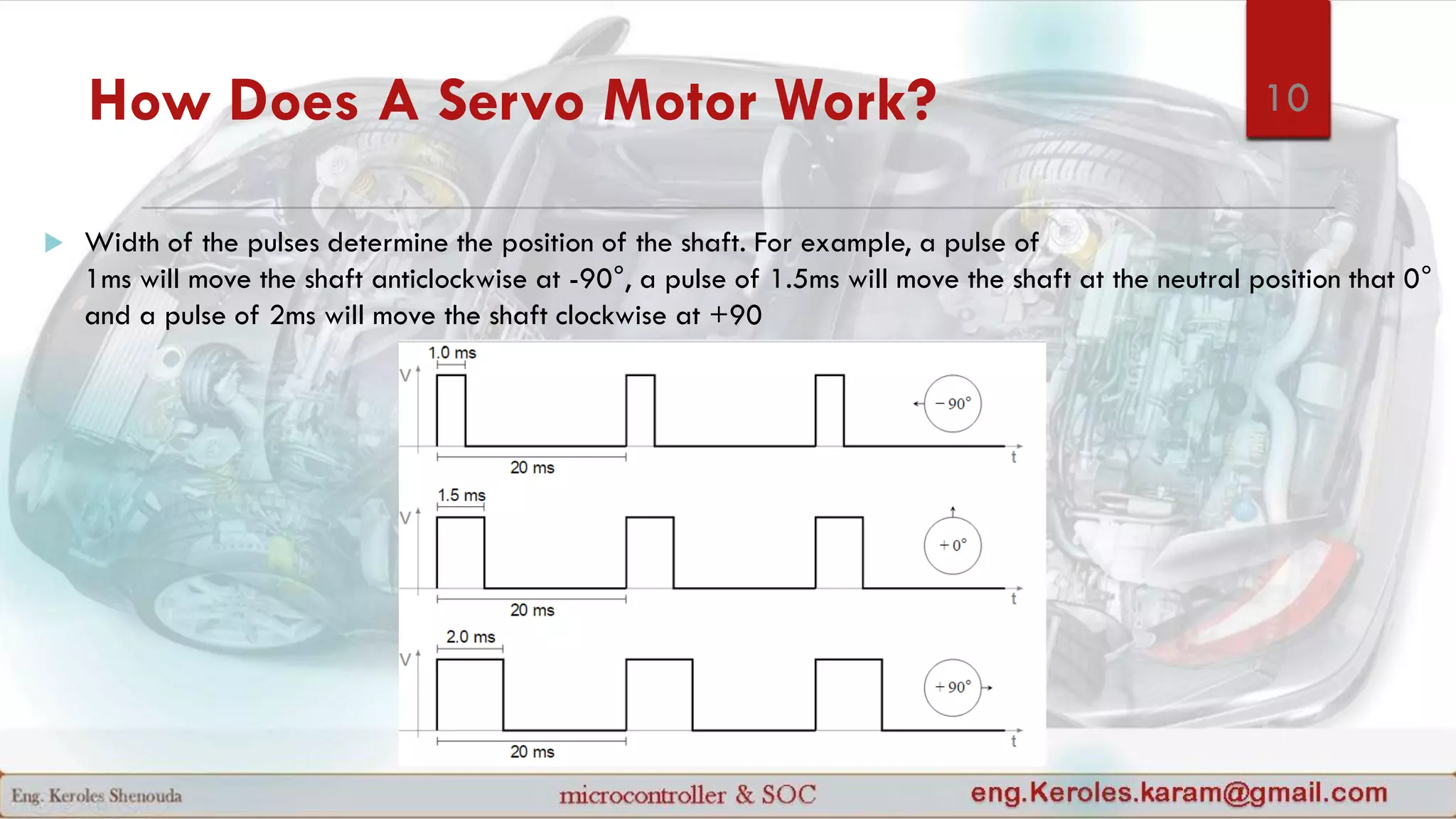
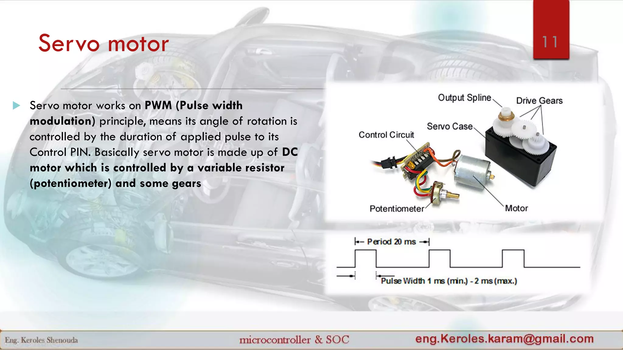
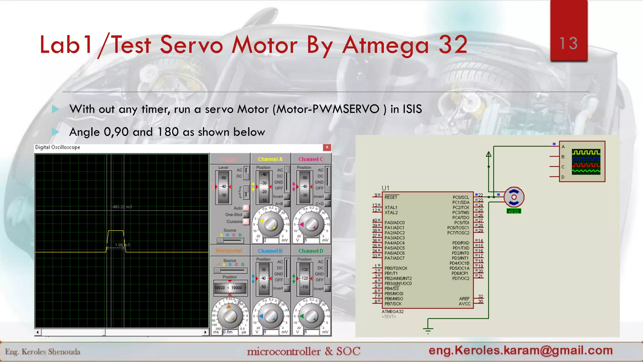
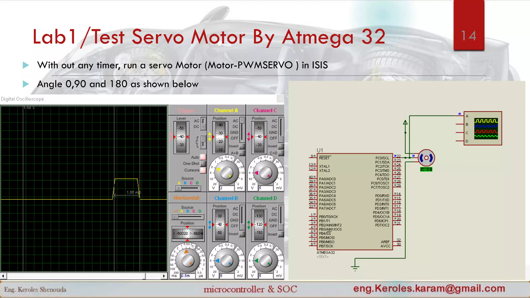
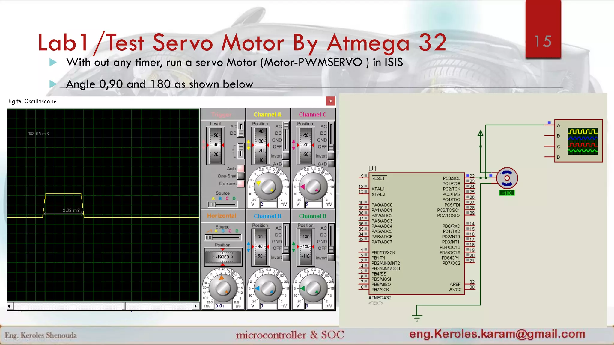
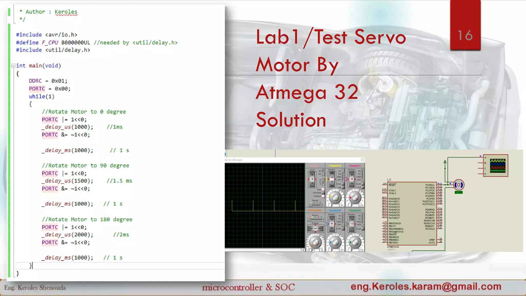
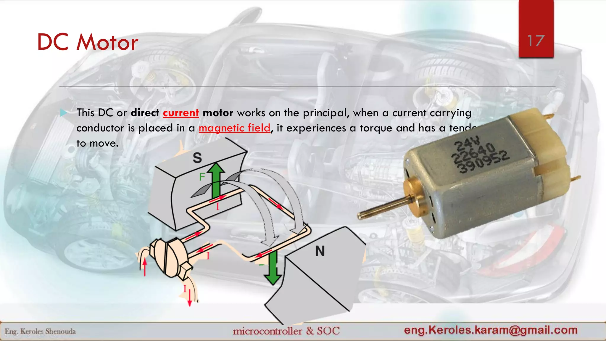
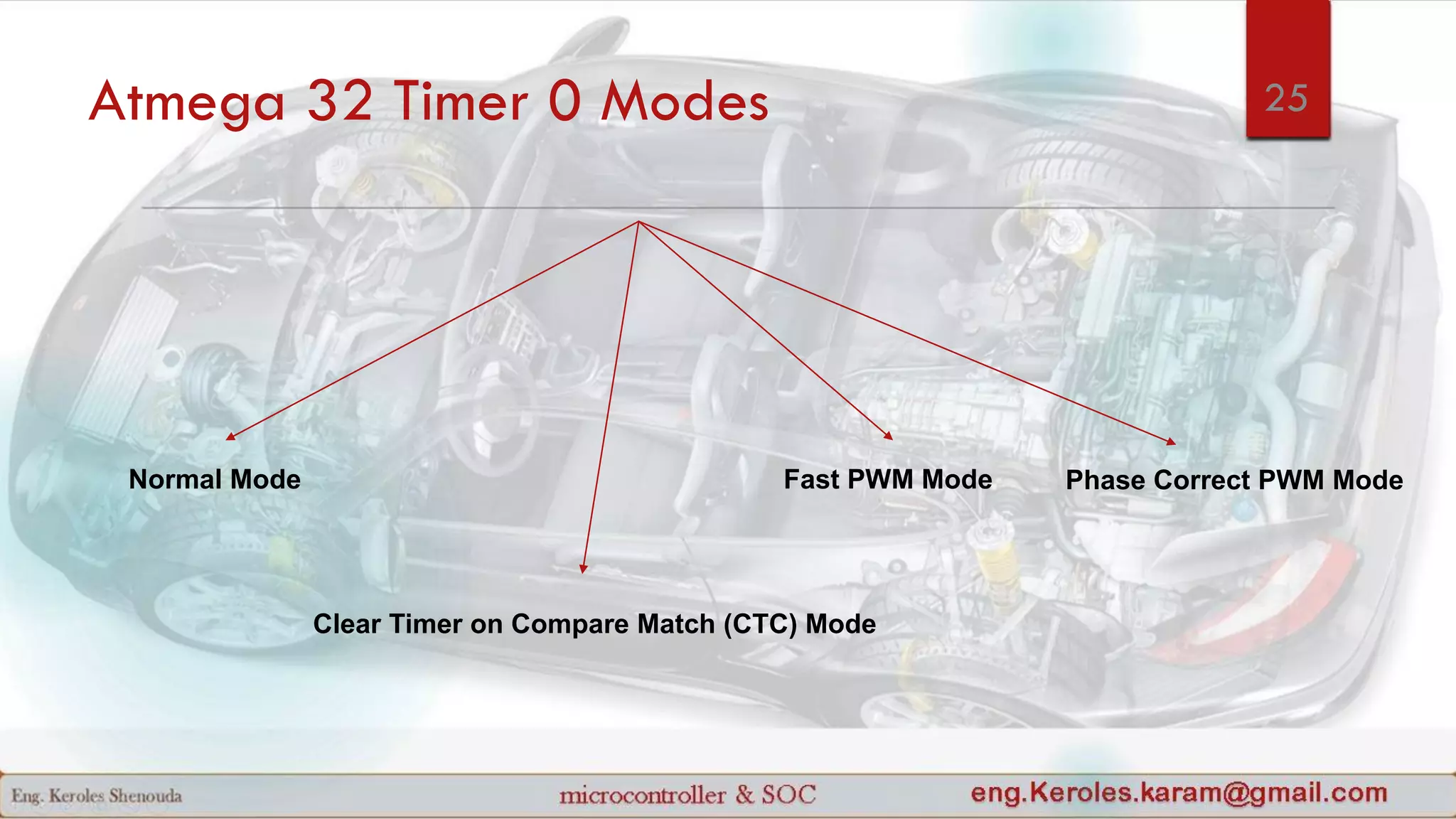
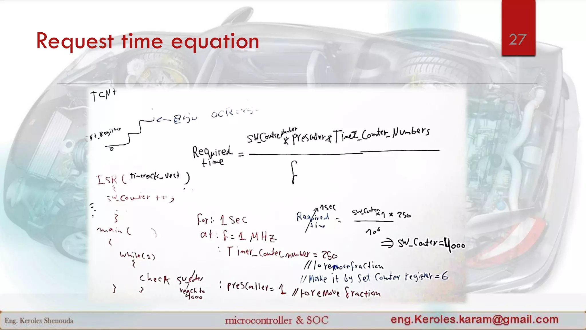
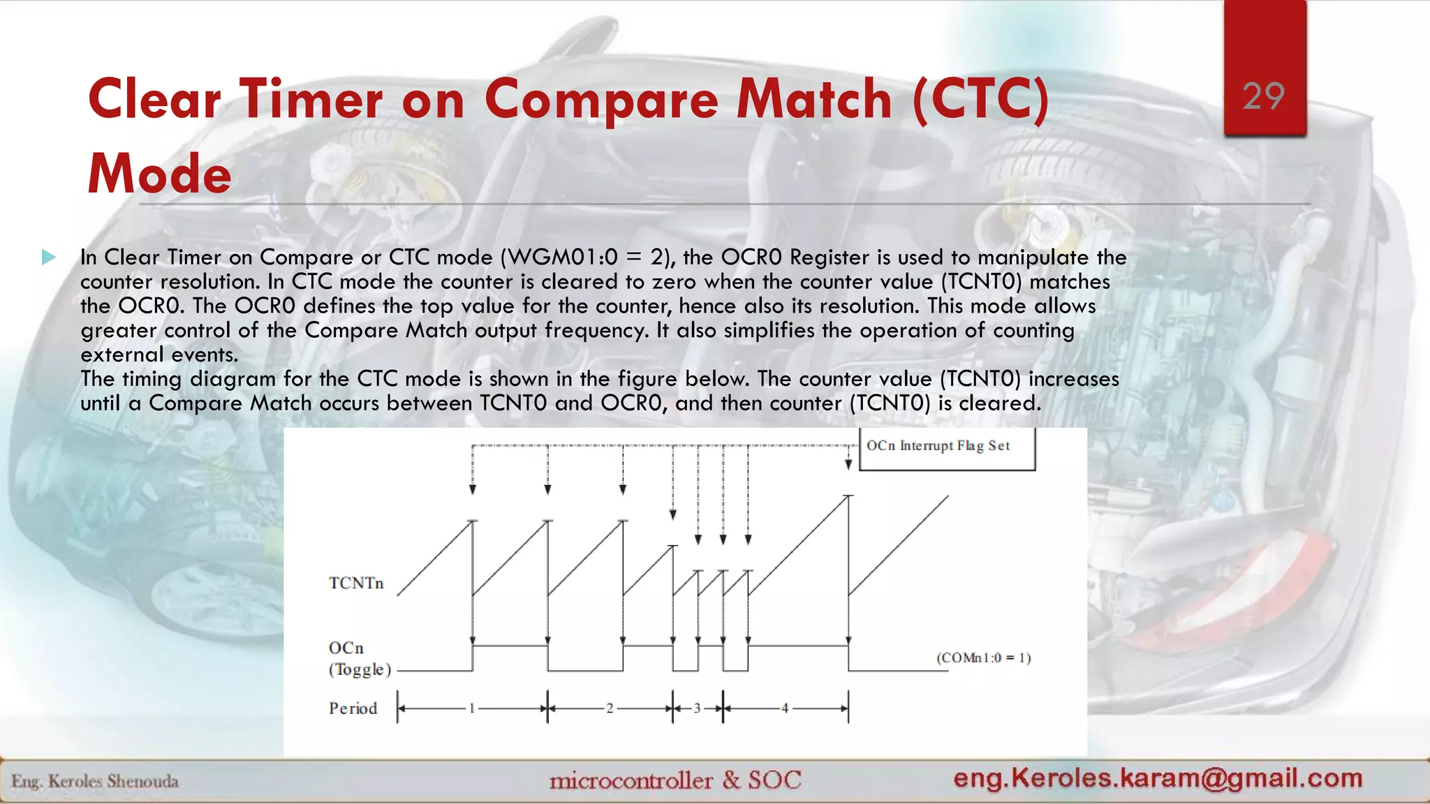
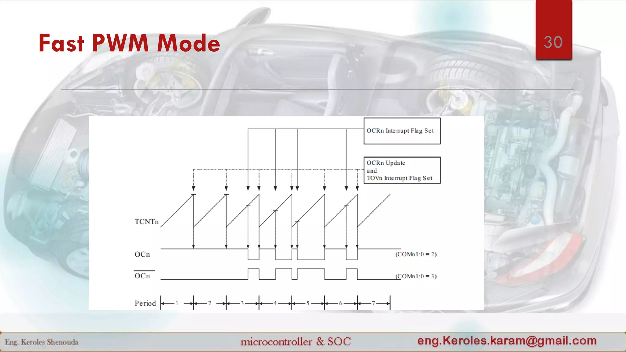
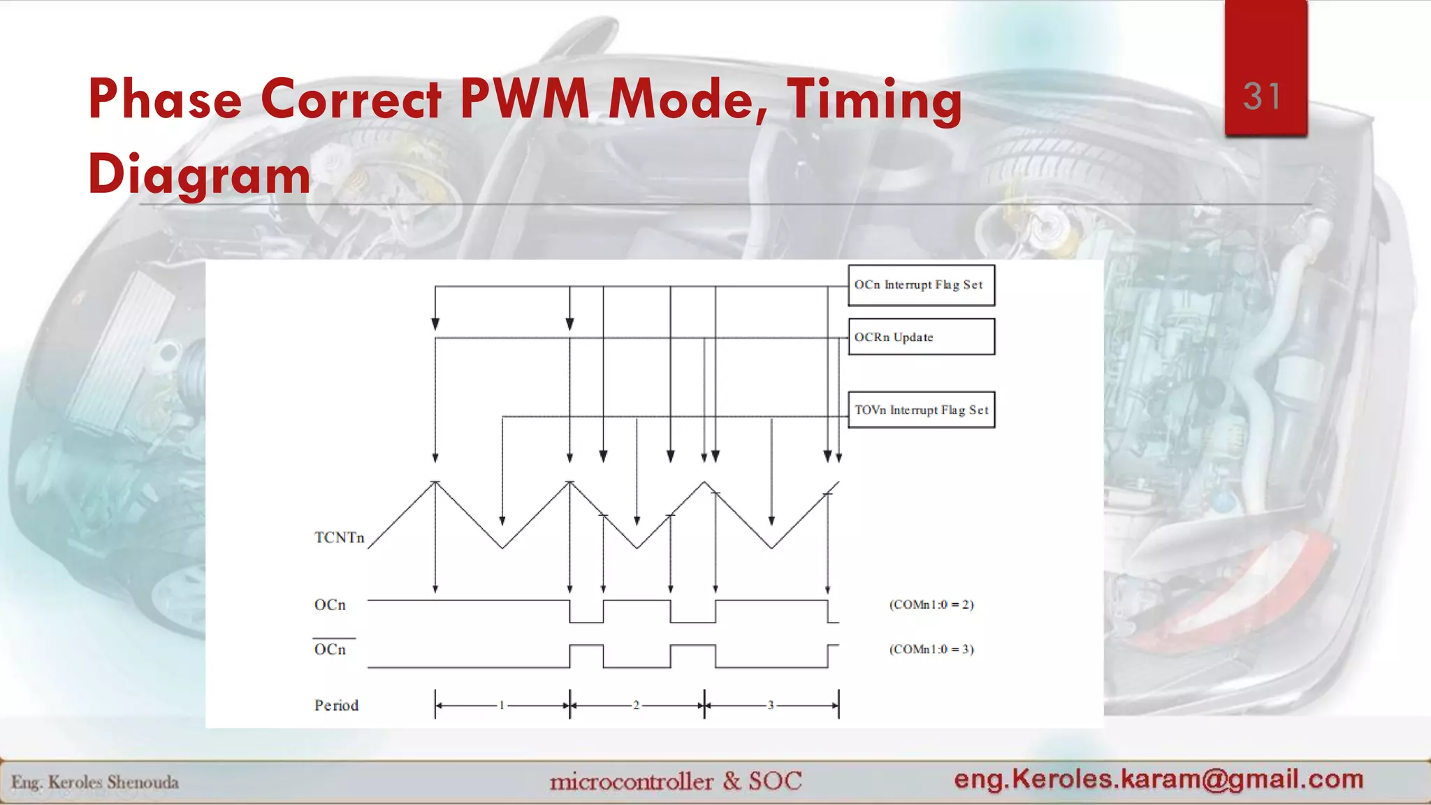
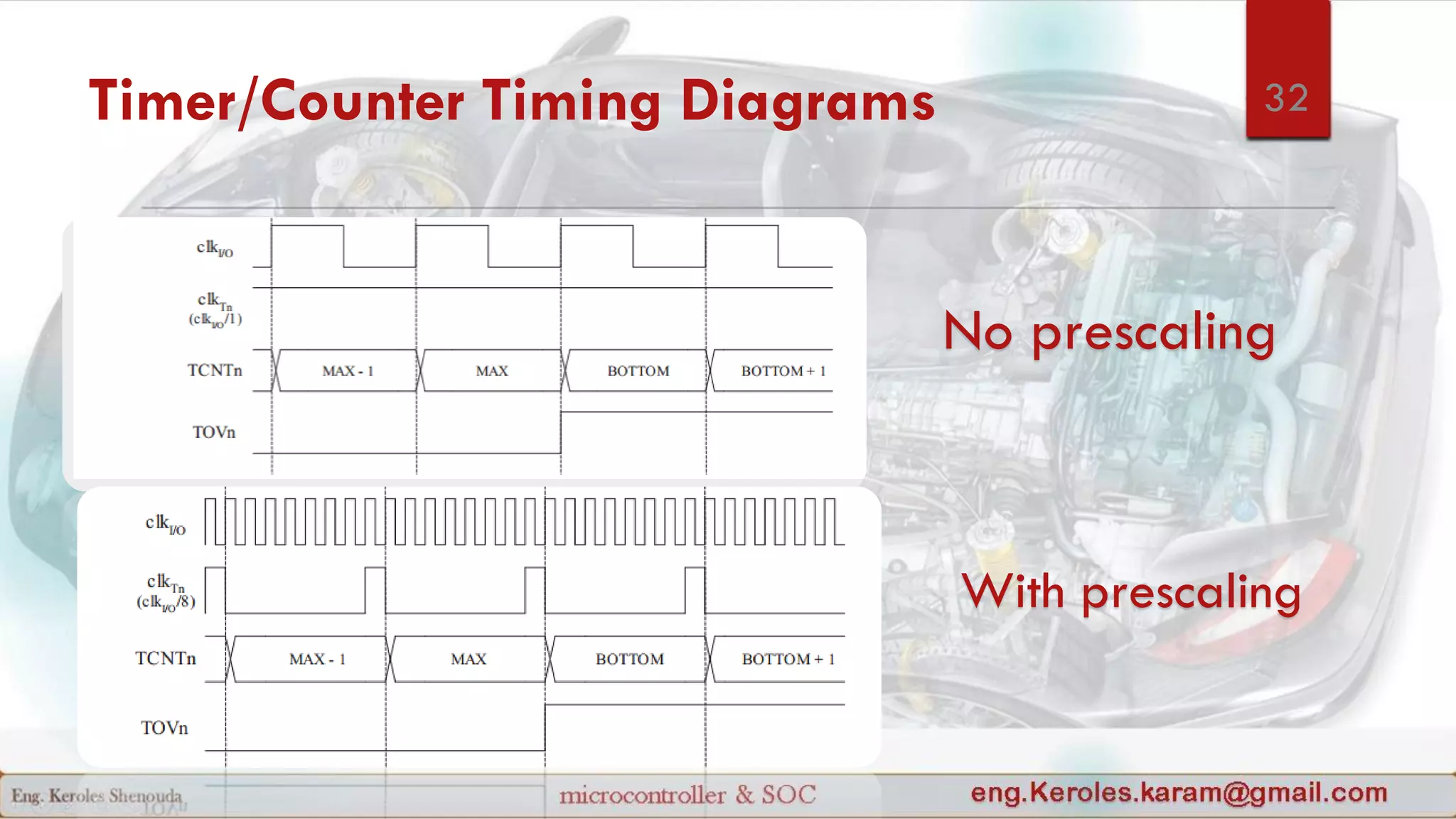
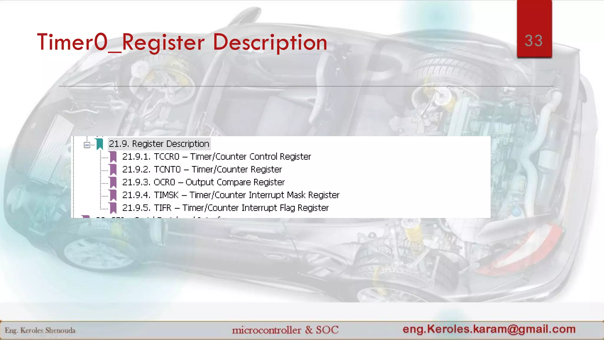
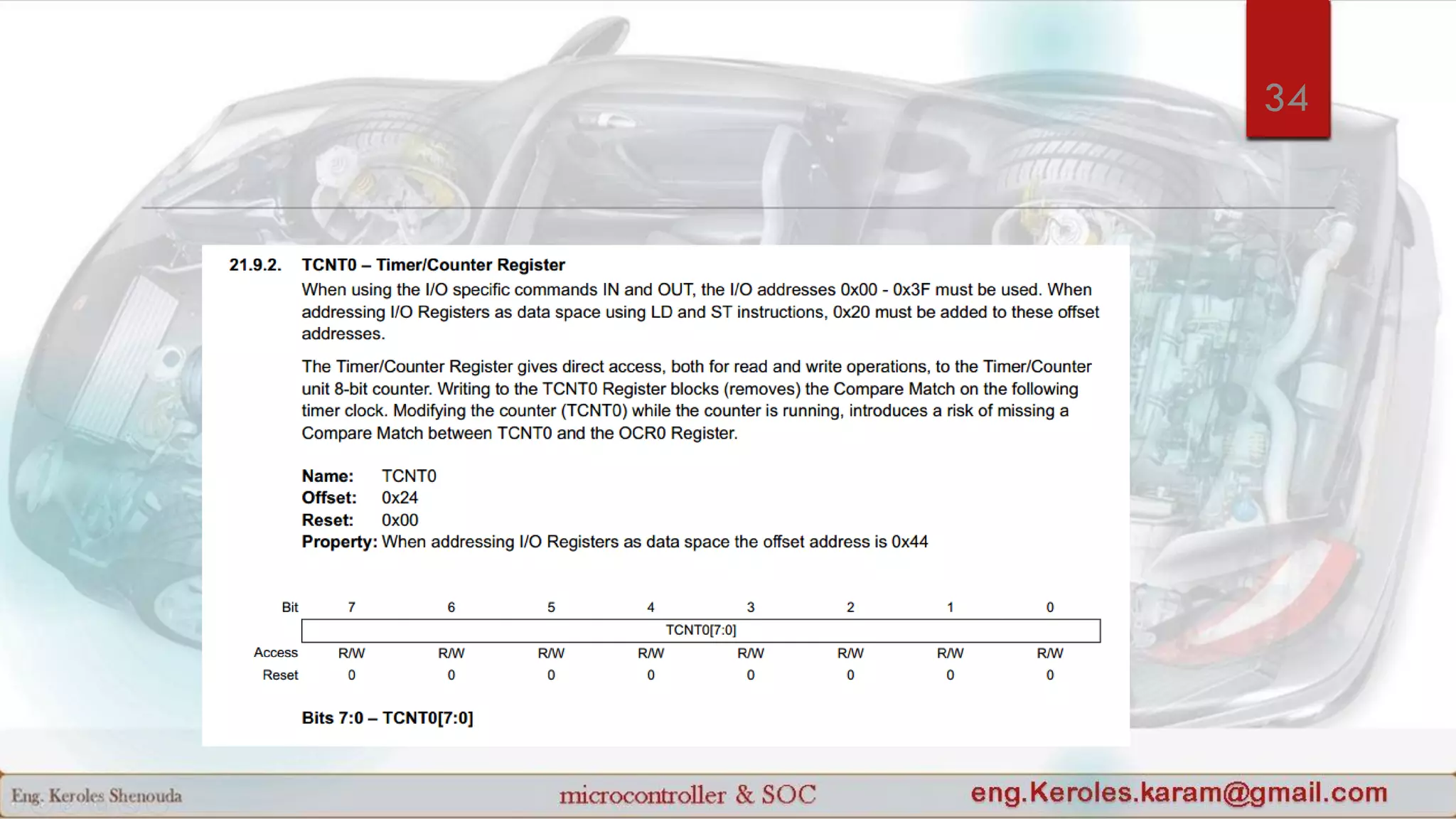
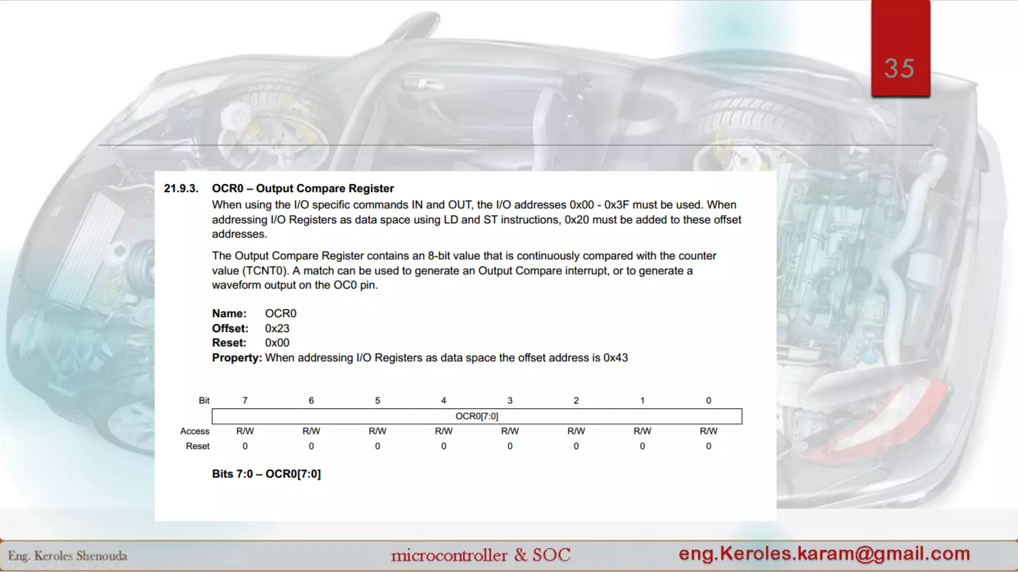
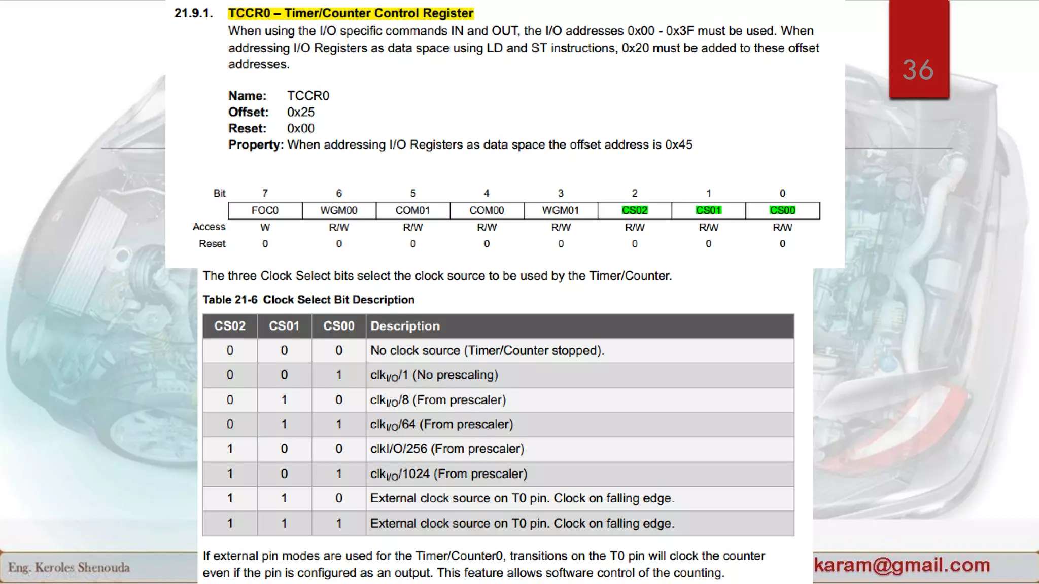
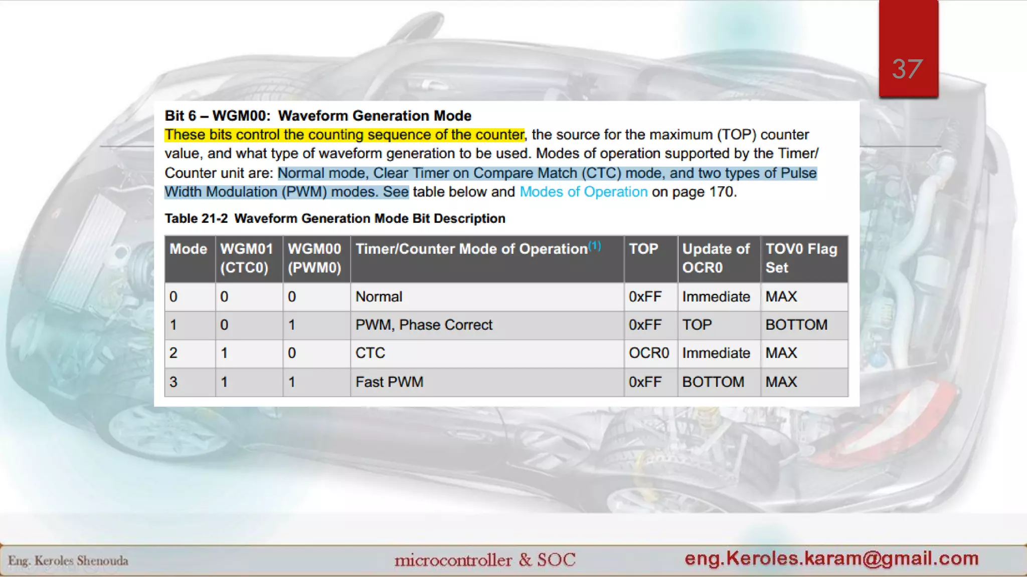
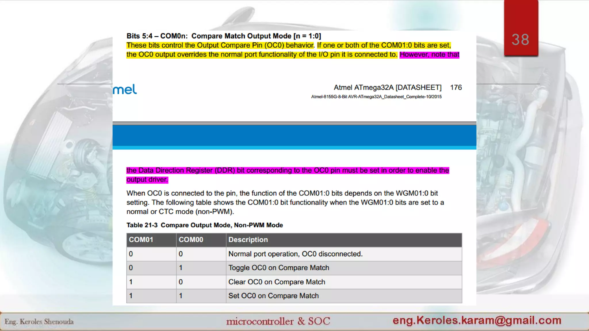
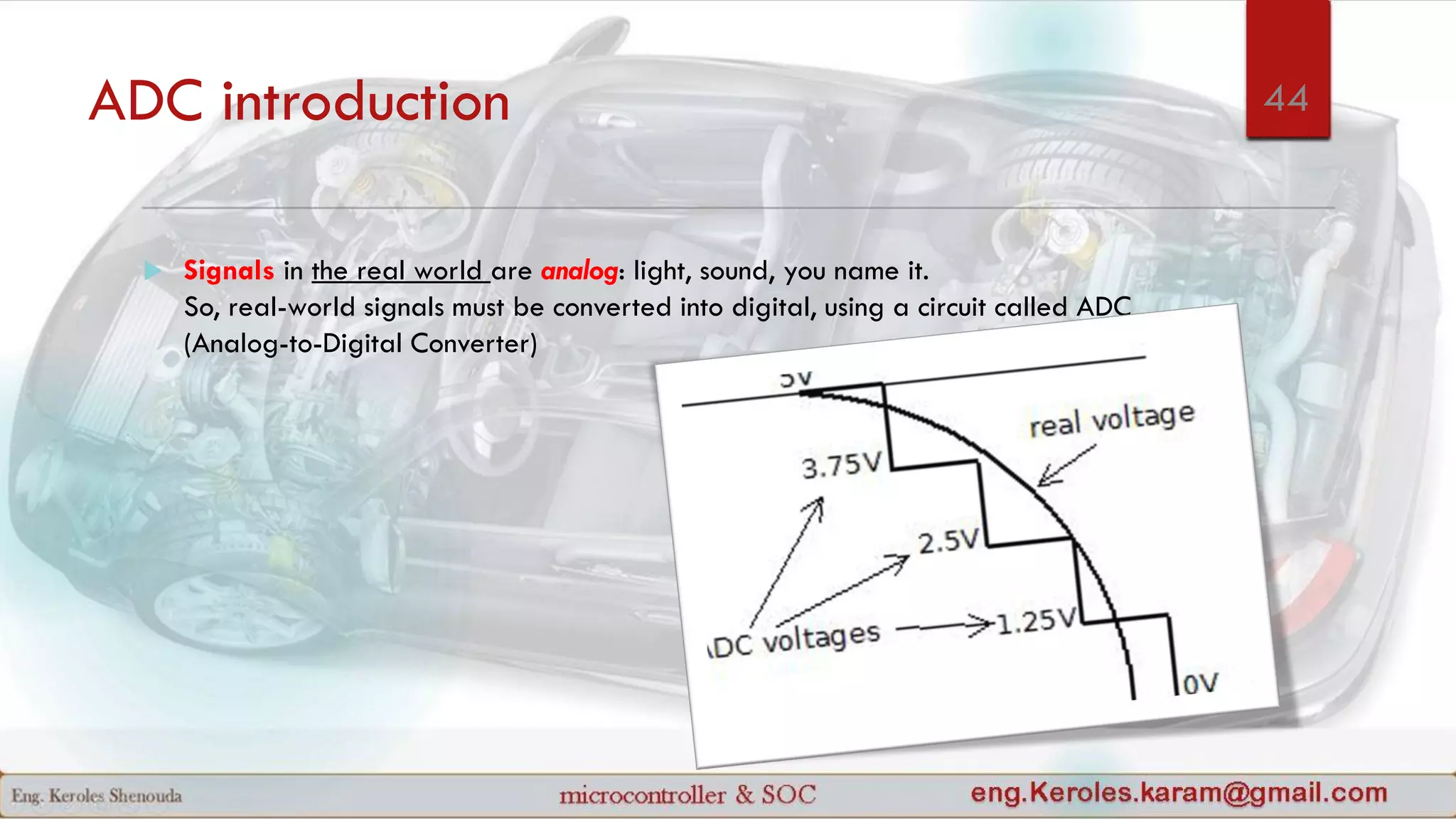
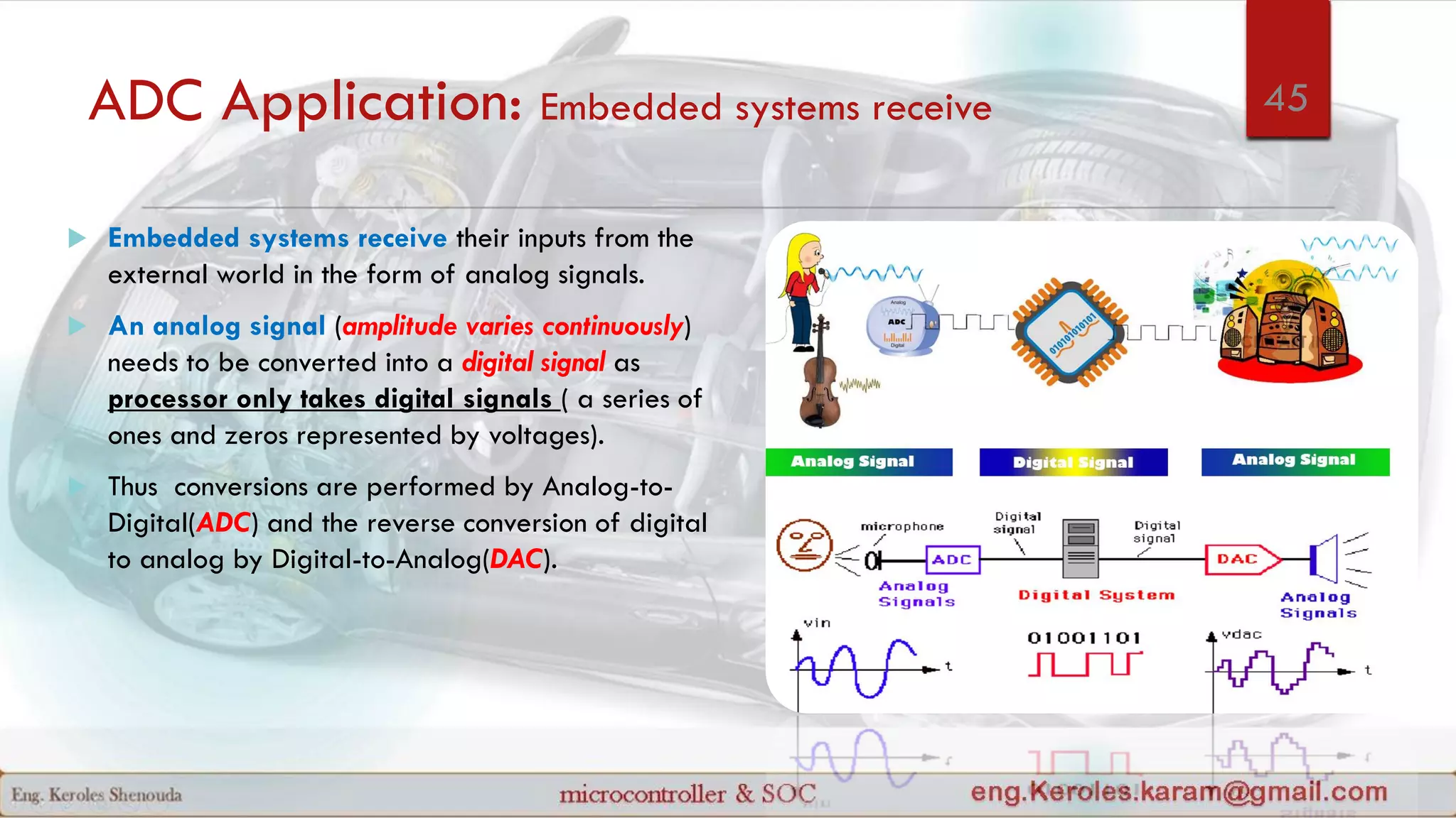
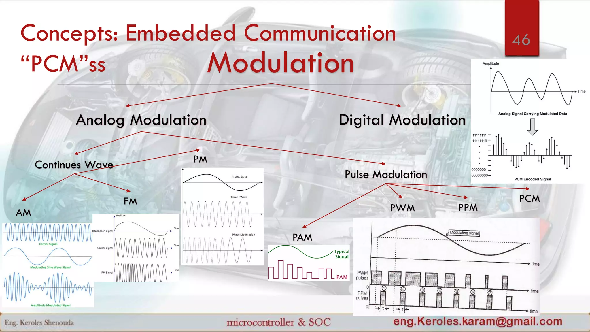
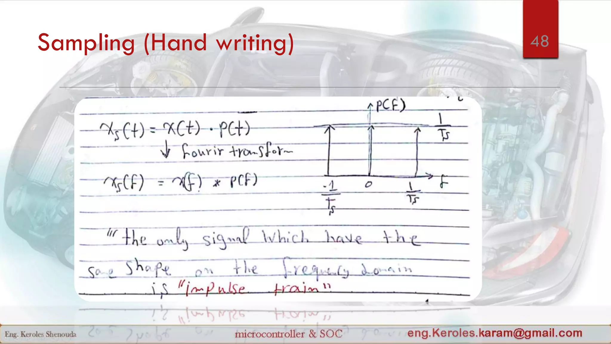
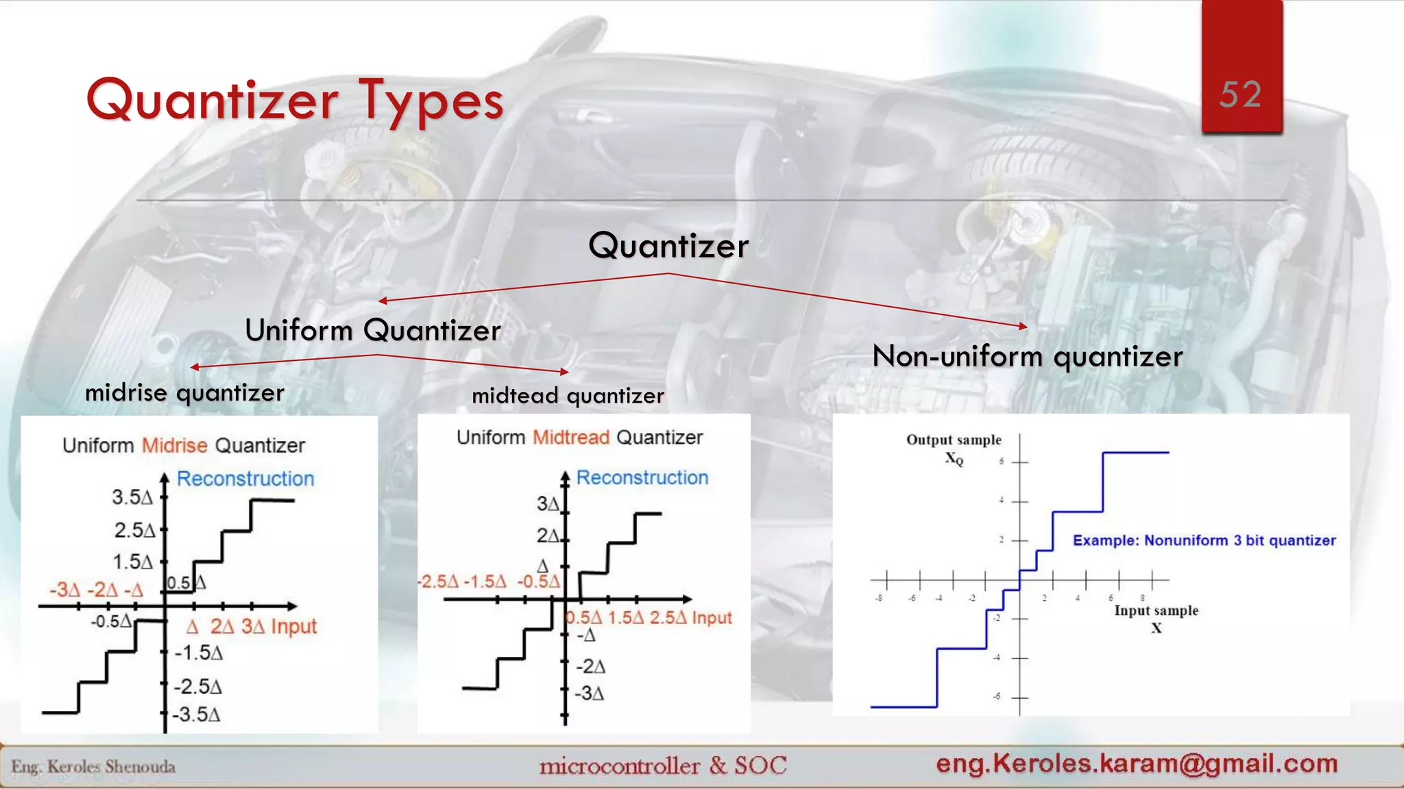
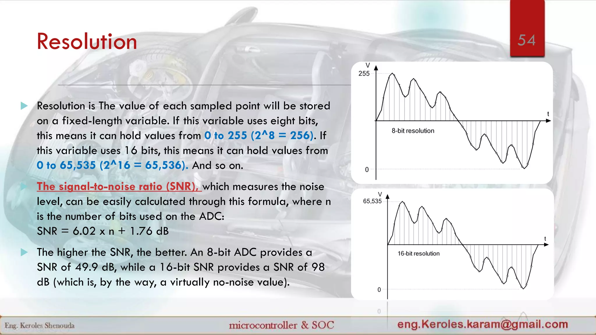
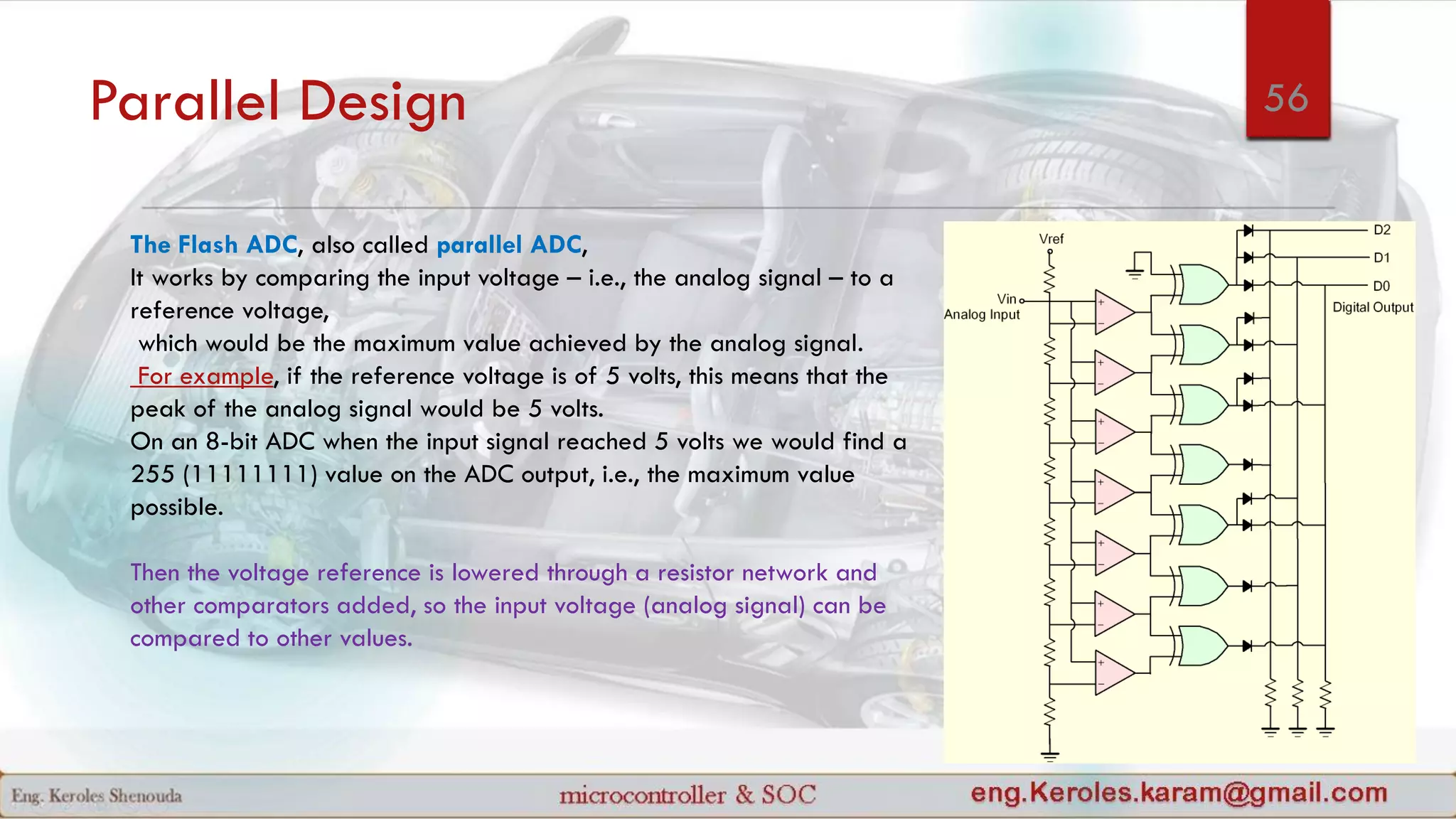
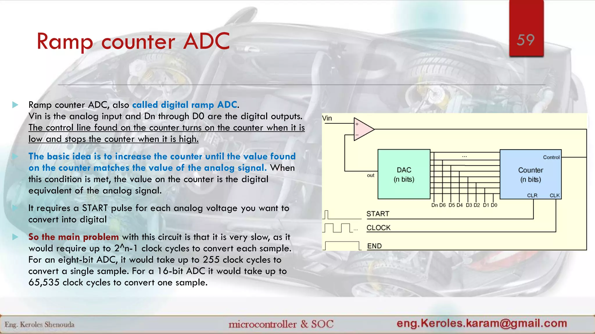
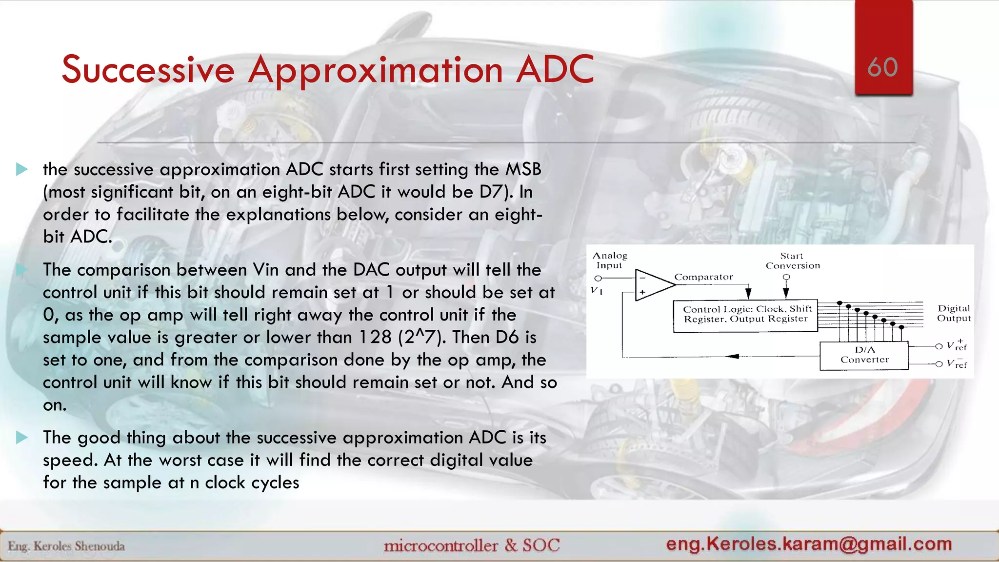
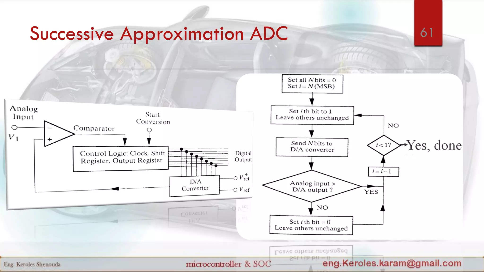
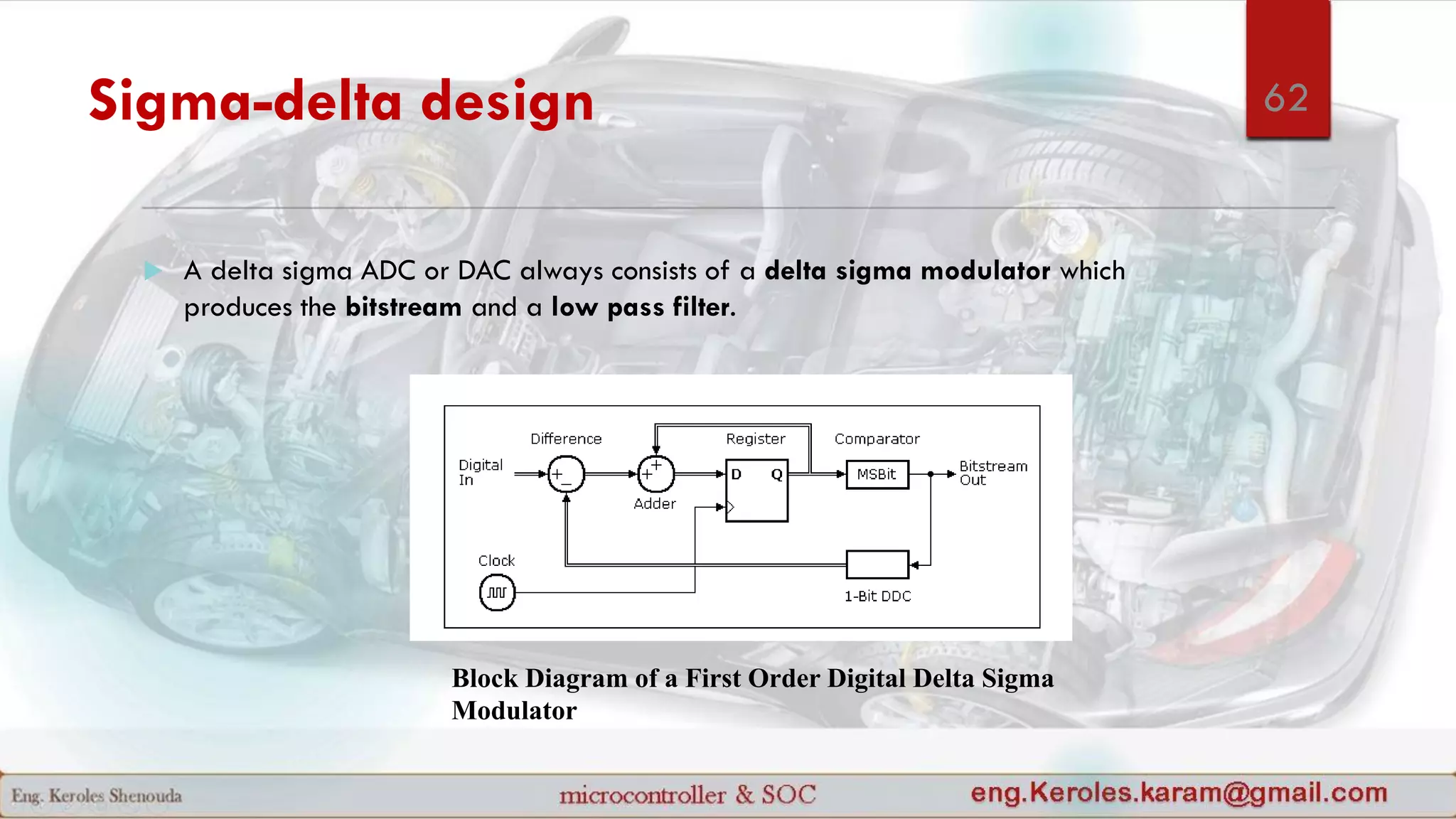
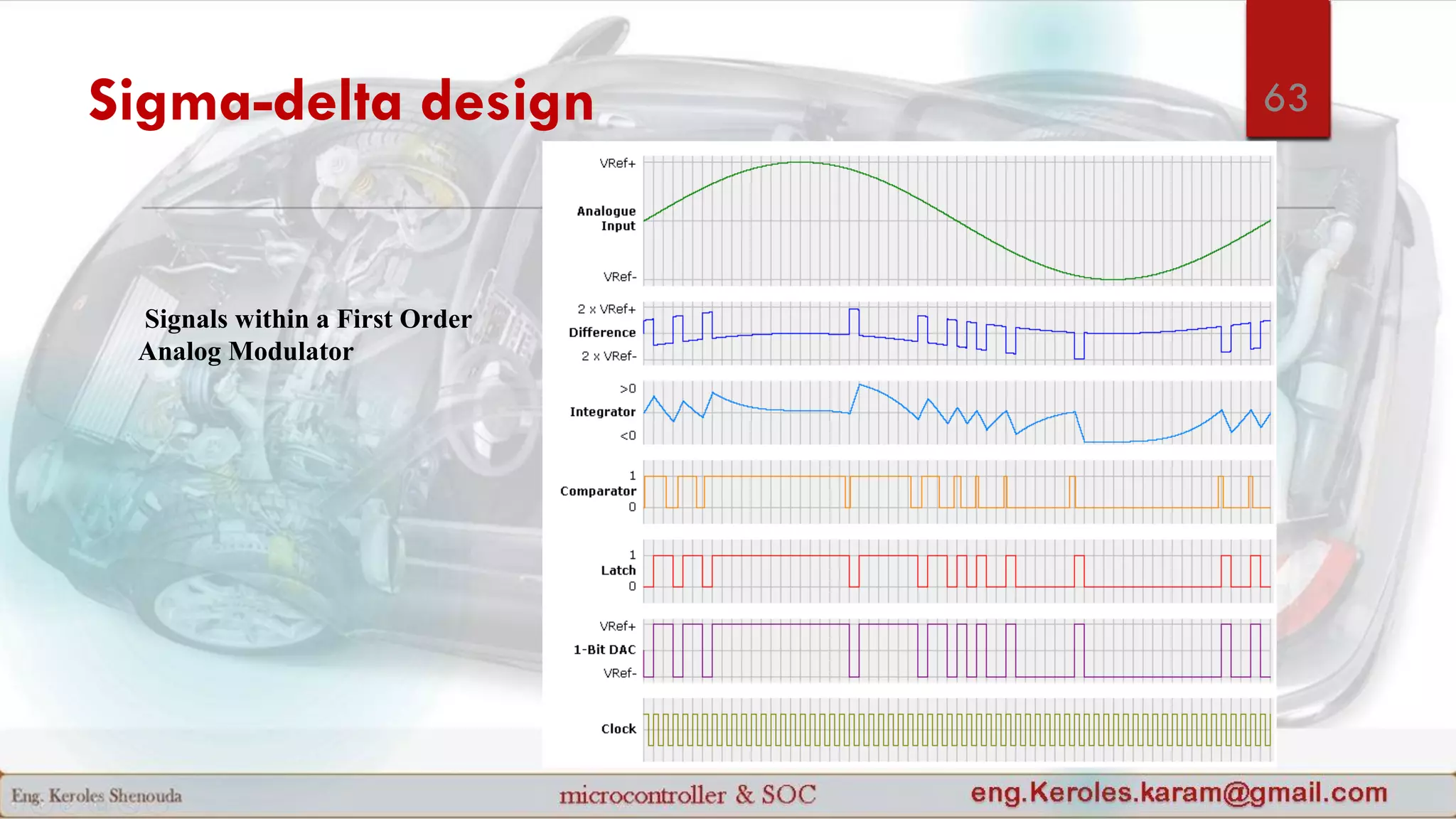
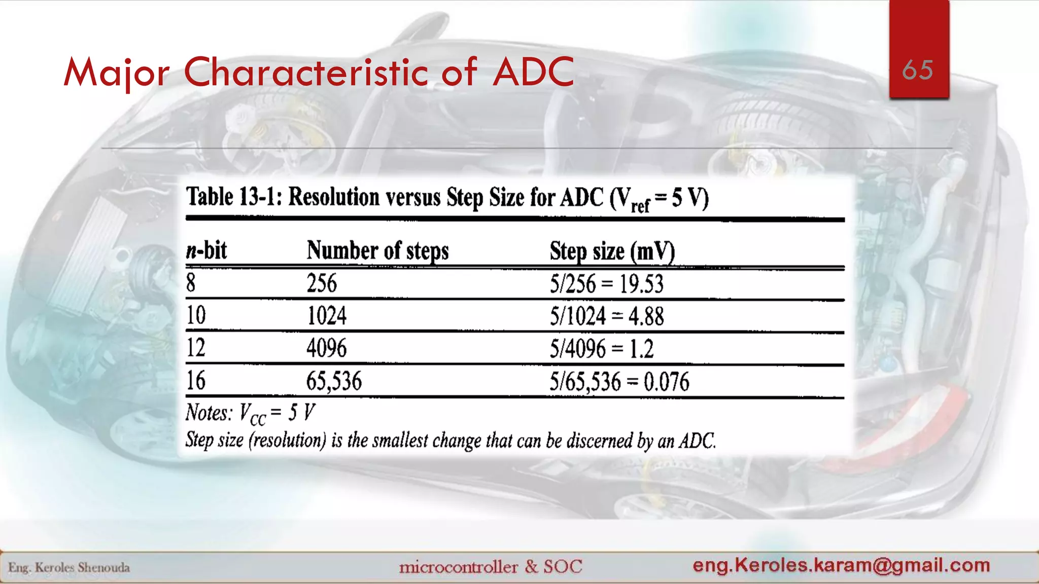
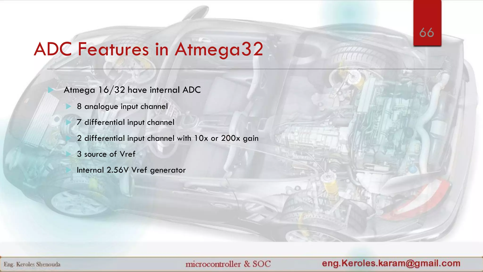
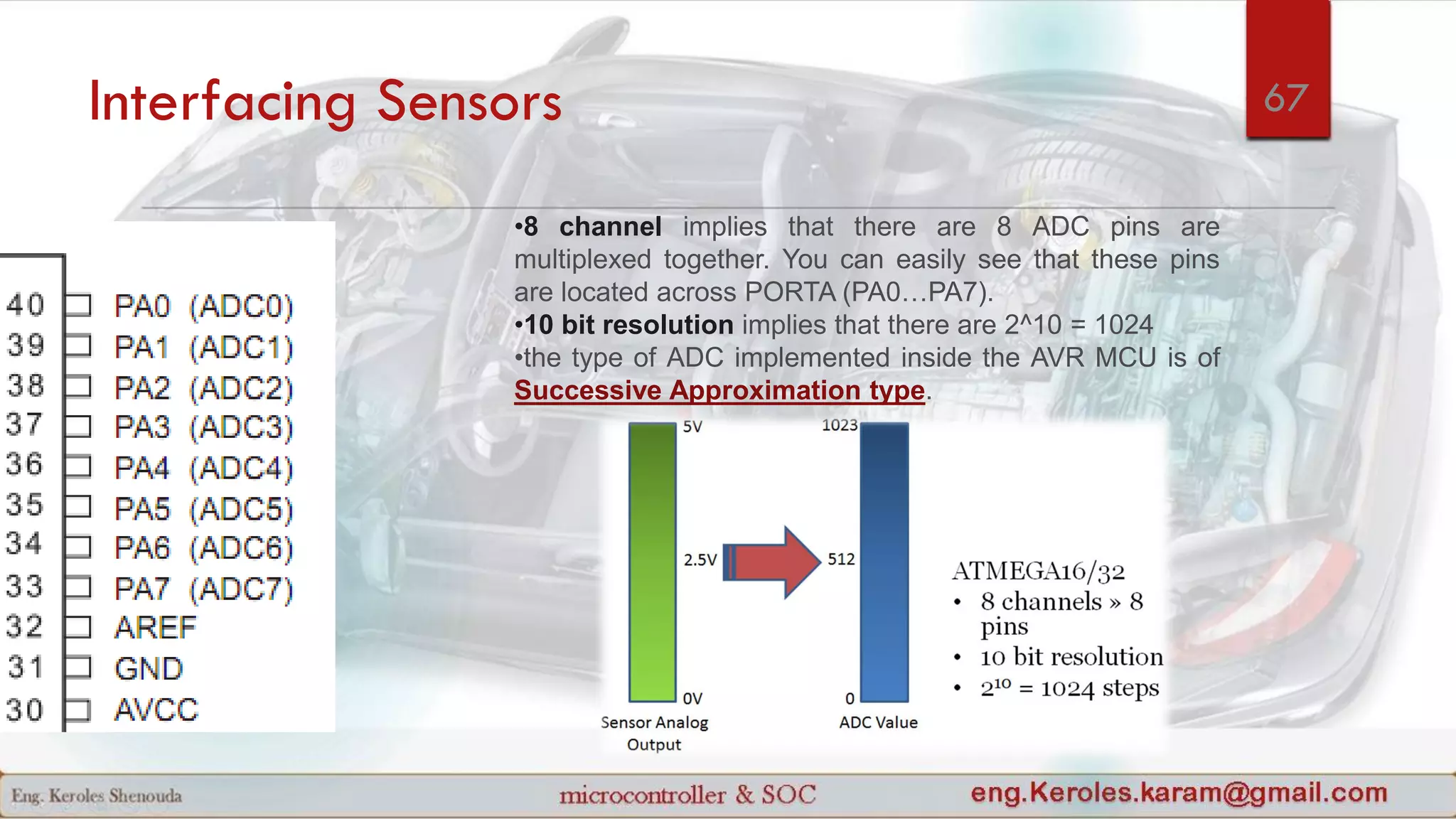
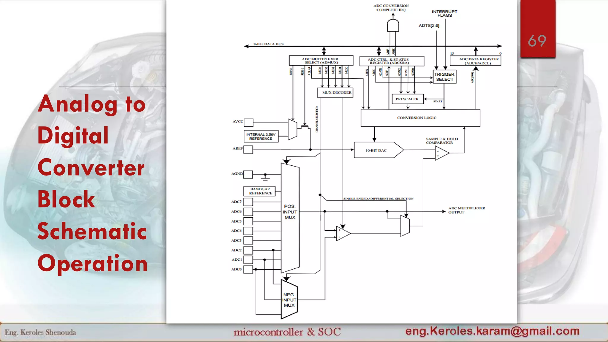
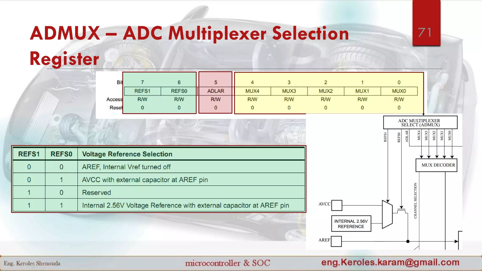
KEMBAR78
Microcontroller part 3 | PDF
Embedded System
ENG.KEROLES SHENOUDA
1
Index (1/4)
 PWM (pulse width Modulation)
 What is PWM
 How Does A Servo Motor Work?
 Lab1/Test Servo Motor By Atmega 32
 DC Motor
 L293D
 Atmega 32 Timer 0 Modes
 Request time equation
 Fast PWM Mode
 Phase Correct PWM Mode
2
Index (2/4) 3
 Timer0_Register Description
 Assignments
Repeat Lab1/2 by using Timer0
 ADC “Analog Digital Converter”.
 ADC introduction
 ADC Application: Embedded
systems receive
 Concepts: Embedded
Communication “PCM”ss
 Sampling (Hand writing)
time domain
Index (3/4) 4
 Sampling (Hand writing)
Frequency Domain
 Quantizer
 Quantizer Types
 Simply we can consider ADC as
 Resolution
 ADC Types
Index (4/4) 5
 ADC Parallel Design
 DAC-Based Designs
 Ramp counter ADC
 Successive Approximation ADC
 Sigma-delta design
 ADC on ATMEGA32
 ADC Features in Atmega32
 Interfacing Sensors
 ADC Registers
 Project: GATEWAY CAR Parking
PWM (pulse width
Modulation)
6
What is PWM ?
 A PWM Signal is a periodic rectangular pulse.
Frequency = 1/T
Duty Cycle = (T_ON/T)
 Pulse width modulation (PWM) is a powerful technique for controlling analog
circuits with a microprocessor's digital outputs. PWM is employed in a wide variety
of applications, ranging from measurement and communications to power control
and conversion.
7
What is need of PWM?
 PWM is mainly used for controlling the speed of DC motors . By pulse width
modulation we can get a variable voltage digitally, that is we get voltages
between 0 and VCC by switching the VCC on and off periodically . Other
applications are fading Led , getting different tones in Buzzer,Contolling the
degree of rotation of Servo motor .
8
How Does A Servo Motor Work?
 Usually a servomotor turns 90° in either direction, i.e. maximum movement can be
180°
 Three wires are taken out of a servo: positive, ground and control wire.
 A servo motor is controlled by sending a Pulse Width Modulated (PWM) signal
through the control wire. A pulse is sent every 20 milliseconds.
 Width of the pulses determine the position of the shaft. For example, a pulse of
1ms will move the shaft anticlockwise at -90°, a pulse of 1.5ms will move the shaft
at the neutral position that 0° and a pulse of 2ms will move the shaft clockwise
at +90
9
How Does A Servo Motor Work?
 Width of the pulses determine the position of the shaft. For example, a pulse of
1ms will move the shaft anticlockwise at -90°, a pulse of 1.5ms will move the shaft at the neutral position that 0°
and a pulse of 2ms will move the shaft clockwise at +90
10
Servo motor
 Servo motor works on PWM (Pulse width
modulation) principle, means its angle of rotation is
controlled by the duration of applied pulse to its
Control PIN. Basically servo motor is made up of DC
motor which is controlled by a variable resistor
(potentiometer) and some gears
11
Servo motor (another degree
range)(Motor-PWMSERVO in ISIS)
 Servo motor can be rotated from 0 to
180 degree, but it can go up to 210
degree, depending on the
manufacturing. This degree of rotation
can be controlled by applying
the Electrical Pulse of proper width,
to its Control pin. Servo checks the
pulse in every 20 milliseconds. Pulse
of 1 ms (1 millisecond) width can
rotate servo to 0 degree, 1.5ms can
rotate to 90 degree (neutral position)
and 2 ms pulse can rotate it to 180
degree.
12
Lab1/Test Servo Motor By Atmega 32
 With out any timer, run a servo Motor (Motor-PWMSERVO ) in ISIS
 Angle 0,90 and 180 as shown below
13
Lab1/Test Servo Motor By Atmega 32
 With out any timer, run a servo Motor (Motor-PWMSERVO ) in ISIS
 Angle 0,90 and 180 as shown below
14
Lab1/Test Servo Motor By Atmega 32
 With out any timer, run a servo Motor (Motor-PWMSERVO ) in ISIS
 Angle 0,90 and 180 as shown below
15
Lab1/Test Servo
Motor By
Atmega 32
Solution
16
DC Motor
 This DC or direct current motor works on the principal, when a current carrying
conductor is placed in a magnetic field, it experiences a torque and has a tendency
to move.
17
Lab2/ write embedded C Code without
timer to run two DC Motors
 First DC Motor Connect to PD0 (run Clockwise)
 Second DC Motor Connect to PD1 (run Anticlockwise)
 Sequence (Motor 1 run) > Motor1 stop & Motor 2 run
And so on
 Choose the time you prefer
18
Lab2/ sequence 19
LAB2/Solution 20
We can’t connect a DC Motor directly to a
microcontroller ?
 A microcontroller can’t supply the current required for the working of DC
Motor. ATmega32 Microcontroller can source or sink currents up to 40mA but a DC
Motor needs current very much more than that.
 The negative voltages created due to the back emf of the motor may affect the
proper functioning of the microcontroller.
 You may need to control the direction of rotation of the motor by changing the
polarity of the motor supply.
 The operating voltage of the DC Motor may be much higher than the operating
voltage of the microcontroller.
21
L293D
 To solve these problems you may use transistorized H Bridge in which freewheeling
diodes are used to avoid problems due to back emf. Thus it requires minimum four
transistors, diodes and resistors for each motor. It is better to use readymade ICs such
as L293D or L293instead of making your own H Bridge, which simplifies your project.
 L293D is a Quadruple Half H-Bridge driver commonly used for motor driving. We
needn’t connect any transistors, resistors or freewheeling diodes. All the four outputs of
this IC are TTL compatible and output clamp diodes are provided to drive inductive
loads. L293D can provide up to 600mA current, in the voltage raging from 4.5 to 36v.
L293 is a similar IC which can provide up to 1A in the same voltage range.
 L293 or L293D contains four Half H Bridge drivers and are enabled in pairs. Input
EN1 is used to enable pair 1 (IN1-OUT1, IN2-OUT2) and input EN2 is used to enable
pair 2 (IN3-OUT3, IN4-OUT4). We can drive two DC Motors with one L293D, but here
for demonstration we are using only one. You can connect second DC Motor to driver
pair 2 according to your needs.
22
Control Signals and Motor Status
PC0/IN1 PC1/IN2 Motor Status
LOW LOW Stops
LOW HIGH Clockwise
HIGH LOW Anti-Clockwise
HIGH HIGH Stops
23
If we can generate PWM by GPIO and Delay,
Why we need to use TIMER Module to generate PWM ?
24
Atmega 32 Timer 0 Modes
Normal Mode
Clear Timer on Compare Match (CTC) Mode
Fast PWM Mode Phase Correct PWM Mode
25
Hand Writing Notes: we took it on the previous Lecture
26
Request time equation 27
Normal Mode
 The simplest mode of operation is the Normal mode (WGM01:0 = 0). In this mode the counting
direction
is always up (incrementing), and no counter clear is performed. The counter simply overruns when
it
passes its maximum 8-bit value (TOP = 0xFF) and then restarts from the bottom (0x00). In normal
operation the Timer/Counter Overflow Flag (TOV0) will be set in the same timer clock cycle as
the TCNT0
becomes zero. The TOV0 Flag in this case behaves like a ninth bit, except that it is only set, not
cleared.
However, combined with the timer overflow interrupt that automatically clears the TOV0 Flag, the
timer
resolution can be increased by software. There are no special cases to consider in the Normal
mode, a
new counter value can be written anytime.
The Output Compare unit can be used to generate interrupts at some given time. Using the Output
Compare to generate waveforms in Normal mode is not recommended, since this will occupy too
much of
the CPU time.
28
Clear Timer on Compare Match (CTC)
Mode
 In Clear Timer on Compare or CTC mode (WGM01:0 = 2), the OCR0 Register is used to manipulate the
counter resolution. In CTC mode the counter is cleared to zero when the counter value (TCNT0) matches
the OCR0. The OCR0 defines the top value for the counter, hence also its resolution. This mode allows
greater control of the Compare Match output frequency. It also simplifies the operation of counting
external events.
The timing diagram for the CTC mode is shown in the figure below. The counter value (TCNT0) increases
until a Compare Match occurs between TCNT0 and OCR0, and then counter (TCNT0) is cleared.
29
Fast PWM Mode 30
Phase Correct PWM Mode, Timing
Diagram
31
Timer/Counter Timing Diagrams
No prescaling
With prescaling
32
Timer0_Register Description 33
34
35
36
37
38
39
40
41
Assignments
Repeat Lab1/2 by using Timer0
42
ADC “Analog Digital
Converter”
43
ADC introduction
 Signals in the real world are analog: light, sound, you name it.
So, real-world signals must be converted into digital, using a circuit called ADC
(Analog-to-Digital Converter)
44
ADC Application: Embedded systems receive
 Embedded systems receive their inputs from the
external world in the form of analog signals.
 An analog signal (amplitude varies continuously)
needs to be converted into a digital signal as
processor only takes digital signals ( a series of
ones and zeros represented by voltages).
 Thus conversions are performed by Analog-to-
Digital(ADC) and the reverse conversion of digital
to analog by Digital-to-Analog(DAC).
45
Concepts: Embedded Communication
“PCM”ss Modulation
Analog Modulation Digital Modulation
Continues Wave
Pulse Modulation
AM
FM
PM
PAM
PWM PPM
PCM
46
Sampling (Hand writing)
time domain
 Theoretical Sampling: x(t). ð(t-t.)
x(t) Ks(t)
P(t) periodic impulse train
47
Sampling (Hand writing) 48
Sampling (Hand writing)
Frequency Domain
49
quantizer
Vmax
Vmix
50
quantizer
Quantizer_max_error =
2
51
Quantizer Types
Quantizer
Uniform Quantizer
midrise quantizer midtead quantizer
Non-uniform quantizer
52
Simply we can consider ADC as
ADC major characteristics
Conversion Time
Resolution
Vref
Parallel vs. serial
Input channels
Sampler Quantizer Encoder
Analog
Signal
53
Resolution
 Resolution is The value of each sampled point will be stored
on a fixed-length variable. If this variable uses eight bits,
this means it can hold values from 0 to 255 (2^8 = 256). If
this variable uses 16 bits, this means it can hold values from
0 to 65,535 (2^16 = 65,536). And so on.
 The signal-to-noise ratio (SNR), which measures the noise
level, can be easily calculated through this formula, where n
is the number of bits used on the ADC:
SNR = 6.02 x n + 1.76 dB
 The higher the SNR, the better. An 8-bit ADC provides a
SNR of 49.9 dB, while a 16-bit SNR provides a SNR of 98
dB (which is, by the way, a virtually no-noise value).
54
ADC Types
 Parallel design (also known as Flash ADC);
 Digital-to-Analog Converter-based design
(e.g., ramp counter, successive approximation, tracking);
 Integrator-based design
(e.g., single-slope, dual-slope);
 Sigma-delta design
(also known as delta-sigma, 1-bit ADC or oversampling ADC).
55
Parallel Design
The Flash ADC, also called parallel ADC,
It works by comparing the input voltage – i.e., the analog signal – to a
reference voltage,
which would be the maximum value achieved by the analog signal.
For example, if the reference voltage is of 5 volts, this means that the
peak of the analog signal would be 5 volts.
On an 8-bit ADC when the input signal reached 5 volts we would find a
255 (11111111) value on the ADC output, i.e., the maximum value
possible.
Then the voltage reference is lowered through a resistor network and
other comparators added, so the input voltage (analog signal) can be
compared to other values.
56
Parallel Design Advantages/disadvantages
 Although Flash ADC uses a very simple design, it requires a lot of components. The
number of required comparers is 2^n-1, where n is the number of output bits. Thus for an eight-
bit Flash ADC 255 comparers would be necessary, and for a 16-bit Flash ADC, 65,535!
 On the other hand, Flash ADC is the fastest ADC type available. The digital equivalent of the
analog signal will be available right away at it output (it will only have the propagation delay
inserted by the logic gates) – hence the name “flash”.
 Another advantage of Flash ADC is that you can create an ADC with non-linear output.
Usually ADCs have a linear output, i.e., each digital number corresponds to a fixed voltage
increase on the analog input. For example, on the 3-bit ADC shown above with a Vref of 5 V,
each digital number would represent 625 mV (5 V / 2^3). So 0 V = 000, 0.625 V = 001,
1.250 V = 010 and so on up to 5 V = 111.
Since Flash ADC comparisons are set by a set of resistors, one could set different values for the
resistors in order to obtain a non-linear output, i.e., one value would represent a different
voltage step from the other values.
57
DAC-Based Designs
 There are a few ways to design an ADC using a DAC as part of its comparison
circuit
 Ramp Counter ADC
 Successive Approximation ADC
58
Ramp counter ADC
 Ramp counter ADC, also called digital ramp ADC.
Vin is the analog input and Dn through D0 are the digital outputs.
The control line found on the counter turns on the counter when it is
low and stops the counter when it is high.
 The basic idea is to increase the counter until the value found
on the counter matches the value of the analog signal. When
this condition is met, the value on the counter is the digital
equivalent of the analog signal.
 It requires a START pulse for each analog voltage you want to
convert into digital
 So the main problem with this circuit is that it is very slow, as it
would require up to 2^n-1 clock cycles to convert each sample.
For an eight-bit ADC, it would take up to 255 clock cycles to
convert a single sample. For a 16-bit ADC it would take up to
65,535 clock cycles to convert one sample.
59
Successive Approximation ADC
 the successive approximation ADC starts first setting the MSB
(most significant bit, on an eight-bit ADC it would be D7). In
order to facilitate the explanations below, consider an eight-
bit ADC.
 The comparison between Vin and the DAC output will tell the
control unit if this bit should remain set at 1 or should be set at
0, as the op amp will tell right away the control unit if the
sample value is greater or lower than 128 (2^7). Then D6 is
set to one, and from the comparison done by the op amp, the
control unit will know if this bit should remain set or not. And so
on.
 The good thing about the successive approximation ADC is its
speed. At the worst case it will find the correct digital value
for the sample at n clock cycles
60
Successive Approximation ADC 61
Sigma-delta design
 A delta sigma ADC or DAC always consists of a delta sigma modulator which
produces the bitstream and a low pass filter.
Block Diagram of a First Order Digital Delta Sigma
Modulator
62
Sigma-delta design
Signals within a First Order
Analog Modulator
63
ADC on ATMEGA32
64
Major Characteristic of ADC 65
ADC Features in Atmega32
 Atmega 16/32 have internal ADC
 8 analogue input channel
 7 differential input channel
 2 differential input channel with 10x or 200x gain
 3 source of Vref
 Internal 2.56V Vref generator
66
Interfacing Sensors
•8 channel implies that there are 8 ADC pins are
multiplexed together. You can easily see that these pins
are located across PORTA (PA0…PA7).
•10 bit resolution implies that there are 2^10 = 1024
•the type of ADC implemented inside the AVR MCU is of
Successive Approximation type.
67
ADC Prescaler
 There are some predefined division factors – 2, 4, 8, 16, 32, 64, and 128. For
example, a prescaler of 64 implies F_ADC = F_CPU/64. For F_CPU = 16MHz,
F_ADC = 16M/64 = 250kHz.
68
Analog to
Digital
Converter
Block
Schematic
Operation
69
ADC Registers
70
ADMUX – ADC Multiplexer Selection
Register
71
ADMUX – ADC Multiplexer Selection
Register
72
ADCH and ADCL Data registers
 ADCH:ADCL store the results
of conversion.
 The 10 bit result can be right
or left justified:
ADC7 ADC6 ADC5 ADC4 ADC3 ADC2 ADC1 ADC0 - - - - - -ADC9 ADC8
ADCH ADCL
ADLAR = 0
ADLAR =1
ADC7 ADC6 ADC5 ADC4 ADC3 ADC2 ADC1 ADC0- - - - - - ADC9 ADC8
ADCH ADCL
ADCSRA – ADC Control and Status
Register A
ADEN – ADC Enable – As the
name says, it enables the ADC
feature. Unless this is enabled,
ADC operations cannot take
place across PORTA i.e. PORTA
will behave as GPIO pins.
ADSC – ADC Start Conversion –
Write this to ‘1’ before starting any
conversion. This 1 is written as long
as the conversion is in progress,
after which it returns to zero.
Normally it takes 13 ADC clock
pulses for this operation. But when
you call it for the first time, it takes
25 as it performs the initialization
together with it.
ADATE – ADC Auto Trigger
Enable – Setting it to ‘1’ enables
auto-triggering of ADC. ADC is
triggered automatically at every
rising edge of clock pulse
ADIF – ADC Interrupt Flag –
Whenever a conversion is
finished and the registers are
updated, this bit is set to ‘1’
automatically
74
ADCSRA – ADC Control and Status
Register A
ADIE – ADC Interrupt Enable –
When this bit is set to ‘1’, the
ADC interrupt is enabled. This is
used in the case of interrupt-
driven ADC.
ADPS2:0 – ADC Prescaler
Select Bits – The prescaler
(division factor between XTAL
frequency and the ADC clock
frequency)
75
SFIOR – Special Function I/O Register
76
Programming ADC 77
Why 13 cycles max used for ADC
Conversion time ?
THINK IN-DEPTH 
78
Thermistor dependent resistor (DR)
 For example, the following thermistor circuit has a
resistance of 10KΩ at 25°C and a resistance
of 100Ω at 100°C. Calculate the output voltage
(Vout) for both temperatures
79
PIR SENSOR:
 The PIR sensor detect only bodies (hot materials and living
objects) in motions not the static ones. This sensor uses Infra red
beam to detect the motion and only covers a certain space
based on the sensor model, you should to go through the
manufacturer datasheet to know about the range. This sensor
module gives only two output states that is logic High 1 which
is equivalent to 3.3 V and logic low 0 equivalent to 0 V.
80
GATEWAY CAR Parking
81
GATEWAY CAR Parking
 WORKING:
 The PIR sensor is interfaced with Atmega32 AVR
microcontroller to detect the motion around the
environment. Atmega32 considers any voltage
between 2V to 5V as logic high. Hence PIR
sensor is directly interfaced to the input pin of
the controller.
 The circuit shown above will read the status of
the output of the PIR sensor and the ADC will
read the Value if the Value is less than 3 Volt
that mean that the PIR detected the CAR so the
gateway will opened and the 7-segement will
count each car entered on the PARKING and the
Buzzer will run, then the Gateway will closed
after the car moved a way from GATEWAY and
the Buzzer will be OFF.
82
References
 http://www.hardwaresecrets.com/how-analog-to-digital-converter-adc-works/3/
 http://www.beis.de/Elektronik/DeltaSigma/DeltaSigma.html
 AVR Microcontroller and Embedded Systems: Using Assembly and C (Pearson
Custom Electronics Technology) 1st Edition
https://www.amazon.com/AVR-Microcontroller-Embedded-Systems-
Electronics/dp/0138003319
83
84

Microcontroller part 3

  • 1.
  • 2.
    Index (1/4)  PWM(pulse width Modulation)  What is PWM  How Does A Servo Motor Work?  Lab1/Test Servo Motor By Atmega 32  DC Motor  L293D  Atmega 32 Timer 0 Modes  Request time equation  Fast PWM Mode  Phase Correct PWM Mode 2
  • 3.
    Index (2/4) 3 Timer0_Register Description  Assignments Repeat Lab1/2 by using Timer0  ADC “Analog Digital Converter”.  ADC introduction  ADC Application: Embedded systems receive  Concepts: Embedded Communication “PCM”ss  Sampling (Hand writing) time domain
  • 4.
    Index (3/4) 4 Sampling (Hand writing) Frequency Domain  Quantizer  Quantizer Types  Simply we can consider ADC as  Resolution  ADC Types
  • 5.
    Index (4/4) 5 ADC Parallel Design  DAC-Based Designs  Ramp counter ADC  Successive Approximation ADC  Sigma-delta design  ADC on ATMEGA32  ADC Features in Atmega32  Interfacing Sensors  ADC Registers  Project: GATEWAY CAR Parking
  • 6.
  • 7.
    What is PWM?  A PWM Signal is a periodic rectangular pulse. Frequency = 1/T Duty Cycle = (T_ON/T)  Pulse width modulation (PWM) is a powerful technique for controlling analog circuits with a microprocessor's digital outputs. PWM is employed in a wide variety of applications, ranging from measurement and communications to power control and conversion. 7
  • 8.
    What is needof PWM?  PWM is mainly used for controlling the speed of DC motors . By pulse width modulation we can get a variable voltage digitally, that is we get voltages between 0 and VCC by switching the VCC on and off periodically . Other applications are fading Led , getting different tones in Buzzer,Contolling the degree of rotation of Servo motor . 8
  • 9.
    How Does AServo Motor Work?  Usually a servomotor turns 90° in either direction, i.e. maximum movement can be 180°  Three wires are taken out of a servo: positive, ground and control wire.  A servo motor is controlled by sending a Pulse Width Modulated (PWM) signal through the control wire. A pulse is sent every 20 milliseconds.  Width of the pulses determine the position of the shaft. For example, a pulse of 1ms will move the shaft anticlockwise at -90°, a pulse of 1.5ms will move the shaft at the neutral position that 0° and a pulse of 2ms will move the shaft clockwise at +90 9
  • 10.
    How Does AServo Motor Work?  Width of the pulses determine the position of the shaft. For example, a pulse of 1ms will move the shaft anticlockwise at -90°, a pulse of 1.5ms will move the shaft at the neutral position that 0° and a pulse of 2ms will move the shaft clockwise at +90 10
  • 11.
    Servo motor  Servomotor works on PWM (Pulse width modulation) principle, means its angle of rotation is controlled by the duration of applied pulse to its Control PIN. Basically servo motor is made up of DC motor which is controlled by a variable resistor (potentiometer) and some gears 11
  • 12.
    Servo motor (anotherdegree range)(Motor-PWMSERVO in ISIS)  Servo motor can be rotated from 0 to 180 degree, but it can go up to 210 degree, depending on the manufacturing. This degree of rotation can be controlled by applying the Electrical Pulse of proper width, to its Control pin. Servo checks the pulse in every 20 milliseconds. Pulse of 1 ms (1 millisecond) width can rotate servo to 0 degree, 1.5ms can rotate to 90 degree (neutral position) and 2 ms pulse can rotate it to 180 degree. 12
  • 13.
    Lab1/Test Servo MotorBy Atmega 32  With out any timer, run a servo Motor (Motor-PWMSERVO ) in ISIS  Angle 0,90 and 180 as shown below 13
  • 14.
    Lab1/Test Servo MotorBy Atmega 32  With out any timer, run a servo Motor (Motor-PWMSERVO ) in ISIS  Angle 0,90 and 180 as shown below 14
  • 15.
    Lab1/Test Servo MotorBy Atmega 32  With out any timer, run a servo Motor (Motor-PWMSERVO ) in ISIS  Angle 0,90 and 180 as shown below 15
  • 16.
  • 17.
    DC Motor  ThisDC or direct current motor works on the principal, when a current carrying conductor is placed in a magnetic field, it experiences a torque and has a tendency to move. 17
  • 18.
    Lab2/ write embeddedC Code without timer to run two DC Motors  First DC Motor Connect to PD0 (run Clockwise)  Second DC Motor Connect to PD1 (run Anticlockwise)  Sequence (Motor 1 run) > Motor1 stop & Motor 2 run And so on  Choose the time you prefer 18
  • 19.
  • 20.
  • 21.
    We can’t connecta DC Motor directly to a microcontroller ?  A microcontroller can’t supply the current required for the working of DC Motor. ATmega32 Microcontroller can source or sink currents up to 40mA but a DC Motor needs current very much more than that.  The negative voltages created due to the back emf of the motor may affect the proper functioning of the microcontroller.  You may need to control the direction of rotation of the motor by changing the polarity of the motor supply.  The operating voltage of the DC Motor may be much higher than the operating voltage of the microcontroller. 21
  • 22.
    L293D  To solvethese problems you may use transistorized H Bridge in which freewheeling diodes are used to avoid problems due to back emf. Thus it requires minimum four transistors, diodes and resistors for each motor. It is better to use readymade ICs such as L293D or L293instead of making your own H Bridge, which simplifies your project.  L293D is a Quadruple Half H-Bridge driver commonly used for motor driving. We needn’t connect any transistors, resistors or freewheeling diodes. All the four outputs of this IC are TTL compatible and output clamp diodes are provided to drive inductive loads. L293D can provide up to 600mA current, in the voltage raging from 4.5 to 36v. L293 is a similar IC which can provide up to 1A in the same voltage range.  L293 or L293D contains four Half H Bridge drivers and are enabled in pairs. Input EN1 is used to enable pair 1 (IN1-OUT1, IN2-OUT2) and input EN2 is used to enable pair 2 (IN3-OUT3, IN4-OUT4). We can drive two DC Motors with one L293D, but here for demonstration we are using only one. You can connect second DC Motor to driver pair 2 according to your needs. 22
  • 23.
    Control Signals andMotor Status PC0/IN1 PC1/IN2 Motor Status LOW LOW Stops LOW HIGH Clockwise HIGH LOW Anti-Clockwise HIGH HIGH Stops 23
  • 24.
    If we cangenerate PWM by GPIO and Delay, Why we need to use TIMER Module to generate PWM ? 24
  • 25.
    Atmega 32 Timer0 Modes Normal Mode Clear Timer on Compare Match (CTC) Mode Fast PWM Mode Phase Correct PWM Mode 25
  • 26.
    Hand Writing Notes:we took it on the previous Lecture 26
  • 27.
  • 28.
    Normal Mode  Thesimplest mode of operation is the Normal mode (WGM01:0 = 0). In this mode the counting direction is always up (incrementing), and no counter clear is performed. The counter simply overruns when it passes its maximum 8-bit value (TOP = 0xFF) and then restarts from the bottom (0x00). In normal operation the Timer/Counter Overflow Flag (TOV0) will be set in the same timer clock cycle as the TCNT0 becomes zero. The TOV0 Flag in this case behaves like a ninth bit, except that it is only set, not cleared. However, combined with the timer overflow interrupt that automatically clears the TOV0 Flag, the timer resolution can be increased by software. There are no special cases to consider in the Normal mode, a new counter value can be written anytime. The Output Compare unit can be used to generate interrupts at some given time. Using the Output Compare to generate waveforms in Normal mode is not recommended, since this will occupy too much of the CPU time. 28
  • 29.
    Clear Timer onCompare Match (CTC) Mode  In Clear Timer on Compare or CTC mode (WGM01:0 = 2), the OCR0 Register is used to manipulate the counter resolution. In CTC mode the counter is cleared to zero when the counter value (TCNT0) matches the OCR0. The OCR0 defines the top value for the counter, hence also its resolution. This mode allows greater control of the Compare Match output frequency. It also simplifies the operation of counting external events. The timing diagram for the CTC mode is shown in the figure below. The counter value (TCNT0) increases until a Compare Match occurs between TCNT0 and OCR0, and then counter (TCNT0) is cleared. 29
  • 30.
  • 31.
    Phase Correct PWMMode, Timing Diagram 31
  • 32.
    Timer/Counter Timing Diagrams Noprescaling With prescaling 32
  • 33.
  • 34.
  • 35.
  • 36.
  • 37.
  • 38.
  • 39.
  • 40.
  • 41.
  • 42.
  • 43.
  • 44.
    ADC introduction  Signalsin the real world are analog: light, sound, you name it. So, real-world signals must be converted into digital, using a circuit called ADC (Analog-to-Digital Converter) 44
  • 45.
    ADC Application: Embeddedsystems receive  Embedded systems receive their inputs from the external world in the form of analog signals.  An analog signal (amplitude varies continuously) needs to be converted into a digital signal as processor only takes digital signals ( a series of ones and zeros represented by voltages).  Thus conversions are performed by Analog-to- Digital(ADC) and the reverse conversion of digital to analog by Digital-to-Analog(DAC). 45
  • 46.
    Concepts: Embedded Communication “PCM”ssModulation Analog Modulation Digital Modulation Continues Wave Pulse Modulation AM FM PM PAM PWM PPM PCM 46
  • 47.
    Sampling (Hand writing) timedomain  Theoretical Sampling: x(t). ð(t-t.) x(t) Ks(t) P(t) periodic impulse train 47
  • 48.
  • 49.
  • 50.
  • 51.
  • 52.
    Quantizer Types Quantizer Uniform Quantizer midrisequantizer midtead quantizer Non-uniform quantizer 52
  • 53.
    Simply we canconsider ADC as ADC major characteristics Conversion Time Resolution Vref Parallel vs. serial Input channels Sampler Quantizer Encoder Analog Signal 53
  • 54.
    Resolution  Resolution isThe value of each sampled point will be stored on a fixed-length variable. If this variable uses eight bits, this means it can hold values from 0 to 255 (2^8 = 256). If this variable uses 16 bits, this means it can hold values from 0 to 65,535 (2^16 = 65,536). And so on.  The signal-to-noise ratio (SNR), which measures the noise level, can be easily calculated through this formula, where n is the number of bits used on the ADC: SNR = 6.02 x n + 1.76 dB  The higher the SNR, the better. An 8-bit ADC provides a SNR of 49.9 dB, while a 16-bit SNR provides a SNR of 98 dB (which is, by the way, a virtually no-noise value). 54
  • 55.
    ADC Types  Paralleldesign (also known as Flash ADC);  Digital-to-Analog Converter-based design (e.g., ramp counter, successive approximation, tracking);  Integrator-based design (e.g., single-slope, dual-slope);  Sigma-delta design (also known as delta-sigma, 1-bit ADC or oversampling ADC). 55
  • 56.
    Parallel Design The FlashADC, also called parallel ADC, It works by comparing the input voltage – i.e., the analog signal – to a reference voltage, which would be the maximum value achieved by the analog signal. For example, if the reference voltage is of 5 volts, this means that the peak of the analog signal would be 5 volts. On an 8-bit ADC when the input signal reached 5 volts we would find a 255 (11111111) value on the ADC output, i.e., the maximum value possible. Then the voltage reference is lowered through a resistor network and other comparators added, so the input voltage (analog signal) can be compared to other values. 56
  • 57.
    Parallel Design Advantages/disadvantages Although Flash ADC uses a very simple design, it requires a lot of components. The number of required comparers is 2^n-1, where n is the number of output bits. Thus for an eight- bit Flash ADC 255 comparers would be necessary, and for a 16-bit Flash ADC, 65,535!  On the other hand, Flash ADC is the fastest ADC type available. The digital equivalent of the analog signal will be available right away at it output (it will only have the propagation delay inserted by the logic gates) – hence the name “flash”.  Another advantage of Flash ADC is that you can create an ADC with non-linear output. Usually ADCs have a linear output, i.e., each digital number corresponds to a fixed voltage increase on the analog input. For example, on the 3-bit ADC shown above with a Vref of 5 V, each digital number would represent 625 mV (5 V / 2^3). So 0 V = 000, 0.625 V = 001, 1.250 V = 010 and so on up to 5 V = 111. Since Flash ADC comparisons are set by a set of resistors, one could set different values for the resistors in order to obtain a non-linear output, i.e., one value would represent a different voltage step from the other values. 57
  • 58.
    DAC-Based Designs  Thereare a few ways to design an ADC using a DAC as part of its comparison circuit  Ramp Counter ADC  Successive Approximation ADC 58
  • 59.
    Ramp counter ADC Ramp counter ADC, also called digital ramp ADC. Vin is the analog input and Dn through D0 are the digital outputs. The control line found on the counter turns on the counter when it is low and stops the counter when it is high.  The basic idea is to increase the counter until the value found on the counter matches the value of the analog signal. When this condition is met, the value on the counter is the digital equivalent of the analog signal.  It requires a START pulse for each analog voltage you want to convert into digital  So the main problem with this circuit is that it is very slow, as it would require up to 2^n-1 clock cycles to convert each sample. For an eight-bit ADC, it would take up to 255 clock cycles to convert a single sample. For a 16-bit ADC it would take up to 65,535 clock cycles to convert one sample. 59
  • 60.
    Successive Approximation ADC the successive approximation ADC starts first setting the MSB (most significant bit, on an eight-bit ADC it would be D7). In order to facilitate the explanations below, consider an eight- bit ADC.  The comparison between Vin and the DAC output will tell the control unit if this bit should remain set at 1 or should be set at 0, as the op amp will tell right away the control unit if the sample value is greater or lower than 128 (2^7). Then D6 is set to one, and from the comparison done by the op amp, the control unit will know if this bit should remain set or not. And so on.  The good thing about the successive approximation ADC is its speed. At the worst case it will find the correct digital value for the sample at n clock cycles 60
  • 61.
  • 62.
    Sigma-delta design  Adelta sigma ADC or DAC always consists of a delta sigma modulator which produces the bitstream and a low pass filter. Block Diagram of a First Order Digital Delta Sigma Modulator 62
  • 63.
    Sigma-delta design Signals withina First Order Analog Modulator 63
  • 64.
  • 65.
  • 66.
    ADC Features inAtmega32  Atmega 16/32 have internal ADC  8 analogue input channel  7 differential input channel  2 differential input channel with 10x or 200x gain  3 source of Vref  Internal 2.56V Vref generator 66
  • 67.
    Interfacing Sensors •8 channelimplies that there are 8 ADC pins are multiplexed together. You can easily see that these pins are located across PORTA (PA0…PA7). •10 bit resolution implies that there are 2^10 = 1024 •the type of ADC implemented inside the AVR MCU is of Successive Approximation type. 67
  • 68.
    ADC Prescaler  Thereare some predefined division factors – 2, 4, 8, 16, 32, 64, and 128. For example, a prescaler of 64 implies F_ADC = F_CPU/64. For F_CPU = 16MHz, F_ADC = 16M/64 = 250kHz. 68
  • 69.
  • 70.
  • 71.
    ADMUX – ADCMultiplexer Selection Register 71
  • 72.
    ADMUX – ADCMultiplexer Selection Register 72
  • 73.
    ADCH and ADCLData registers  ADCH:ADCL store the results of conversion.  The 10 bit result can be right or left justified: ADC7 ADC6 ADC5 ADC4 ADC3 ADC2 ADC1 ADC0 - - - - - -ADC9 ADC8 ADCH ADCL ADLAR = 0 ADLAR =1 ADC7 ADC6 ADC5 ADC4 ADC3 ADC2 ADC1 ADC0- - - - - - ADC9 ADC8 ADCH ADCL
  • 74.
    ADCSRA – ADCControl and Status Register A ADEN – ADC Enable – As the name says, it enables the ADC feature. Unless this is enabled, ADC operations cannot take place across PORTA i.e. PORTA will behave as GPIO pins. ADSC – ADC Start Conversion – Write this to ‘1’ before starting any conversion. This 1 is written as long as the conversion is in progress, after which it returns to zero. Normally it takes 13 ADC clock pulses for this operation. But when you call it for the first time, it takes 25 as it performs the initialization together with it. ADATE – ADC Auto Trigger Enable – Setting it to ‘1’ enables auto-triggering of ADC. ADC is triggered automatically at every rising edge of clock pulse ADIF – ADC Interrupt Flag – Whenever a conversion is finished and the registers are updated, this bit is set to ‘1’ automatically 74
  • 75.
    ADCSRA – ADCControl and Status Register A ADIE – ADC Interrupt Enable – When this bit is set to ‘1’, the ADC interrupt is enabled. This is used in the case of interrupt- driven ADC. ADPS2:0 – ADC Prescaler Select Bits – The prescaler (division factor between XTAL frequency and the ADC clock frequency) 75
  • 76.
    SFIOR – SpecialFunction I/O Register 76
  • 77.
  • 78.
    Why 13 cyclesmax used for ADC Conversion time ? THINK IN-DEPTH  78
  • 79.
    Thermistor dependent resistor(DR)  For example, the following thermistor circuit has a resistance of 10KΩ at 25°C and a resistance of 100Ω at 100°C. Calculate the output voltage (Vout) for both temperatures 79
  • 80.
    PIR SENSOR:  ThePIR sensor detect only bodies (hot materials and living objects) in motions not the static ones. This sensor uses Infra red beam to detect the motion and only covers a certain space based on the sensor model, you should to go through the manufacturer datasheet to know about the range. This sensor module gives only two output states that is logic High 1 which is equivalent to 3.3 V and logic low 0 equivalent to 0 V. 80
  • 81.
  • 82.
    GATEWAY CAR Parking WORKING:  The PIR sensor is interfaced with Atmega32 AVR microcontroller to detect the motion around the environment. Atmega32 considers any voltage between 2V to 5V as logic high. Hence PIR sensor is directly interfaced to the input pin of the controller.  The circuit shown above will read the status of the output of the PIR sensor and the ADC will read the Value if the Value is less than 3 Volt that mean that the PIR detected the CAR so the gateway will opened and the 7-segement will count each car entered on the PARKING and the Buzzer will run, then the Gateway will closed after the car moved a way from GATEWAY and the Buzzer will be OFF. 82
  • 83.
    References  http://www.hardwaresecrets.com/how-analog-to-digital-converter-adc-works/3/  http://www.beis.de/Elektronik/DeltaSigma/DeltaSigma.html AVR Microcontroller and Embedded Systems: Using Assembly and C (Pearson Custom Electronics Technology) 1st Edition https://www.amazon.com/AVR-Microcontroller-Embedded-Systems- Electronics/dp/0138003319 83
  • 84.