Downloaded 13 times


![11
1. References
[1] Verilog HDL synthesis, A practical primer, Author: J. Bhasker.
[2] Fundamentals of digital logic with Verilog design, Author: Stephen brown, Zvonko Vranesic.
[3] Verilog digital system design,second edition, Author:Zainalabeddin Navabi.
[4] Neil Weste and David Harris, “Principles of CMOS Design”, 4th Edition, Pearson Education,
2010, ISBN: 9780321547743
[5] John F Wakerly, “Digital Design-Principles and Practices”, 4th Edition Pearson education,
ISBN : 9780131863897.
[6] Charles H. Roth,“Digital systems design using VHDL”, PWS. ISBN : 978-8131500279.
[7] Samir Palnitkar,” Verilog HDL: A Guide to Digital Design and Synthesis”,2nd Edition
Publisher: Prentice Hall PTR Publication, February 21, 2003, ISBN: 978-0132599702.
[8] Digilent Nexys ddr (Artix 7 based) FPGA board datasheet.](https://image.slidesharecdn.com/vlsiprojectreport-191127151709/85/VlSI-course-project-report-Keypad-Scanner-13-320.jpg)


![11
1. References
[1] Verilog HDL synthesis, A practical primer, Author: J. Bhasker.
[2] Fundamentals of digital logic with Verilog design, Author: Stephen brown, Zvonko Vranesic.
[3] Verilog digital system design,second edition, Author:Zainalabeddin Navabi.
[4] Neil Weste and David Harris, “Principles of CMOS Design”, 4th Edition, Pearson Education,
2010, ISBN: 9780321547743
[5] John F Wakerly, “Digital Design-Principles and Practices”, 4th Edition Pearson education,
ISBN : 9780131863897.
[6] Charles H. Roth,“Digital systems design using VHDL”, PWS. ISBN : 978-8131500279.
[7] Samir Palnitkar,” Verilog HDL: A Guide to Digital Design and Synthesis”,2nd Edition
Publisher: Prentice Hall PTR Publication, February 21, 2003, ISBN: 978-0132599702.
[8] Digilent Nexys ddr (Artix 7 based) FPGA board datasheet.](https://image.slidesharecdn.com/vlsiprojectreport-191127151709/75/VlSI-course-project-report-Keypad-Scanner-13-2048.jpg)

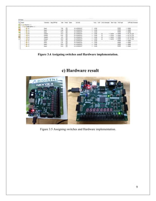
This project report describes the design, simulation, and implementation of a keypad scanner on an FPGA board. A Verilog code was written using a dataflow modeling style to scan a 3x4 keypad and output a 5-bit binary number corresponding to the pressed key. The code was simulated using Xilinx Vivado software. Finally, the design was implemented on a Digilent Nexys ddr FPGA board and tested successfully.
The project report on 'Keypad Scanner' is introduced by team members and faculty guidance. It outlines the report structure, including Abstract, Acknowledgement, Introduction, Implementation, Results, Conclusion, and References.
The abstract describes the keypad scanner project, which involves design, simulation, and implementation on FPGA using Verilog code and Xilinx Vivado software.
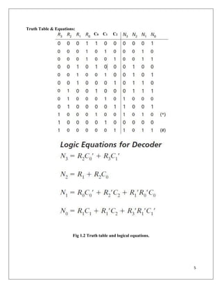
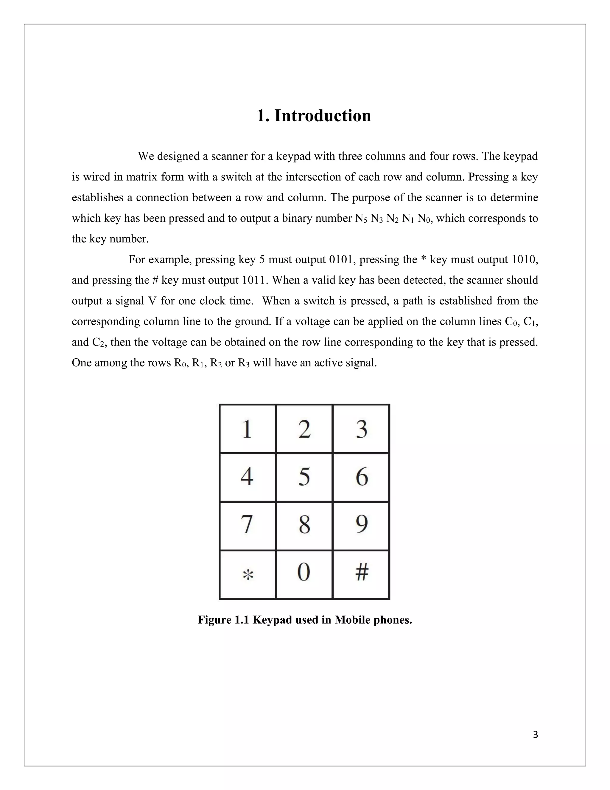
The introduction details the keypad's matrix design and function; pressed keys correspond to binary outputs. It summarizes the scanning procedure to detect keypress.
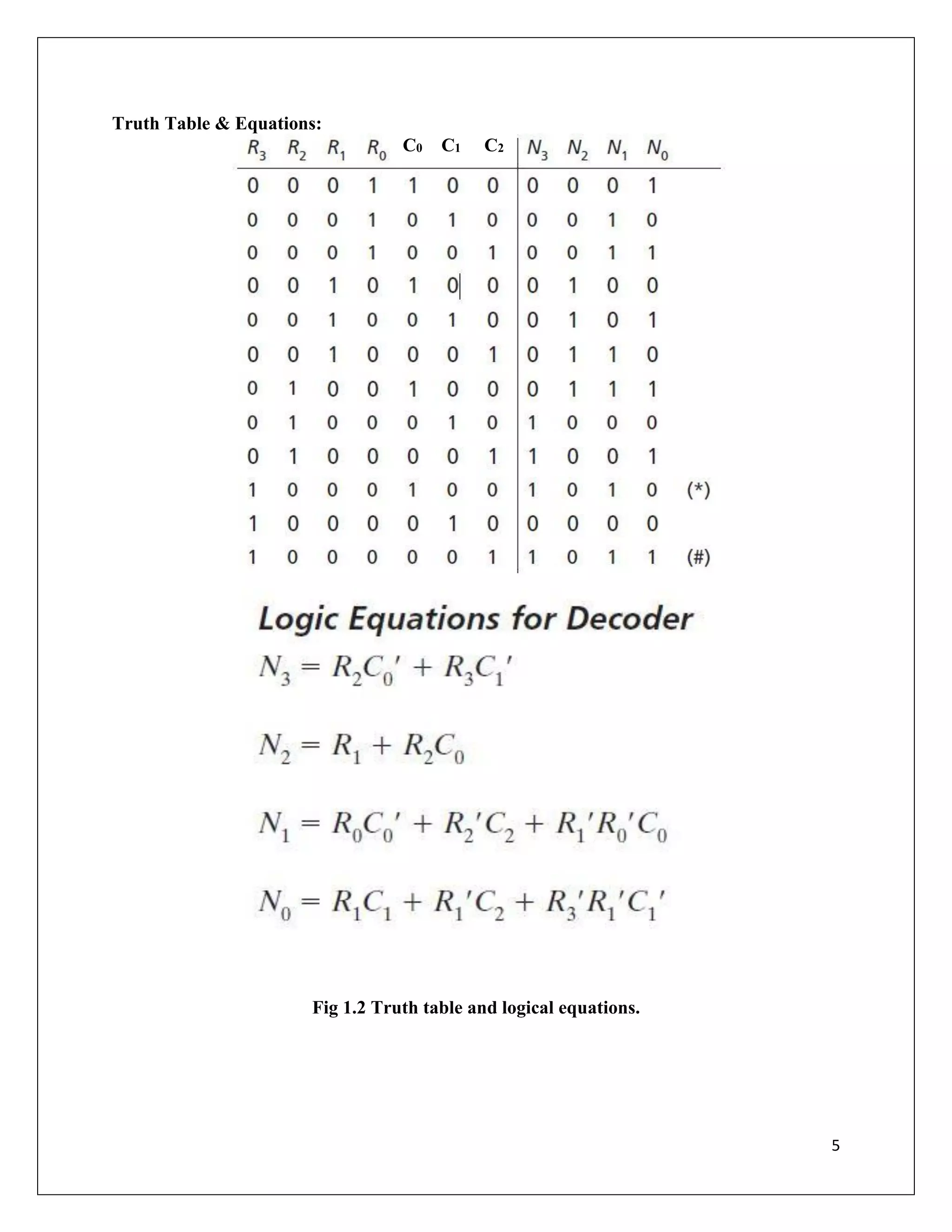
This section includes the truth table and logical equations for the keypad scanner, alongside the required software and hardware specifications for implementation.
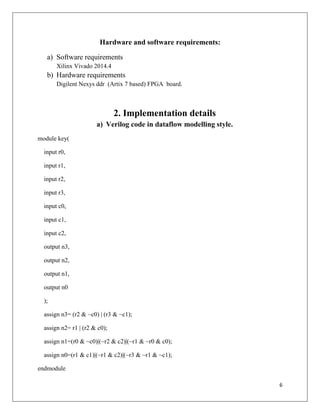
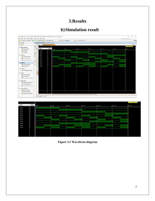
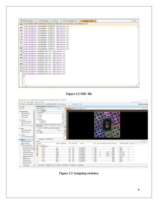
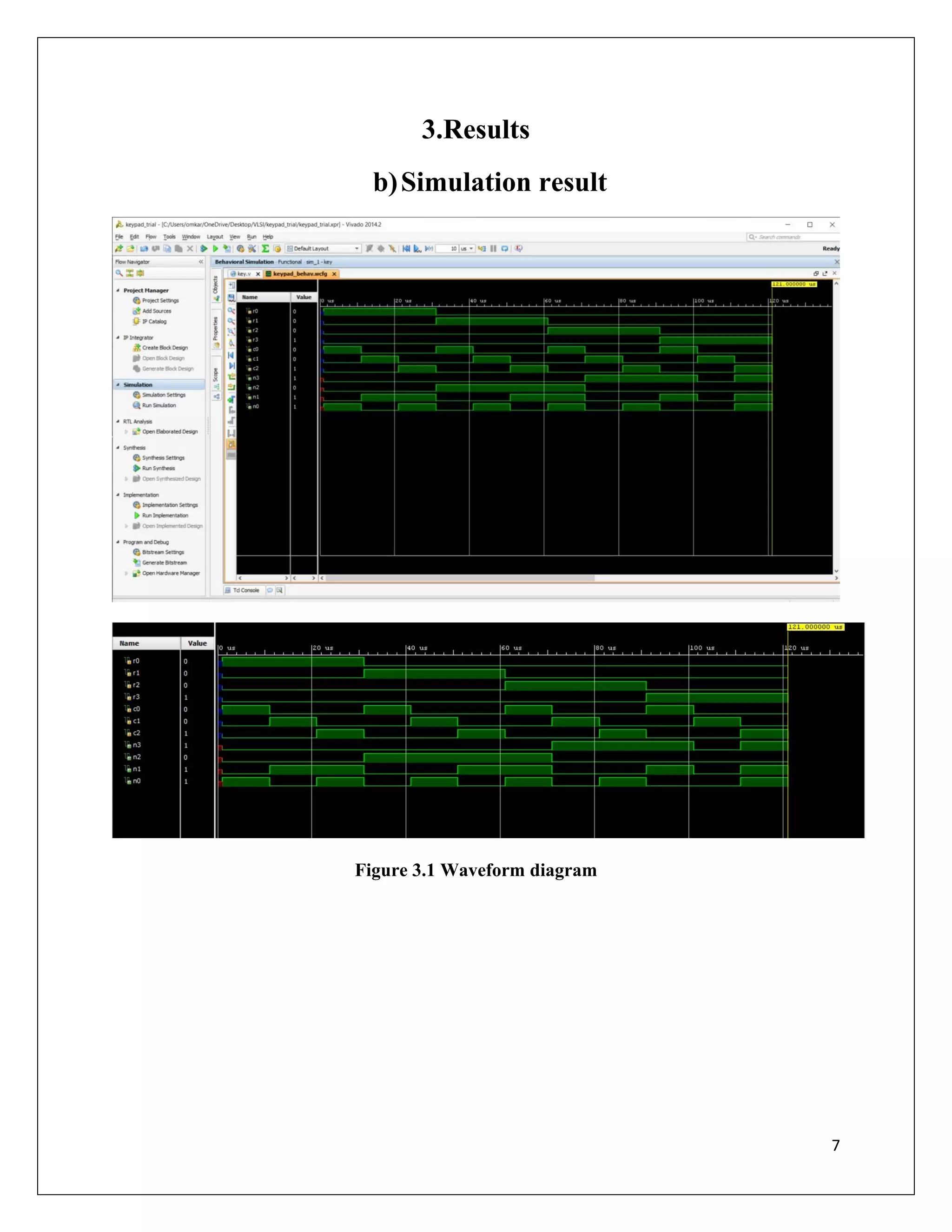
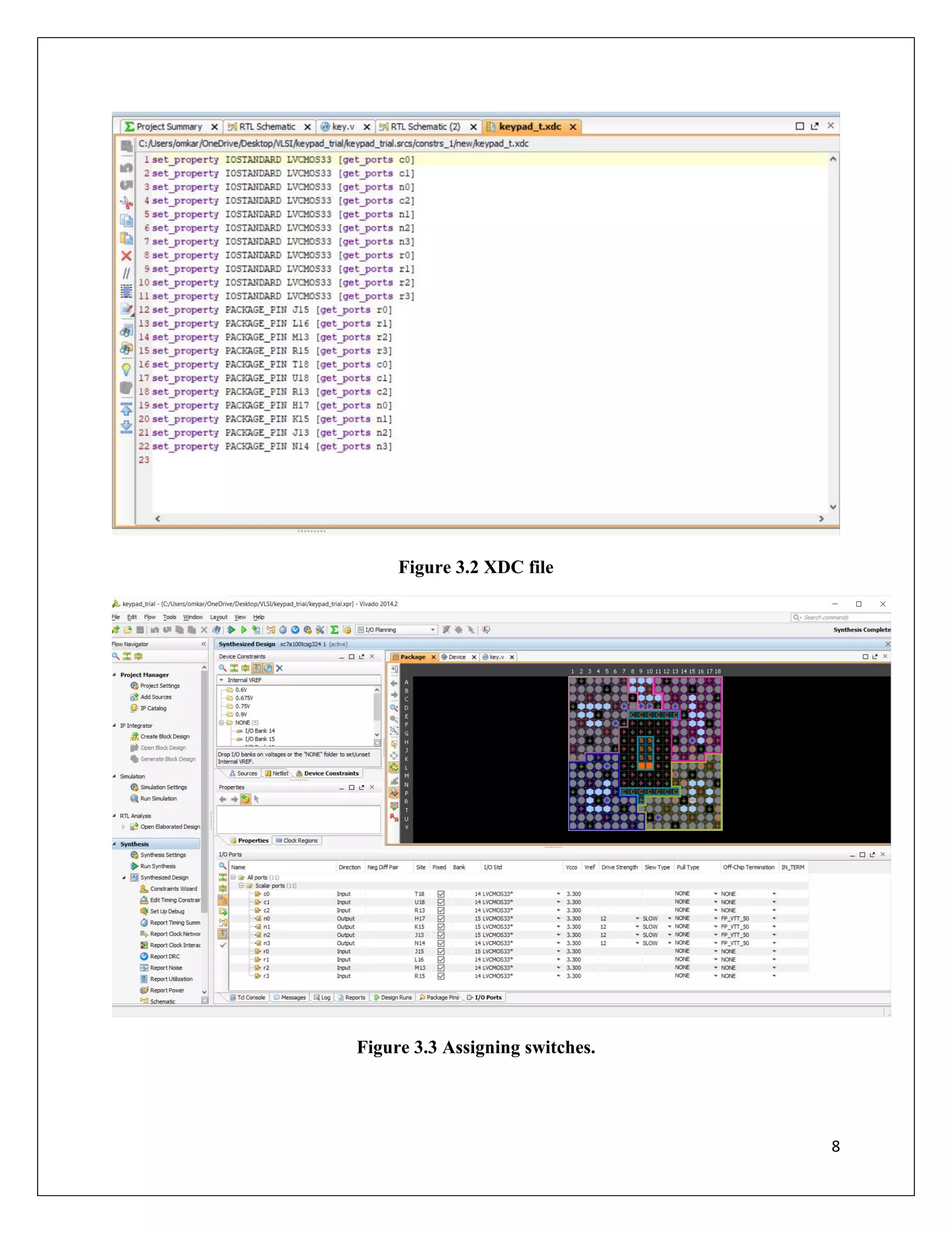
Results from simulations and hardware implementations are presented, along with corresponding figures showing waveforms and switch assignments, demonstrating successful functionality.
The conclusion confirms successful implementation and testing of the keypad scanner, highlighting the learning experience with logic programming on FPGA.
The references provide a list of important texts related to Verilog and digital design, contributing to the theoretical foundation of the project.


