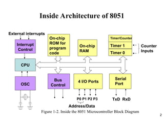
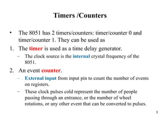
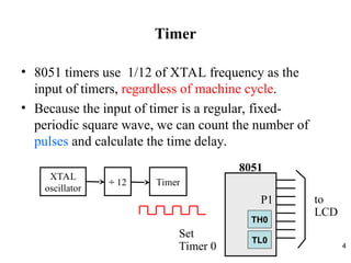
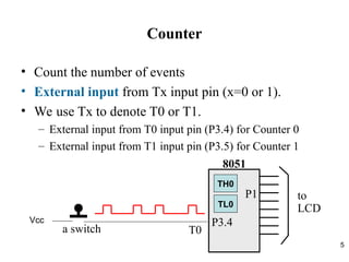
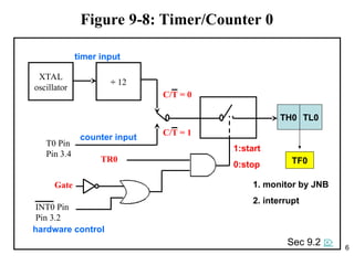
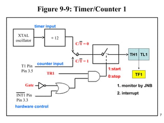
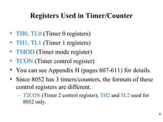
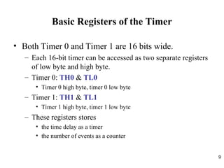
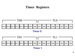
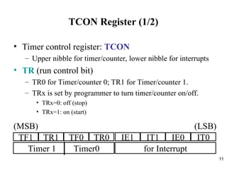
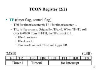
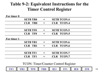
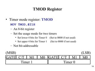
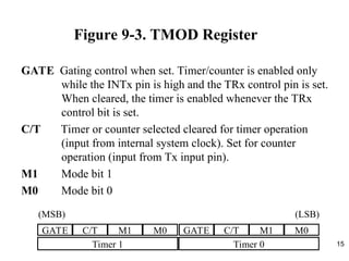
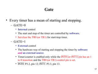
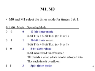
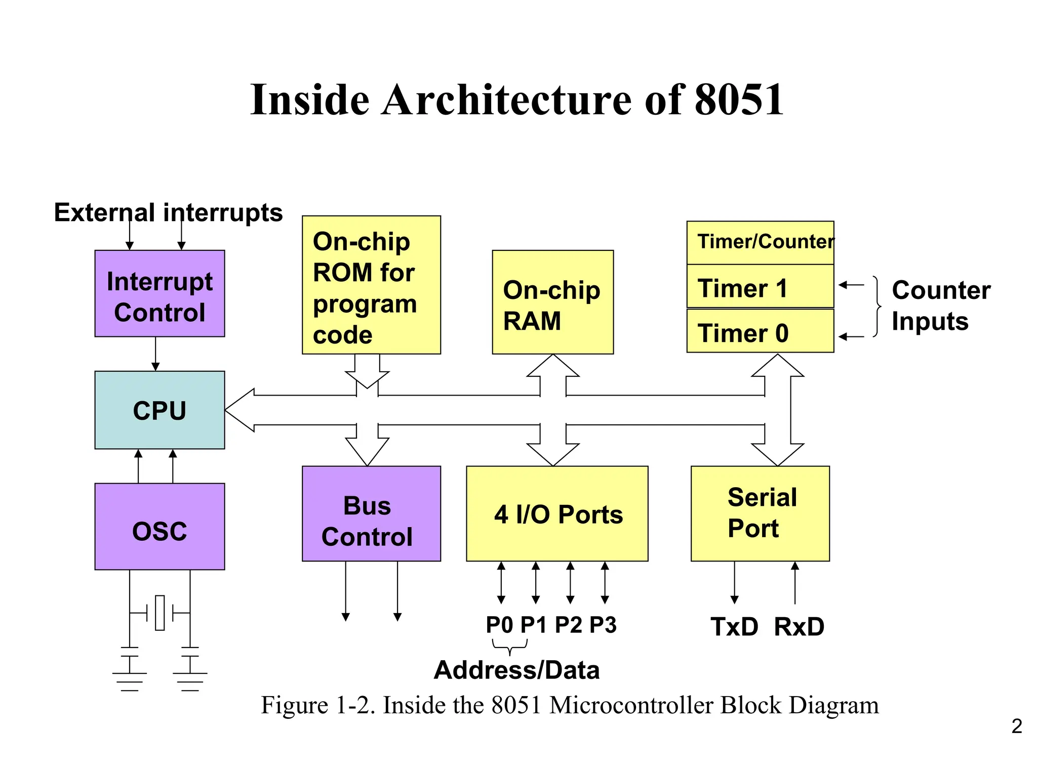
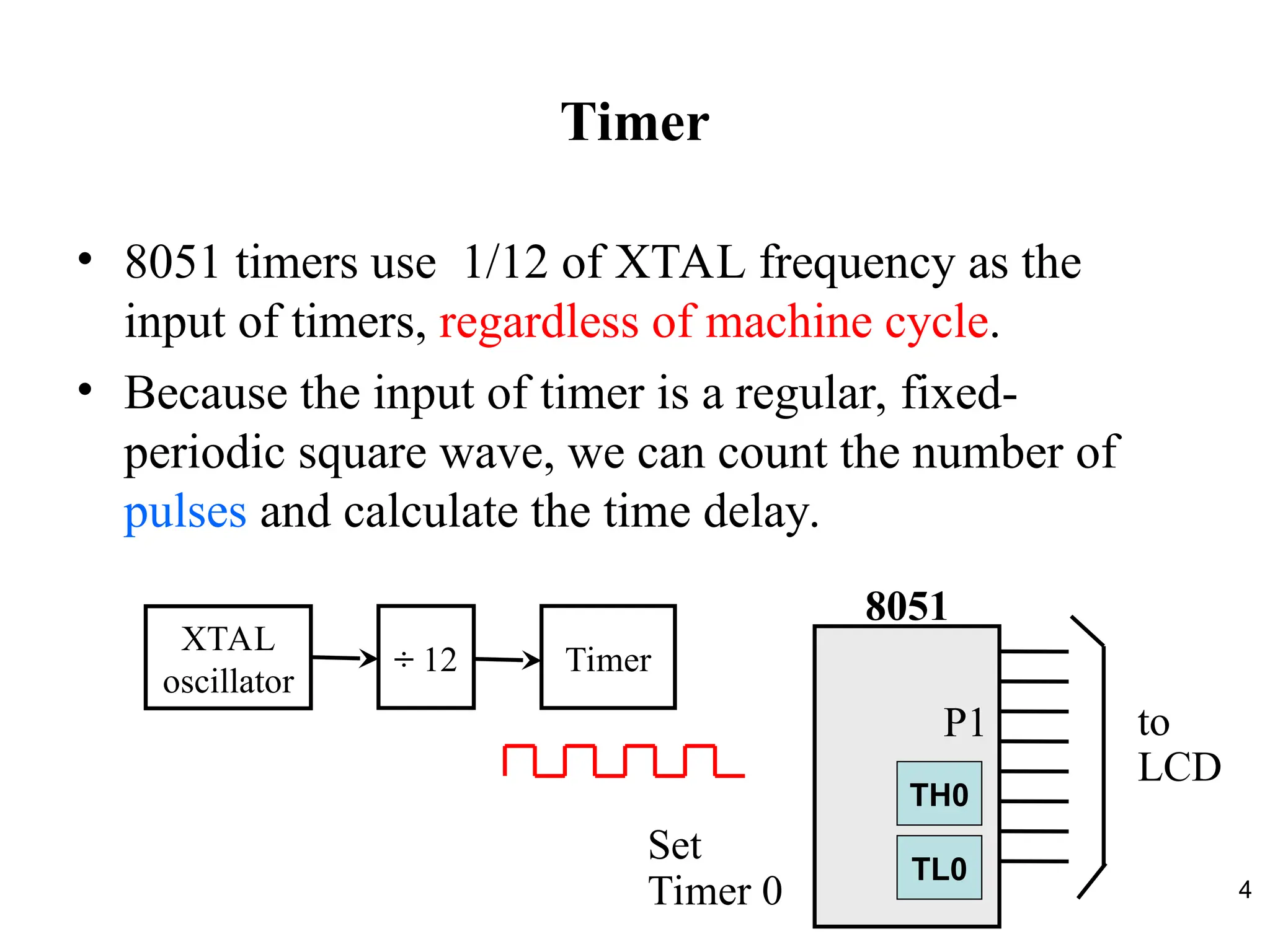
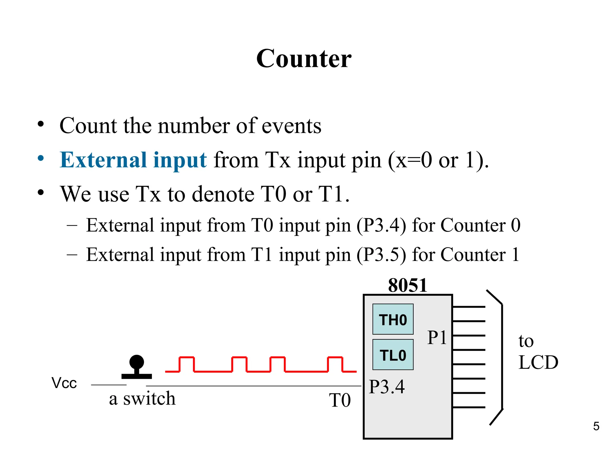
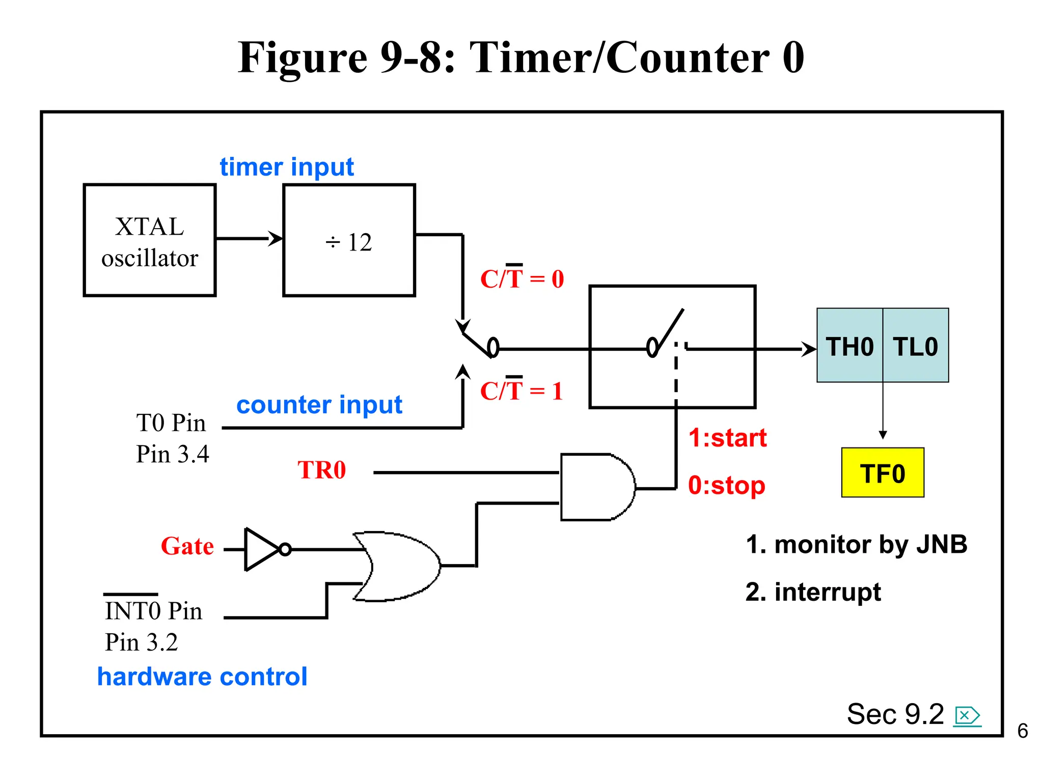
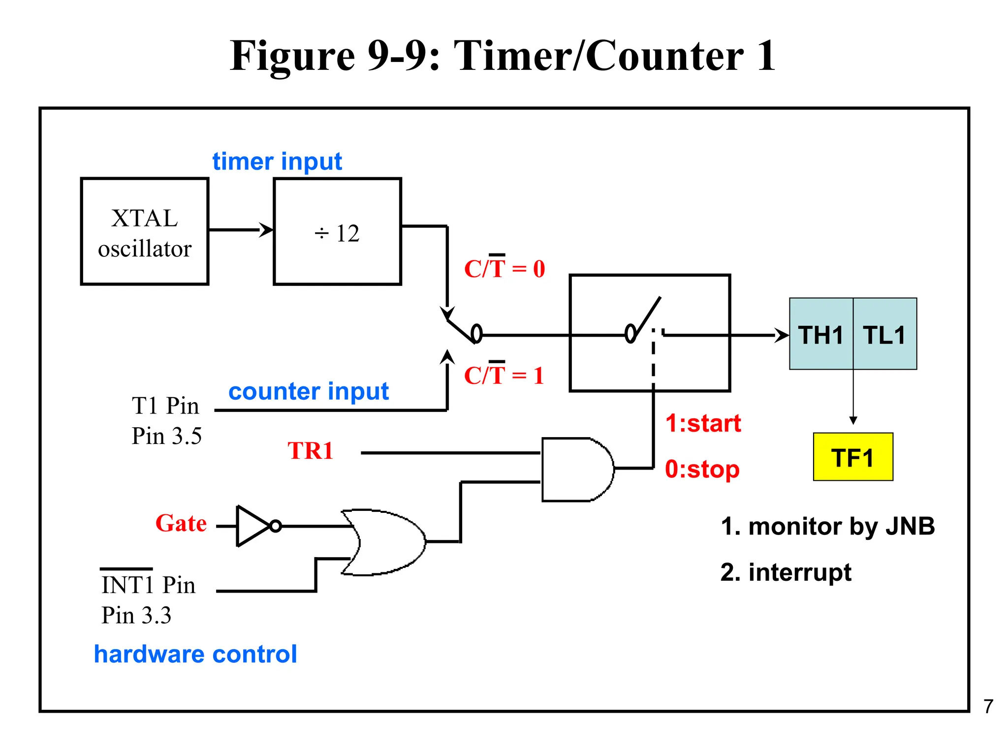
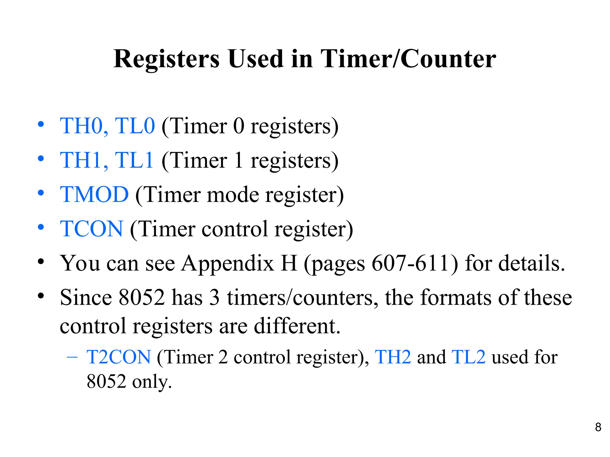
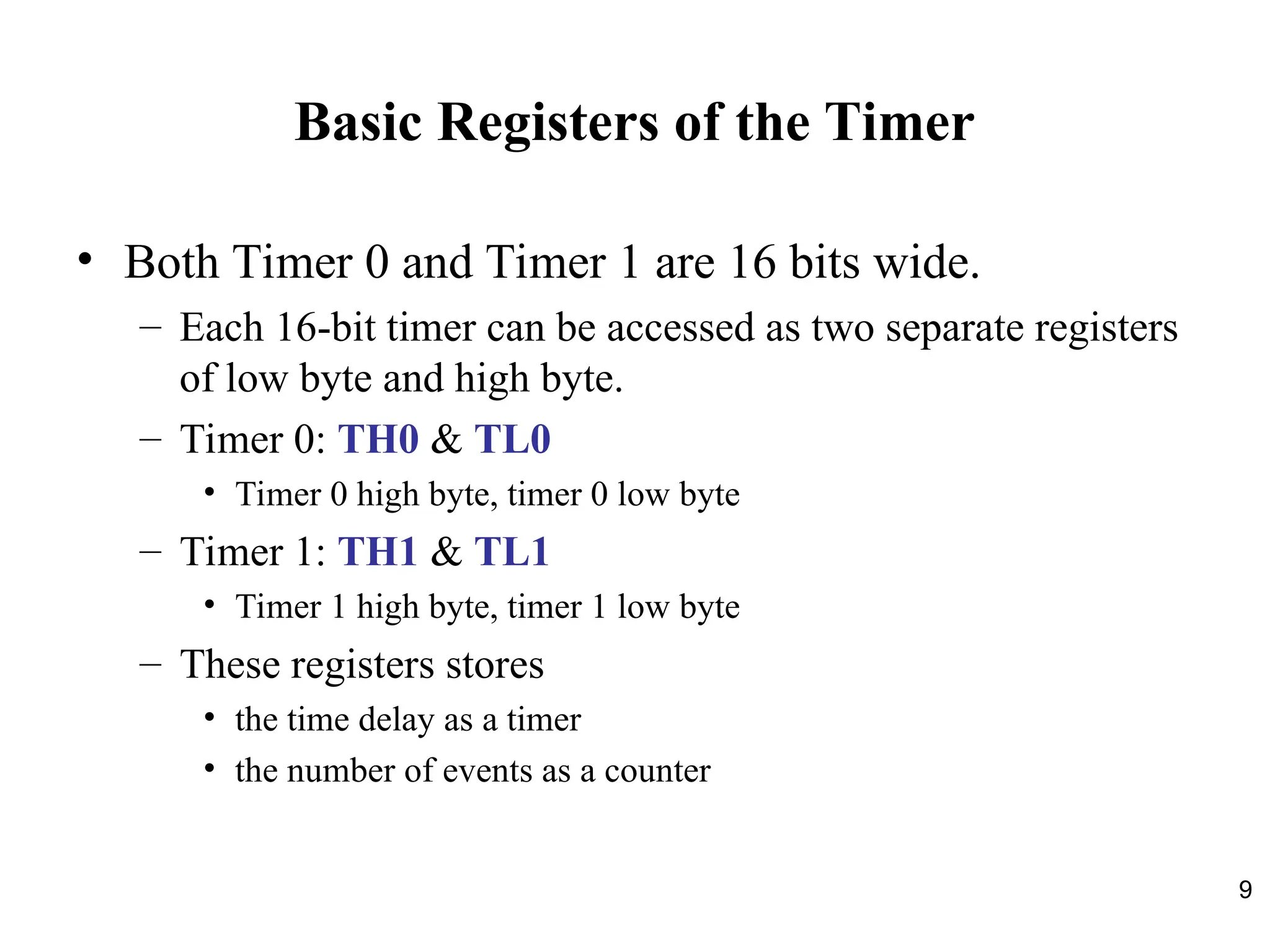
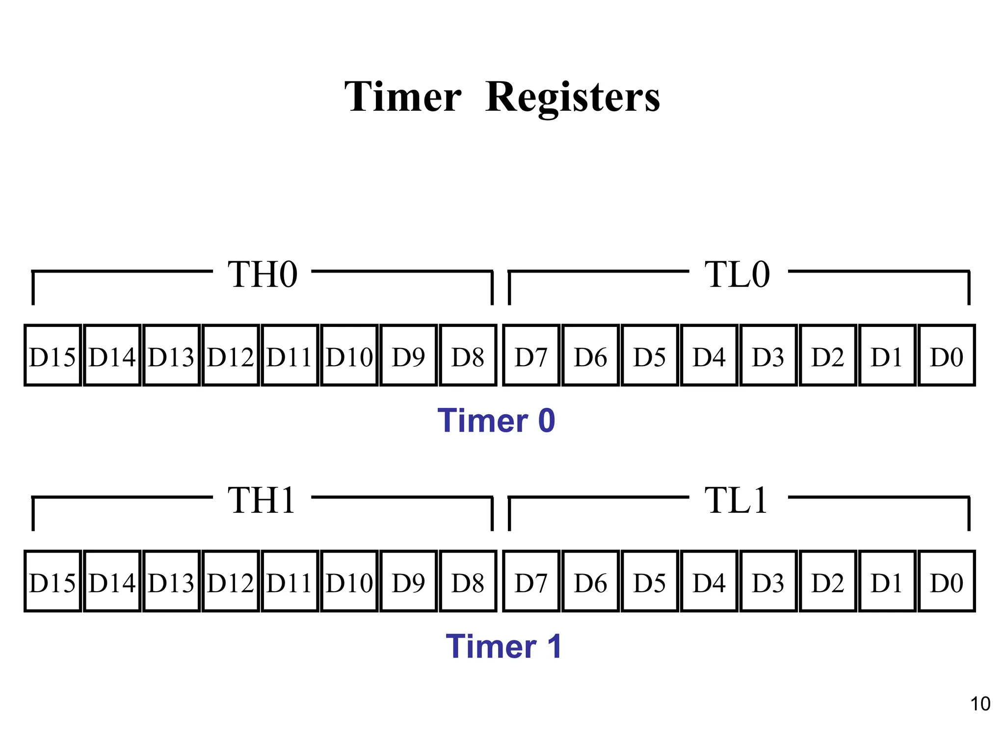
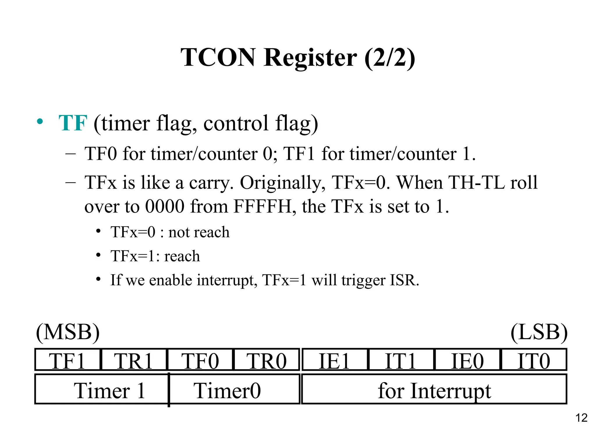
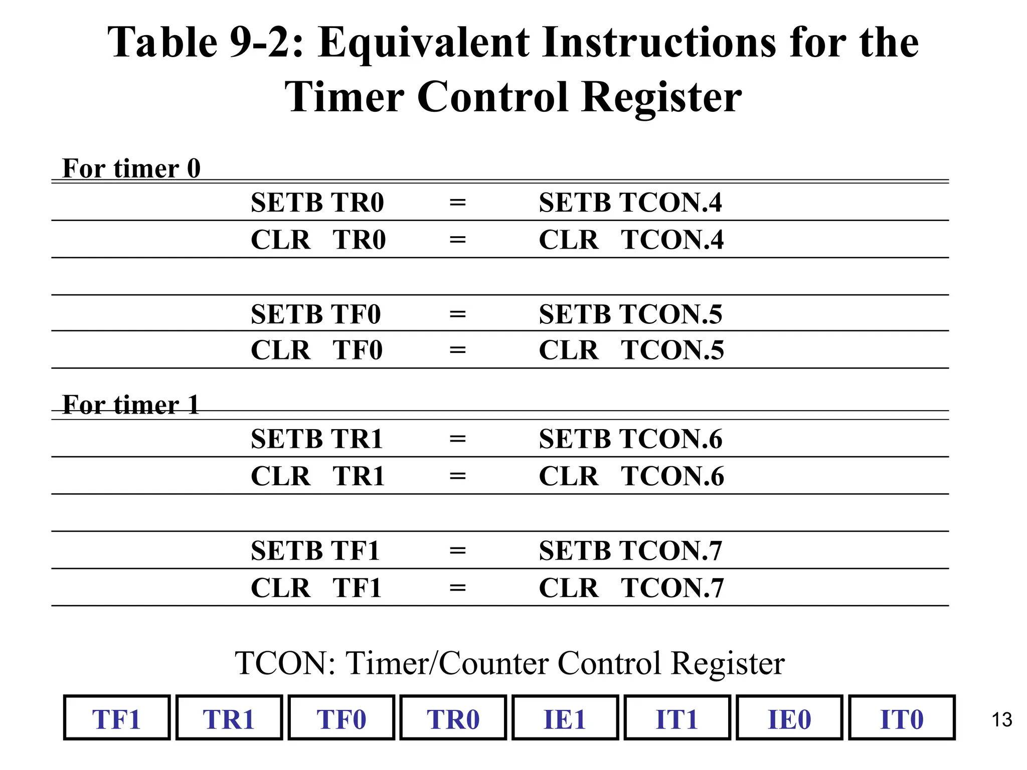
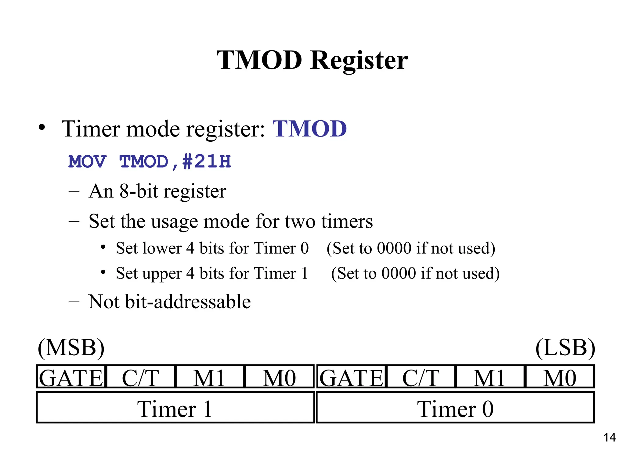
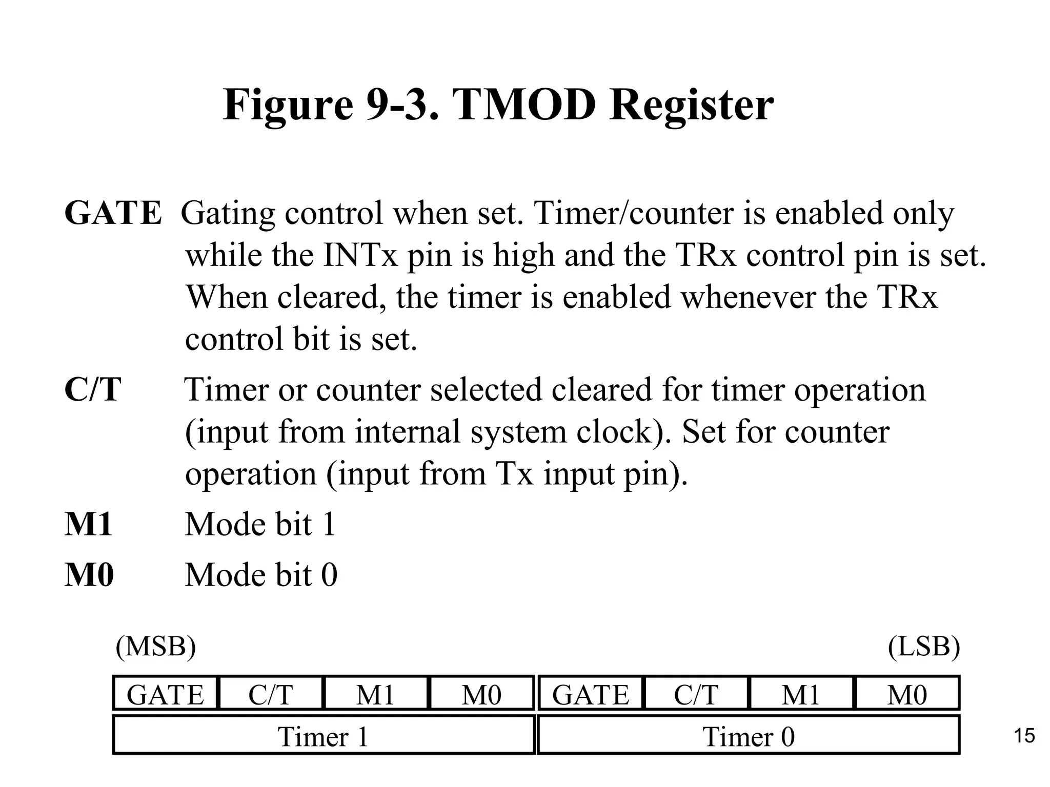
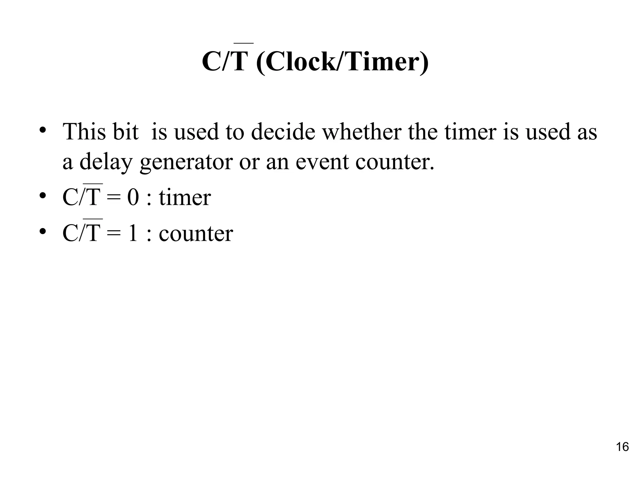
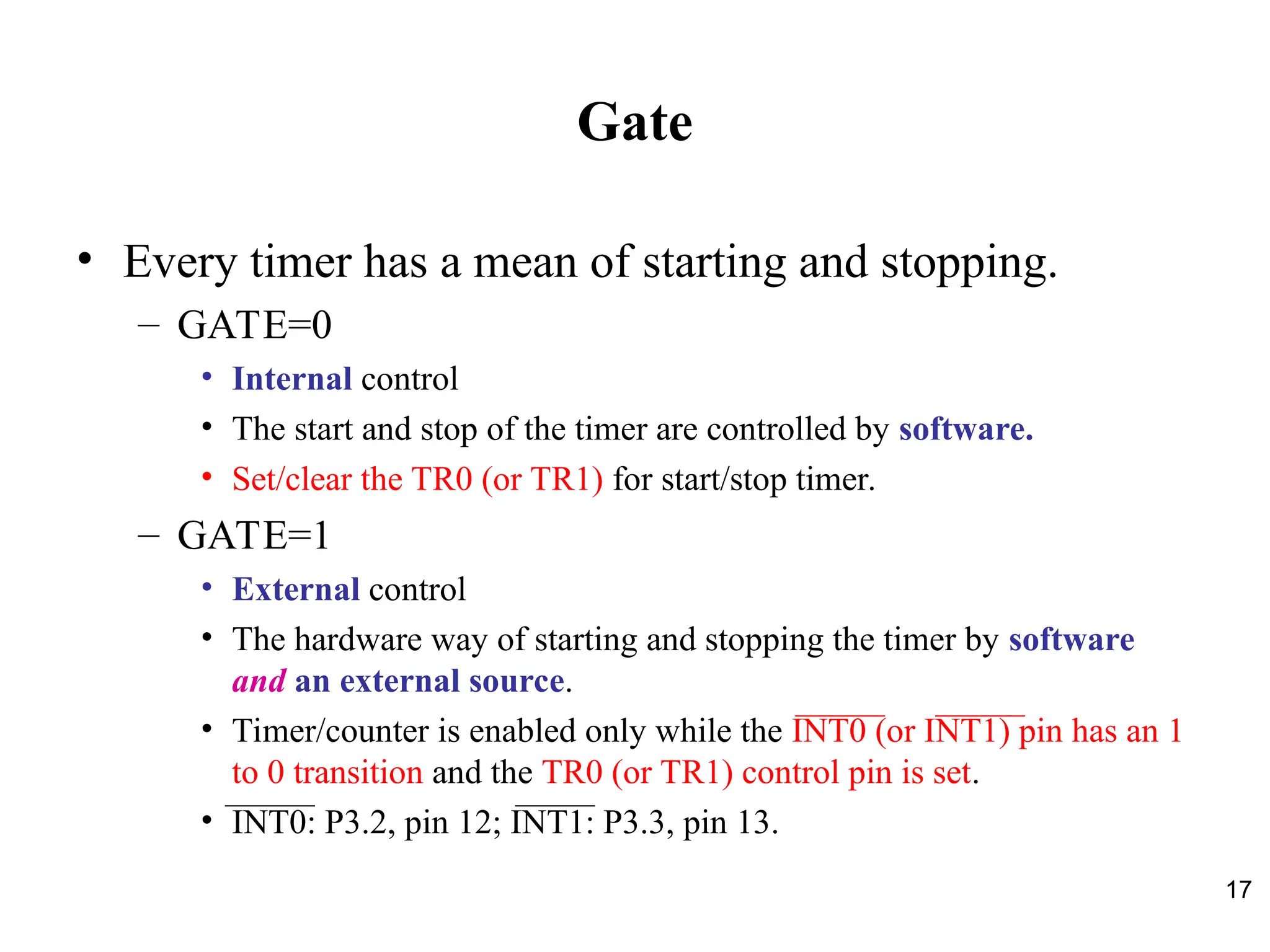
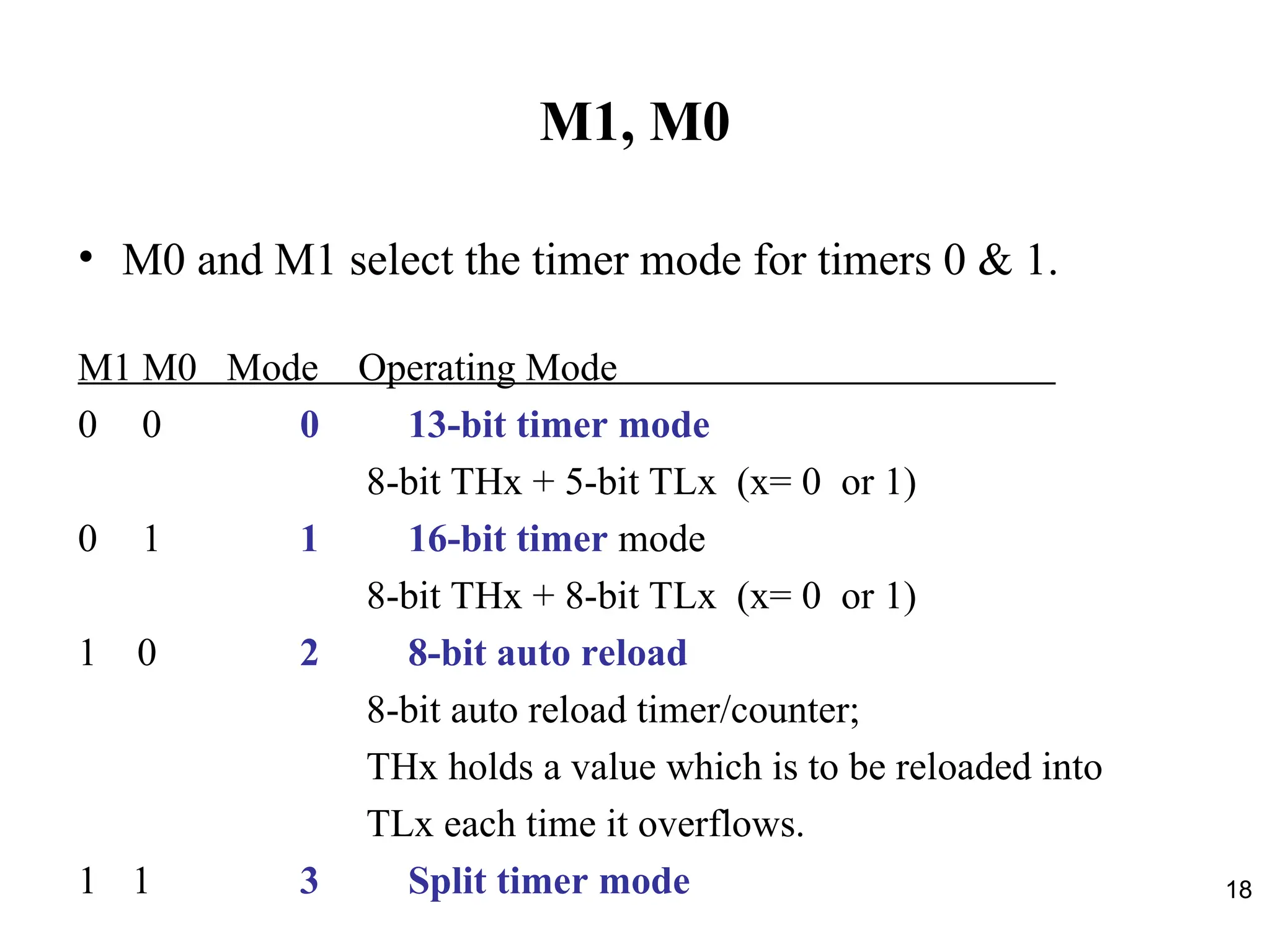
KEMBAR78
Microcontroller 8051 timer and counter module | PPT
1
8051 Timer Programming in
Assembly and C
Prepared By:
1400731090010
140073109012
140073109013
2
Inside Architecture of 8051
CPU
On-chip
RAM
On-chip
ROM for
program
code
4 I/O Ports
Timer 0
Serial
Port
Figure 1-2. Inside the 8051 Microcontroller Block Diagram
OSC
Interrupt
Control
External interrupts
Timer 1
Timer/Counter
Bus
Control
TxD RxD
P0 P1 P2 P3
Address/Data
Counter
Inputs
3
Timers /Counters
• The 8051 has 2 timers/counters: timer/counter 0 and
timer/counter 1. They can be used as
1. The timer is used as a time delay generator.
– The clock source is the internal crystal frequency of the
8051.
2. An event counter.
– External input from input pin to count the number of events
on registers.
– These clock pulses cold represent the number of people
passing through an entrance, or the number of wheel
rotations, or any other event that can be converted to pulses.
4
Timer
• 8051 timers use 1/12 of XTAL frequency as the
input of timers, regardless of machine cycle.
• Because the input of timer is a regular, fixed-
periodic square wave, we can count the number of
pulses and calculate the time delay.
to
LCD
P1
8051
TL0
TH0
Set
Timer 0
XTAL
oscillator
÷ 12 Timer
5
Counter
• Count the number of events
• External input from Tx input pin (x=0 or 1).
• We use Tx to denote T0 or T1.
– External input from T0 input pin (P3.4) for Counter 0
– External input from T1 input pin (P3.5) for Counter 1
T0
to
LCD
P3.4
P1
8051
a switch
TL0
TH0
Vcc
6
Figure 9-8: Timer/Counter 0
XTAL
oscillator
÷ 12
TR0
INT0 Pin
Pin 3.2
C/T = 0
Gate
T0 Pin
Pin 3.4
C/T = 1
TH0 TL0
TF0
1. monitor by JNB
2. interrupt
timer input
hardware control
1:start
0:stop
counter input
Sec 9.2 
7
Figure 9-9: Timer/Counter 1
XTAL
oscillator
÷ 12
TR1
INT1 Pin
Pin 3.3
C/T = 0
Gate
T1 Pin
Pin 3.5
C/T = 1
TH1 TL1
TF1
1. monitor by JNB
2. interrupt
1:start
0:stop
timer input
counter input
hardware control
8
Registers Used in Timer/Counter
• TH0, TL0 (Timer 0 registers)
• TH1, TL1 (Timer 1 registers)
• TMOD (Timer mode register)
• TCON (Timer control register)
• You can see Appendix H (pages 607-611) for details.
• Since 8052 has 3 timers/counters, the formats of these
control registers are different.
– T2CON (Timer 2 control register), TH2 and TL2 used for
8052 only.
9
Basic Registers of the Timer
• Both Timer 0 and Timer 1 are 16 bits wide.
– Each 16-bit timer can be accessed as two separate registers
of low byte and high byte.
– Timer 0: TH0 & TL0
• Timer 0 high byte, timer 0 low byte
– Timer 1: TH1 & TL1
• Timer 1 high byte, timer 1 low byte
– These registers stores
• the time delay as a timer
• the number of events as a counter
10
Timer Registers
D15 D8
D9
D10
D11
D12
D13
D14 D7 D0
D1
D2
D3
D4
D5
D6
TH0 TL0
D15 D8
D9
D10
D11
D12
D13
D14 D7 D0
D1
D2
D3
D4
D5
D6
TH1 TL1
Timer 0
Timer 1
11
TCON Register (1/2)
• Timer control register: TCON
– Upper nibble for timer/counter, lower nibble for interrupts
• TR (run control bit)
– TR0 for Timer/counter 0; TR1 for Timer/counter 1.
– TRx is set by programmer to turn timer/counter on/off.
• TRx=0: off (stop)
• TRx=1: on (start)
TF1 TR1 TF0 TR0 IE1 IT1 IE0 IT0
Timer 1 Timer0 for Interrupt
(MSB) (LSB)
12
TCON Register (2/2)
• TF (timer flag, control flag)
– TF0 for timer/counter 0; TF1 for timer/counter 1.
– TFx is like a carry. Originally, TFx=0. When TH-TL roll
over to 0000 from FFFFH, the TFx is set to 1.
• TFx=0 : not reach
• TFx=1: reach
• If we enable interrupt, TFx=1 will trigger ISR.
TF1 TR1 TF0 TR0 IE1 IT1 IE0 IT0
Timer 1 Timer0 for Interrupt
(MSB) (LSB)
13
Table 9-2: Equivalent Instructions for the
Timer Control Register
For timer 0
SETB TR0 = SETB TCON.4
CLR TR0 = CLR TCON.4
SETB TF0 = SETB TCON.5
CLR TF0 = CLR TCON.5
For timer 1
SETB TR1 = SETB TCON.6
CLR TR1 = CLR TCON.6
SETB TF1 = SETB TCON.7
CLR TF1 = CLR TCON.7
TF1 IT0
IE0
IT1
IE1
TR0
TF0
TR1
TCON: Timer/Counter Control Register
14
TMOD Register
• Timer mode register: TMOD
MOV TMOD,#21H
– An 8-bit register
– Set the usage mode for two timers
• Set lower 4 bits for Timer 0 (Set to 0000 if not used)
• Set upper 4 bits for Timer 1 (Set to 0000 if not used)
– Not bit-addressable
GATE C/T M1 M0 GATE C/T M1 M0
Timer 1 Timer 0
(MSB) (LSB)
15
Figure 9-3. TMOD Register
GATE Gating control when set. Timer/counter is enabled only
while the INTx pin is high and the TRx control pin is set.
When cleared, the timer is enabled whenever the TRx
control bit is set.
C/T Timer or counter selected cleared for timer operation
(input from internal system clock). Set for counter
operation (input from Tx input pin).
M1 Mode bit 1
M0 Mode bit 0
GATE C/T M1 M0 GATE C/T M1 M0
Timer 1 Timer 0
(MSB) (LSB)
16
C/T (Clock/Timer)
• This bit is used to decide whether the timer is used as
a delay generator or an event counter.
• C/T = 0 : timer
• C/T = 1 : counter
17
Gate
• Every timer has a mean of starting and stopping.
– GATE=0
• Internal control
• The start and stop of the timer are controlled by software.
• Set/clear the TR0 (or TR1) for start/stop timer.
– GATE=1
• External control
• The hardware way of starting and stopping the timer by software
and an external source.
• Timer/counter is enabled only while the INT0 (or INT1) pin has an 1
to 0 transition and the TR0 (or TR1) control pin is set.
• INT0: P3.2, pin 12; INT1: P3.3, pin 13.
18
M1, M0
• M0 and M1 select the timer mode for timers 0 & 1.
M1 M0 Mode Operating Mode
0 0 0 13-bit timer mode
8-bit THx + 5-bit TLx (x= 0 or 1)
0 1 1 16-bit timer mode
8-bit THx + 8-bit TLx (x= 0 or 1)
1 0 2 8-bit auto reload
8-bit auto reload timer/counter;
THx holds a value which is to be reloaded into
TLx each time it overflows.
1 1 3 Split timer mode
• THANK YOU
19

Microcontroller 8051 timer and counter module

  • 1.
    1 8051 Timer Programmingin Assembly and C Prepared By: 1400731090010 140073109012 140073109013
  • 2.
    2 Inside Architecture of8051 CPU On-chip RAM On-chip ROM for program code 4 I/O Ports Timer 0 Serial Port Figure 1-2. Inside the 8051 Microcontroller Block Diagram OSC Interrupt Control External interrupts Timer 1 Timer/Counter Bus Control TxD RxD P0 P1 P2 P3 Address/Data Counter Inputs
  • 3.
    3 Timers /Counters • The8051 has 2 timers/counters: timer/counter 0 and timer/counter 1. They can be used as 1. The timer is used as a time delay generator. – The clock source is the internal crystal frequency of the 8051. 2. An event counter. – External input from input pin to count the number of events on registers. – These clock pulses cold represent the number of people passing through an entrance, or the number of wheel rotations, or any other event that can be converted to pulses.
  • 4.
    4 Timer • 8051 timersuse 1/12 of XTAL frequency as the input of timers, regardless of machine cycle. • Because the input of timer is a regular, fixed- periodic square wave, we can count the number of pulses and calculate the time delay. to LCD P1 8051 TL0 TH0 Set Timer 0 XTAL oscillator ÷ 12 Timer
  • 5.
    5 Counter • Count thenumber of events • External input from Tx input pin (x=0 or 1). • We use Tx to denote T0 or T1. – External input from T0 input pin (P3.4) for Counter 0 – External input from T1 input pin (P3.5) for Counter 1 T0 to LCD P3.4 P1 8051 a switch TL0 TH0 Vcc
  • 6.
    6 Figure 9-8: Timer/Counter0 XTAL oscillator ÷ 12 TR0 INT0 Pin Pin 3.2 C/T = 0 Gate T0 Pin Pin 3.4 C/T = 1 TH0 TL0 TF0 1. monitor by JNB 2. interrupt timer input hardware control 1:start 0:stop counter input Sec 9.2 
  • 7.
    7 Figure 9-9: Timer/Counter1 XTAL oscillator ÷ 12 TR1 INT1 Pin Pin 3.3 C/T = 0 Gate T1 Pin Pin 3.5 C/T = 1 TH1 TL1 TF1 1. monitor by JNB 2. interrupt 1:start 0:stop timer input counter input hardware control
  • 8.
    8 Registers Used inTimer/Counter • TH0, TL0 (Timer 0 registers) • TH1, TL1 (Timer 1 registers) • TMOD (Timer mode register) • TCON (Timer control register) • You can see Appendix H (pages 607-611) for details. • Since 8052 has 3 timers/counters, the formats of these control registers are different. – T2CON (Timer 2 control register), TH2 and TL2 used for 8052 only.
  • 9.
    9 Basic Registers ofthe Timer • Both Timer 0 and Timer 1 are 16 bits wide. – Each 16-bit timer can be accessed as two separate registers of low byte and high byte. – Timer 0: TH0 & TL0 • Timer 0 high byte, timer 0 low byte – Timer 1: TH1 & TL1 • Timer 1 high byte, timer 1 low byte – These registers stores • the time delay as a timer • the number of events as a counter
  • 10.
    10 Timer Registers D15 D8 D9 D10 D11 D12 D13 D14D7 D0 D1 D2 D3 D4 D5 D6 TH0 TL0 D15 D8 D9 D10 D11 D12 D13 D14 D7 D0 D1 D2 D3 D4 D5 D6 TH1 TL1 Timer 0 Timer 1
  • 11.
    11 TCON Register (1/2) •Timer control register: TCON – Upper nibble for timer/counter, lower nibble for interrupts • TR (run control bit) – TR0 for Timer/counter 0; TR1 for Timer/counter 1. – TRx is set by programmer to turn timer/counter on/off. • TRx=0: off (stop) • TRx=1: on (start) TF1 TR1 TF0 TR0 IE1 IT1 IE0 IT0 Timer 1 Timer0 for Interrupt (MSB) (LSB)
  • 12.
    12 TCON Register (2/2) •TF (timer flag, control flag) – TF0 for timer/counter 0; TF1 for timer/counter 1. – TFx is like a carry. Originally, TFx=0. When TH-TL roll over to 0000 from FFFFH, the TFx is set to 1. • TFx=0 : not reach • TFx=1: reach • If we enable interrupt, TFx=1 will trigger ISR. TF1 TR1 TF0 TR0 IE1 IT1 IE0 IT0 Timer 1 Timer0 for Interrupt (MSB) (LSB)
  • 13.
    13 Table 9-2: EquivalentInstructions for the Timer Control Register For timer 0 SETB TR0 = SETB TCON.4 CLR TR0 = CLR TCON.4 SETB TF0 = SETB TCON.5 CLR TF0 = CLR TCON.5 For timer 1 SETB TR1 = SETB TCON.6 CLR TR1 = CLR TCON.6 SETB TF1 = SETB TCON.7 CLR TF1 = CLR TCON.7 TF1 IT0 IE0 IT1 IE1 TR0 TF0 TR1 TCON: Timer/Counter Control Register
  • 14.
    14 TMOD Register • Timermode register: TMOD MOV TMOD,#21H – An 8-bit register – Set the usage mode for two timers • Set lower 4 bits for Timer 0 (Set to 0000 if not used) • Set upper 4 bits for Timer 1 (Set to 0000 if not used) – Not bit-addressable GATE C/T M1 M0 GATE C/T M1 M0 Timer 1 Timer 0 (MSB) (LSB)
  • 15.
    15 Figure 9-3. TMODRegister GATE Gating control when set. Timer/counter is enabled only while the INTx pin is high and the TRx control pin is set. When cleared, the timer is enabled whenever the TRx control bit is set. C/T Timer or counter selected cleared for timer operation (input from internal system clock). Set for counter operation (input from Tx input pin). M1 Mode bit 1 M0 Mode bit 0 GATE C/T M1 M0 GATE C/T M1 M0 Timer 1 Timer 0 (MSB) (LSB)
  • 16.
    16 C/T (Clock/Timer) • Thisbit is used to decide whether the timer is used as a delay generator or an event counter. • C/T = 0 : timer • C/T = 1 : counter
  • 17.
    17 Gate • Every timerhas a mean of starting and stopping. – GATE=0 • Internal control • The start and stop of the timer are controlled by software. • Set/clear the TR0 (or TR1) for start/stop timer. – GATE=1 • External control • The hardware way of starting and stopping the timer by software and an external source. • Timer/counter is enabled only while the INT0 (or INT1) pin has an 1 to 0 transition and the TR0 (or TR1) control pin is set. • INT0: P3.2, pin 12; INT1: P3.3, pin 13.
  • 18.
    18 M1, M0 • M0and M1 select the timer mode for timers 0 & 1. M1 M0 Mode Operating Mode 0 0 0 13-bit timer mode 8-bit THx + 5-bit TLx (x= 0 or 1) 0 1 1 16-bit timer mode 8-bit THx + 8-bit TLx (x= 0 or 1) 1 0 2 8-bit auto reload 8-bit auto reload timer/counter; THx holds a value which is to be reloaded into TLx each time it overflows. 1 1 3 Split timer mode
  • 19.

Editor's Notes

  • #2 再三強調 timer/counter 是兩個獨立於 CPU 之外的硬體, 有自己的線路與運作, 但 CPU 要控制它們, 以達到目的.
  • #17 GATE=0 表示只要 TR0/TR1 被設成 1, timer/counter 就會開始運作. GATE=1 表示除了 TR0/TR1 要被設成 1 之外, INT0/INT1 也要被設成0, timer/counter 就會開始運作. the 1 to 0 transition on INT0 (P3.2)
  • #18 在mode 3 中, counter/timer 0 的 TL0 為 8 bit 的 timer/counter; TH0 為 8 bit 的 timer. 至於 Timer/counter 1 則停止動作.