Downloaded 421 times


![• A maskable interrupt can be enabled or disabled by
executing instruction such as EI and DI.
• If the μP’s interrupt is disabled , the μcomputer
ignores a maskable interrupt.
• Interrupt flag- [ 1 – maskable interrupt are diabled]
• The non maskable interrupt has the higher priority
over the maskable iterrupt and cannot be enabled and
disabled by instructions.
• If both maskable interrupt and the non maskable
interrupt are activated at same time,the priority will
goes to …………………….](https://image.slidesharecdn.com/iooperations-141101091256-conversion-gate02/85/MICROPROCESSOR-INPUT-OUTPUT-OPERATIONS-15-320.jpg)


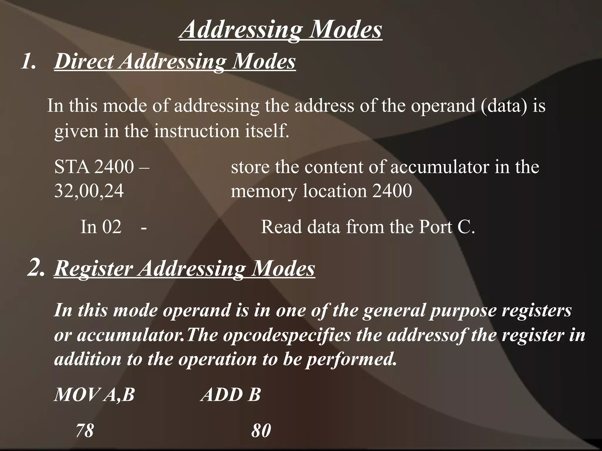
![3. Register Indirect Addressing
In this mode the address of the operand is specified by the
register pair.
LXI H, 2500 load H-L pair with 2500
MOV A,M move the content of the memory location,
whose address is in the H-L pair to the
accumulator.
[MOV A,M – is an example for Register Indirect
Addressing Mode]
LXI H, 2500
ADD M
HLT](https://image.slidesharecdn.com/iooperations-141101091256-conversion-gate02/85/MICROPROCESSOR-INPUT-OUTPUT-OPERATIONS-26-320.jpg)
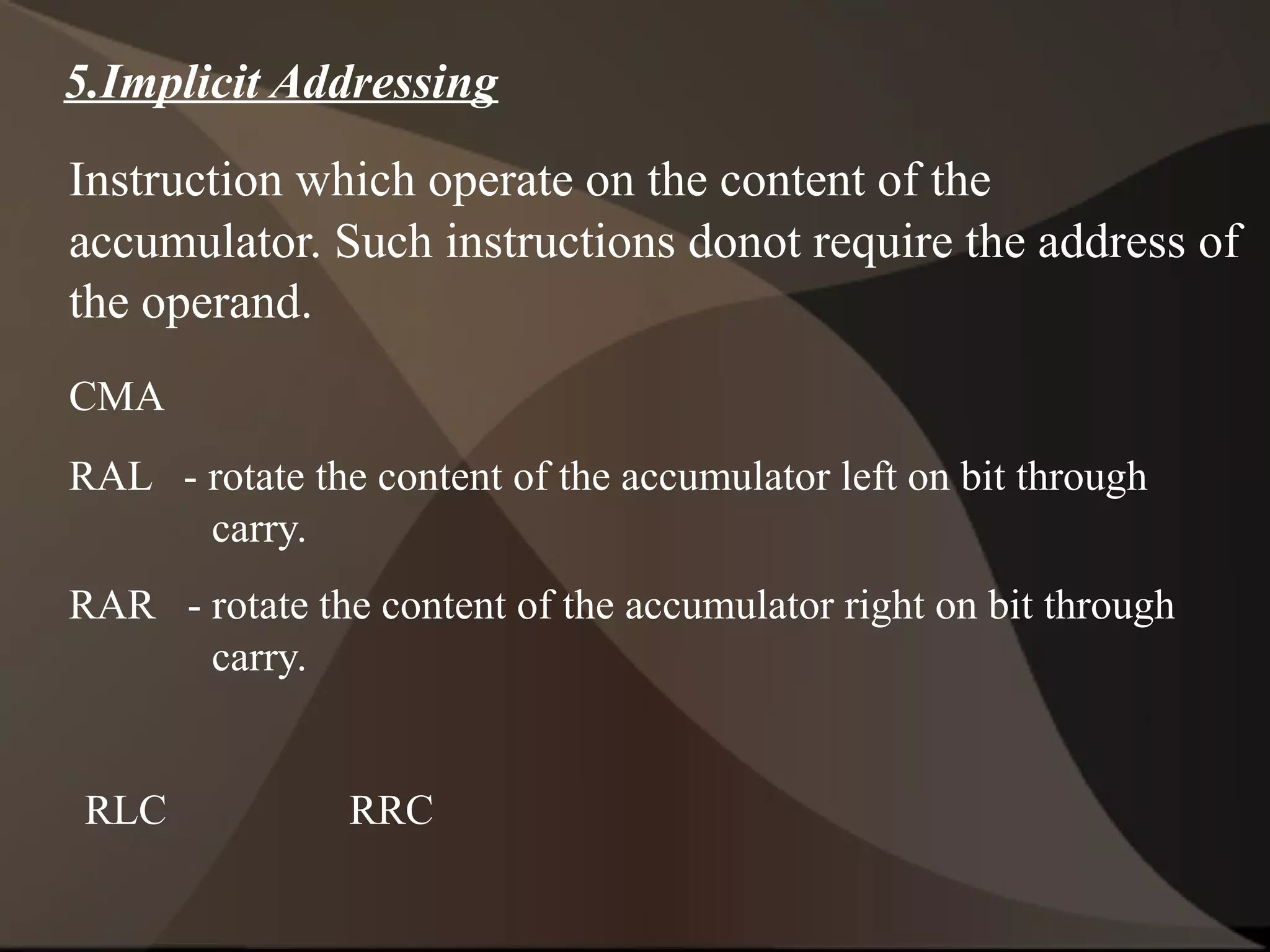
![4. Immediate Addressing Mode
In immediate addressing mode the operand is specified
with in the instruction itself.
MVI A,05
[3E, 05] ----------- code form
ADI 06
[C6, 06]
In the instructions the 2nd byte specifies data.](https://image.slidesharecdn.com/iooperations-141101091256-conversion-gate02/85/MICROPROCESSOR-INPUT-OUTPUT-OPERATIONS-27-320.jpg)
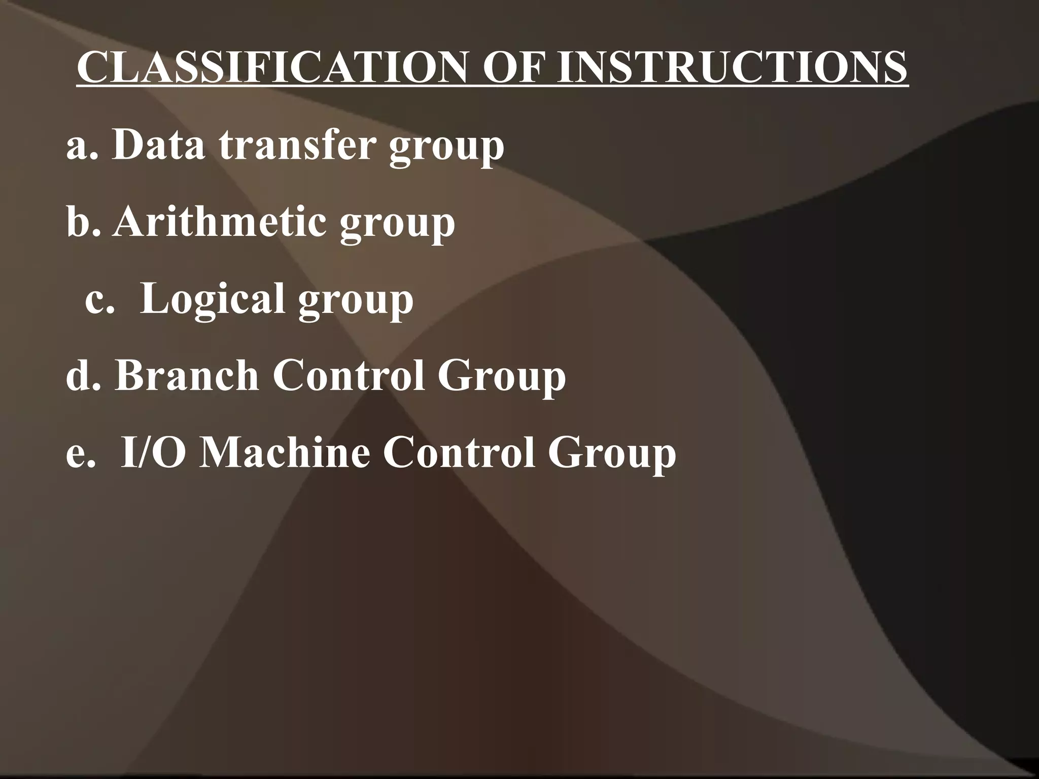
![b. Arithmetic Group
• The instruction under arithmetic group perform
arithmetic operation such as addition, subtraction,
increment, decrement of the content of a register or
memory.
ADD r
ADD M
ADC r [A] [A] + [r] + [CS]
ADC M
ADI - add immediate data to accumulator
DAD rp [H-L] [H-L] + [rp]
SUB r SUB M INR r INR M](https://image.slidesharecdn.com/iooperations-141101091256-conversion-gate02/85/MICROPROCESSOR-INPUT-OUTPUT-OPERATIONS-32-320.jpg)


![• A maskable interrupt can be enabled or disabled by
executing instruction such as EI and DI.
• If the μP’s interrupt is disabled , the μcomputer
ignores a maskable interrupt.
• Interrupt flag- [ 1 – maskable interrupt are diabled]
• The non maskable interrupt has the higher priority
over the maskable iterrupt and cannot be enabled and
disabled by instructions.
• If both maskable interrupt and the non maskable
interrupt are activated at same time,the priority will
goes to …………………….](https://image.slidesharecdn.com/iooperations-141101091256-conversion-gate02/75/MICROPROCESSOR-INPUT-OUTPUT-OPERATIONS-15-2048.jpg)

![3. Register Indirect Addressing
In this mode the address of the operand is specified by the
register pair.
LXI H, 2500 load H-L pair with 2500
MOV A,M move the content of the memory location,
whose address is in the H-L pair to the
accumulator.
[MOV A,M – is an example for Register Indirect
Addressing Mode]
LXI H, 2500
ADD M
HLT](https://image.slidesharecdn.com/iooperations-141101091256-conversion-gate02/75/MICROPROCESSOR-INPUT-OUTPUT-OPERATIONS-26-2048.jpg)
![4. Immediate Addressing Mode
In immediate addressing mode the operand is specified
with in the instruction itself.
MVI A,05
[3E, 05] ----------- code form
ADI 06
[C6, 06]
In the instructions the 2nd byte specifies data.](https://image.slidesharecdn.com/iooperations-141101091256-conversion-gate02/75/MICROPROCESSOR-INPUT-OUTPUT-OPERATIONS-27-2048.jpg)
![b. Arithmetic Group
• The instruction under arithmetic group perform
arithmetic operation such as addition, subtraction,
increment, decrement of the content of a register or
memory.
ADD r
ADD M
ADC r [A] [A] + [r] + [CS]
ADC M
ADI - add immediate data to accumulator
DAD rp [H-L] [H-L] + [rp]
SUB r SUB M INR r INR M](https://image.slidesharecdn.com/iooperations-141101091256-conversion-gate02/75/MICROPROCESSOR-INPUT-OUTPUT-OPERATIONS-32-2048.jpg)


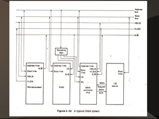
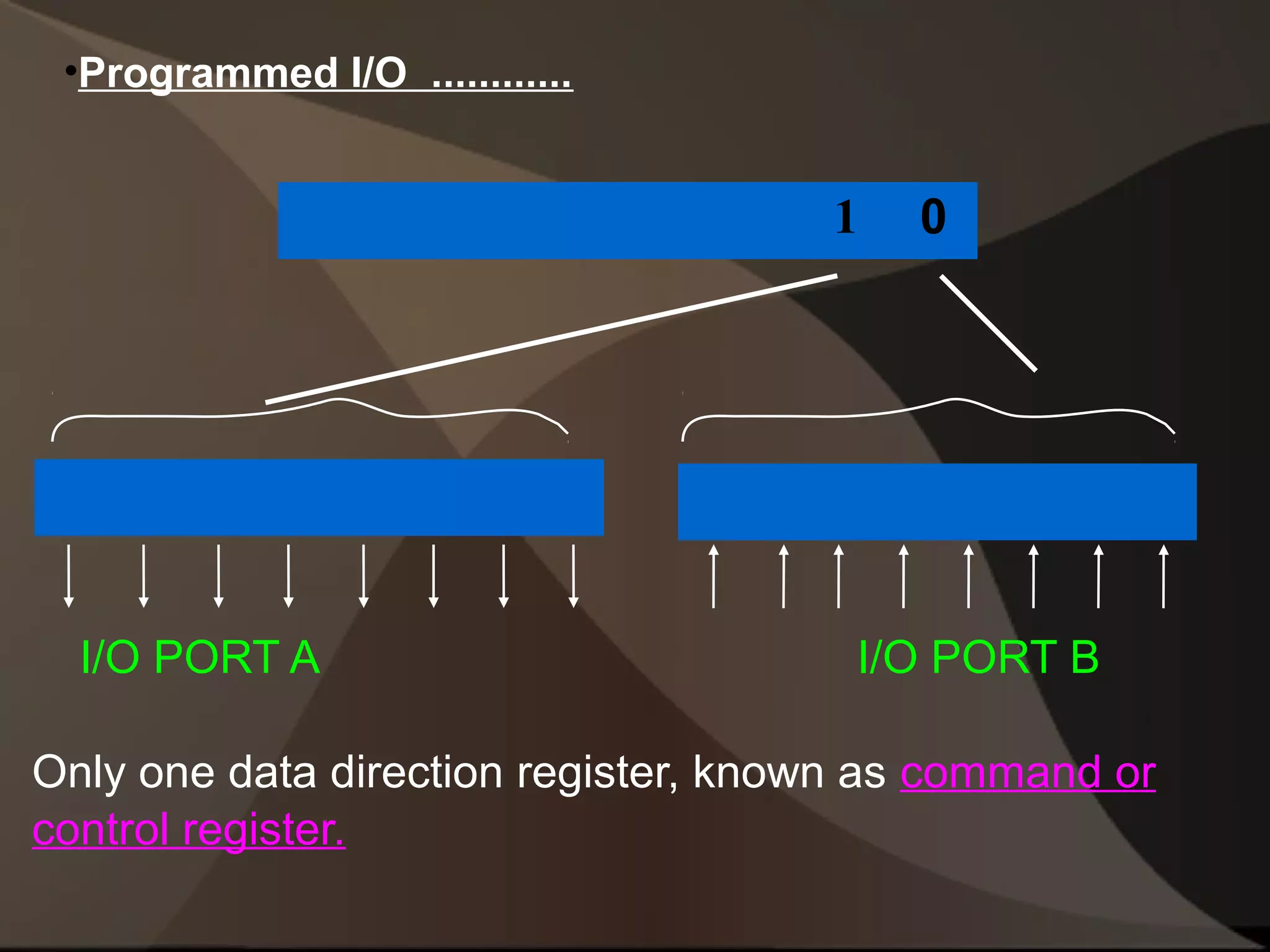
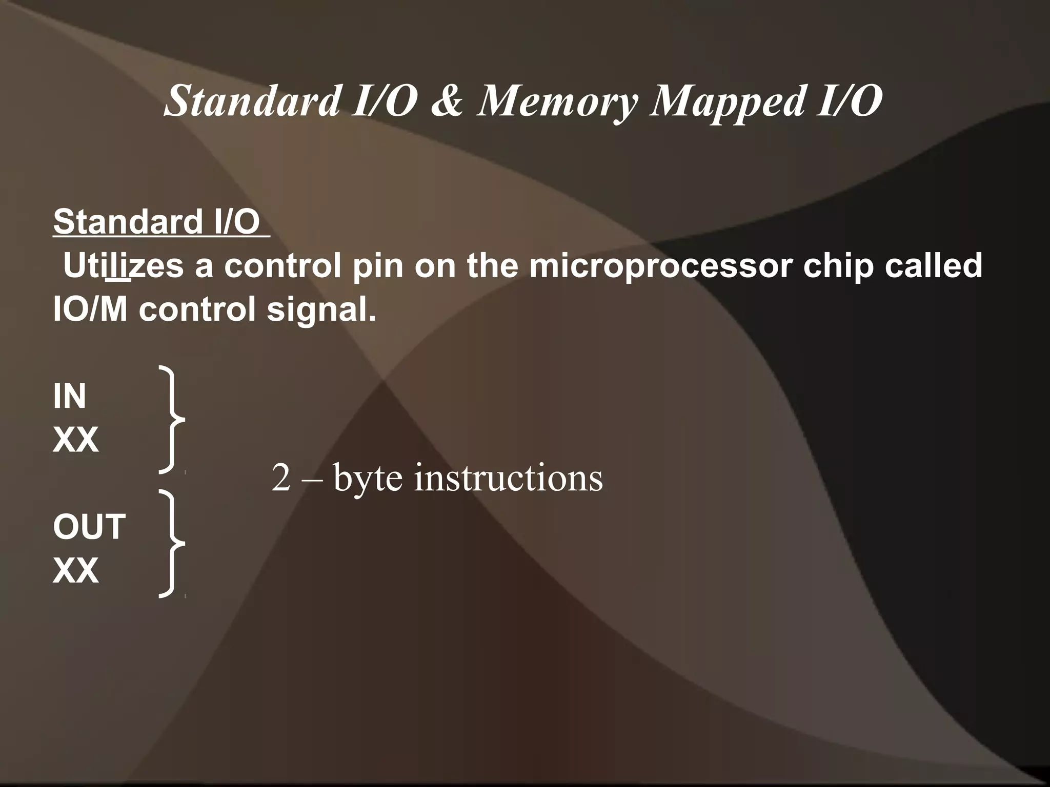
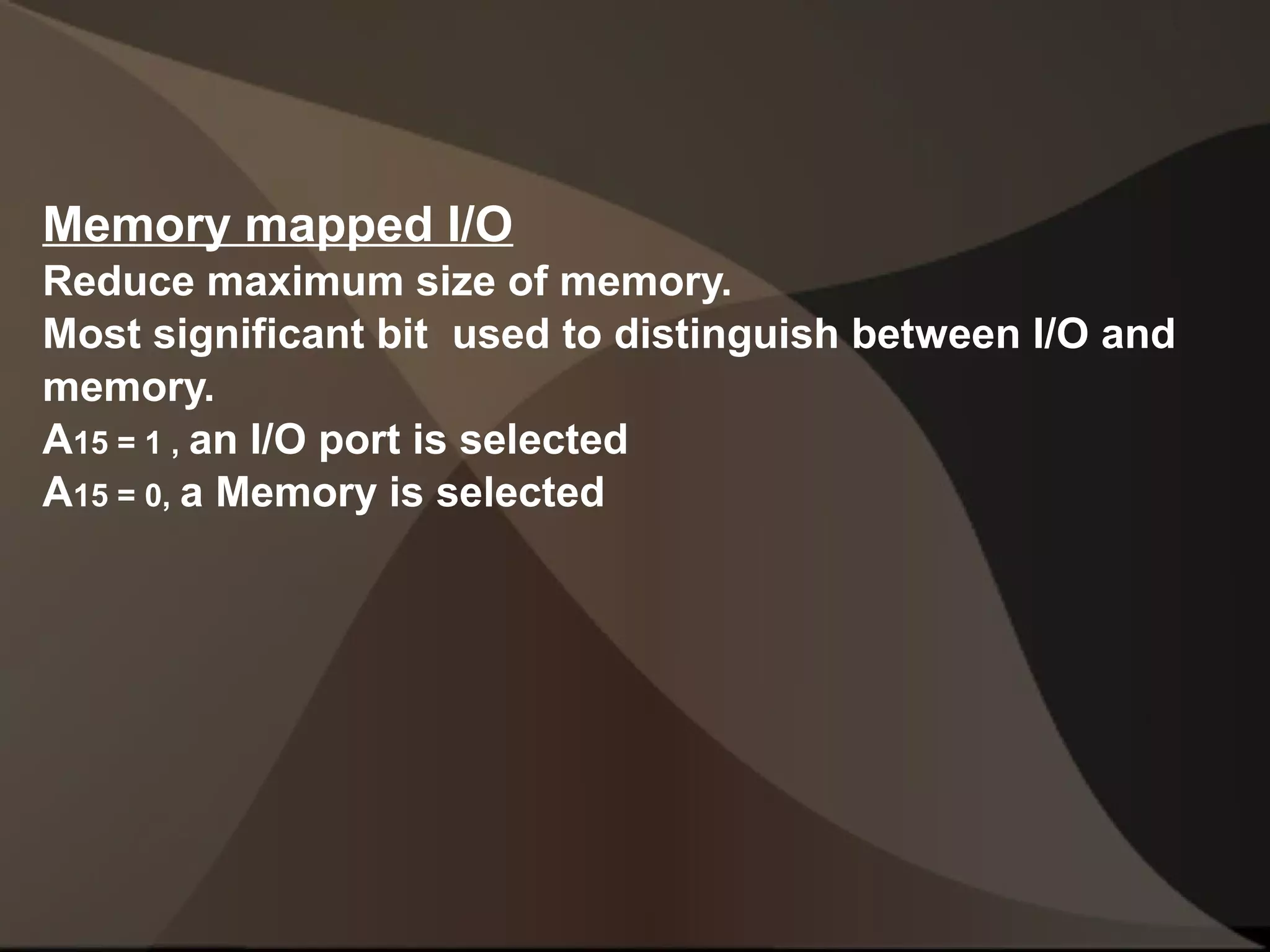
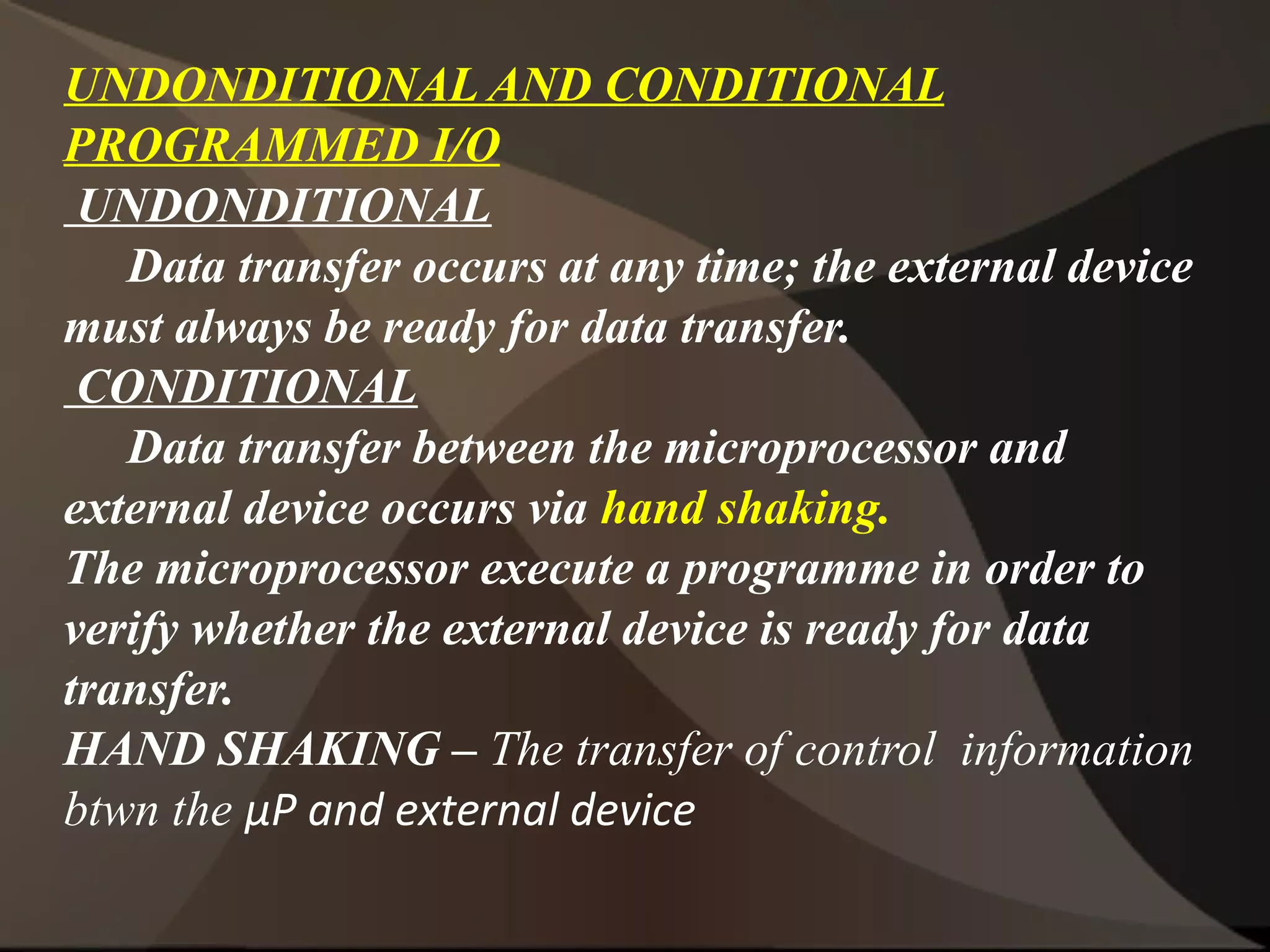
The document discusses different methods of input/output (I/O) operations in microprocessors, including programmed I/O, interrupt I/O, and direct memory access (DMA). Programmed I/O involves the microprocessor executing instructions to transfer data via I/O ports. Interrupt I/O allows external devices to trigger an interrupt service routine. DMA allows data transfers directly between memory and external devices without microprocessor involvement using a DMA controller.


